General
Power
requirements
TABLE
OF
CONTENTS
|
US,
Canadian
model
_|
Canadian
model
1
120V
AC,60Hz
AC,
60Hz
Sensual
;
AEP,
UK,
German,
PECIFICALIONS
*srsrttr
etc
te
tees
eetee
eee
een
teen
eenee
ene
aeeeneeteeeeaeeenes
Serta
are
ce
tae
te
Wo
|
1.
GENERAL
1-1.
Identifying
the
Parts
Pte
ener
n
amma
m
cence
reese
eeesnesaresareeees
4
Power
consumption
_
26W
2.
DISASSEMBLY
Dimensions
(approx)
(w/h/d)
D1.
EeGint
PARE
iiss
iaeeiiaodas
uk
aswaup
uaa
taeninnteatiban
omntaees
5
Model
for
U.K.
and
Australian
:
35
<Naechiatiisin:
Peele
ses
ise
secs
aoe
waded
See
shat
Geena
hess
5
430x
123
*300mm
(w/h/
qd)
2-3.
Capstan
Motor,
Reel
Motor
v+r+tesssseessseseeeeseteeeneeeees
6
(17x
47%
x
11%
inches)
Sat
Pent
Pinch
Rolle
sien
ne
ele
eae
6
Model
for
other
countries
:
;
:
430X123
X290mm
(w/h/d)
(17x
47%
x
11'A
inches)
3.
ADJUSTMENTS
~
including
projecting
parts
and
controls
3-1,
Mechanical
Adjustments
eee
ccc
c
cen
serncneneeeenssesevevecerees
7
Mass
(Approx.)
3.2.
Blectrical
Adjustments
Peeve
rece
rere
rere
nee
neseeeneneererseees
7
4.5kg
(9Ibs
150z)
Supplied
accessories
4.
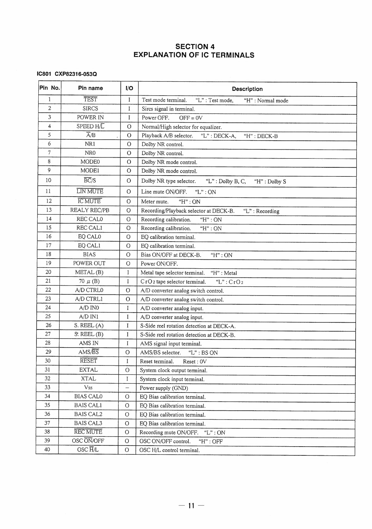
EXPLANATION
OF
IC
TERMINALS
-:-+++++-++-+-0+++
++
11
Audio
connecting
cords
(2
phono
plug-2
phone
plugs)
(2)
Optional
accessory
5.
DIAGRAMS
Remote
commander
RM-J902
5-1.
Block
Diagrams
:::++tssstesssssessseeessseneeserseeeseeereenes
13
es:
.
5-2.
Printed
Wiring
Boards
(System
Control
Section)-:--+::
17
Design
and
specifications
are
subject
to
change
without
notice.
5-3.
Schematic
Diagram
(System
Control
Section)+++++++++«
4
5-4.
Schematic
Diagram
(Audio
Section)
s++t+rrterrreeter
sees
27
5-5.
Printed
Wiring
Boards
(Audio
Section)-++++++rrrtsreres
31
5-6.
Printed
Wiring
Boards
(Dolby
(S)
Section)
:+++++++-++++-
34
5-7.
Schematic
Diagram
(Dolby
(S)
Section)
sorrrretrtereee
34
6.
EXPLODED
VIEWS
G2).
Chassis
Sections
torsion
Aeeananeessees
yenernavseneehigieteniecs
37
672:
Front
Panel
Section:
sth
ee
std
srentaiecesstascereseedstea
39
6-3.
Mechanism
Section.
|
<1.0+407serss
esse
eeanseuese
a
satanetves
40
6-4:
Mechanism
Section
2
ican
aarti
wl
asceseaiinciisanewes
4]
7.
ELECTRICAL
PARTS
LIST
«---::-scccsseceresssecsececeesenes
42
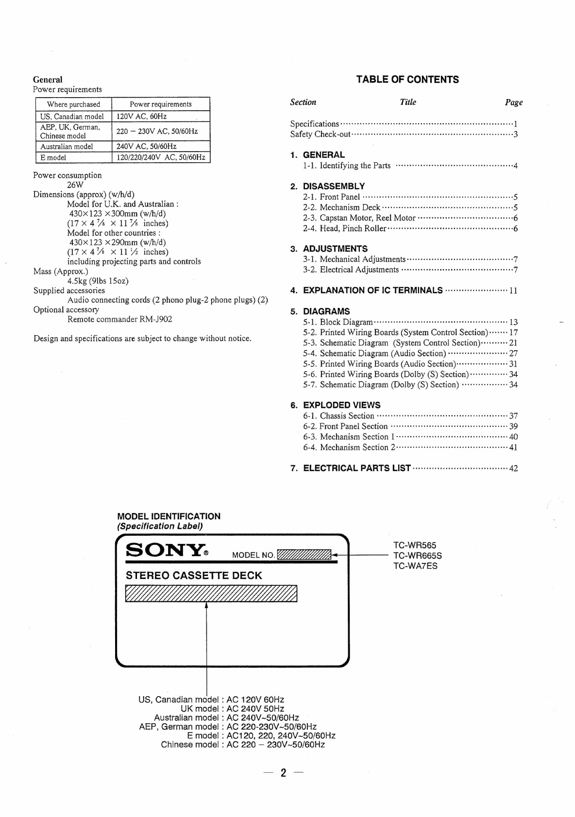
MODEL
IDENTIFICATION
(Specification
Label)
SONY
alike
8
MODELND.
YY“YYW/
TC-WR665S
TC-WA7ES
US,
Canadian
model
UK
model
Australian
model
AEP,
German
model
E
model
Chinese
model
STEREO
CASSETTE
DECK
WML
:
AC
120V
60Hz
:
AC
240V
50Hz
:
AC
240V~50/60Hz
:
AC
220-230V~50/60Hz
:AC120,
220,
240V~50/60Hz
:
AC
220
—
230V~50/60Hz
—)?—


 User manual")