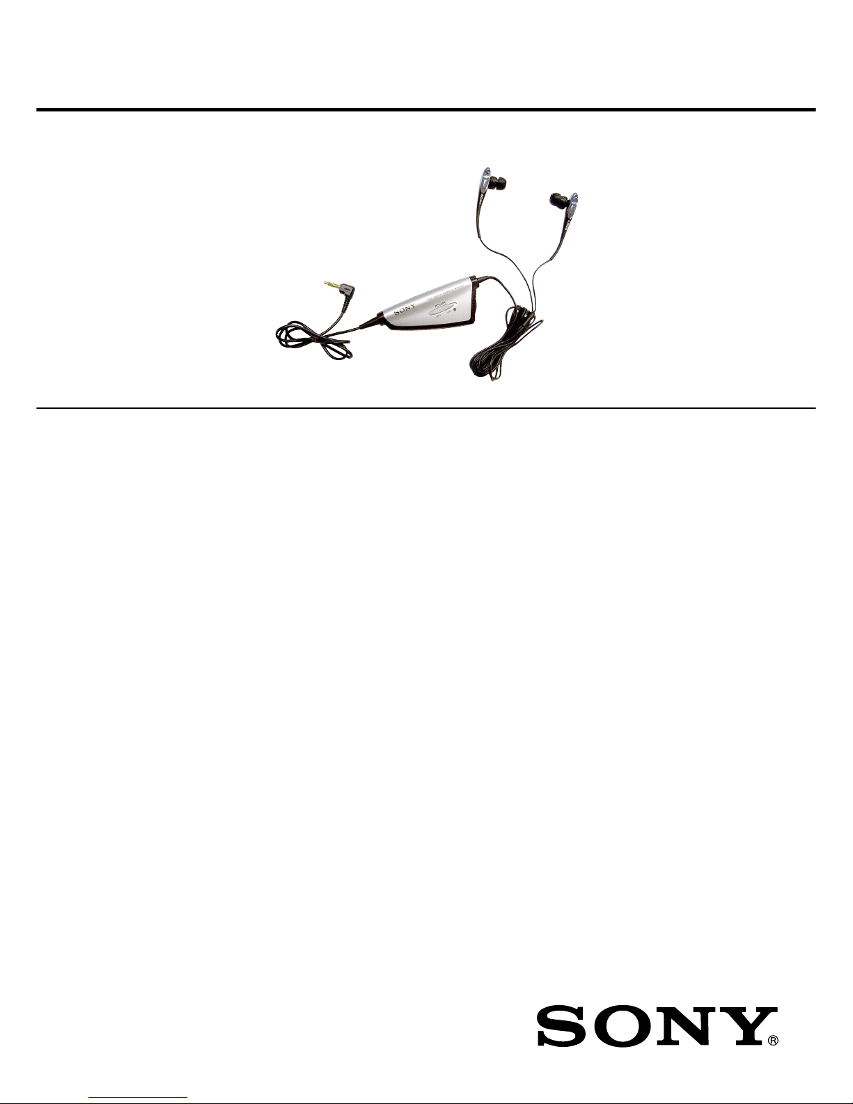
MDR-NC11
88
SECTION 5
ELECTRICAL PARTS LIST
SECTION 4
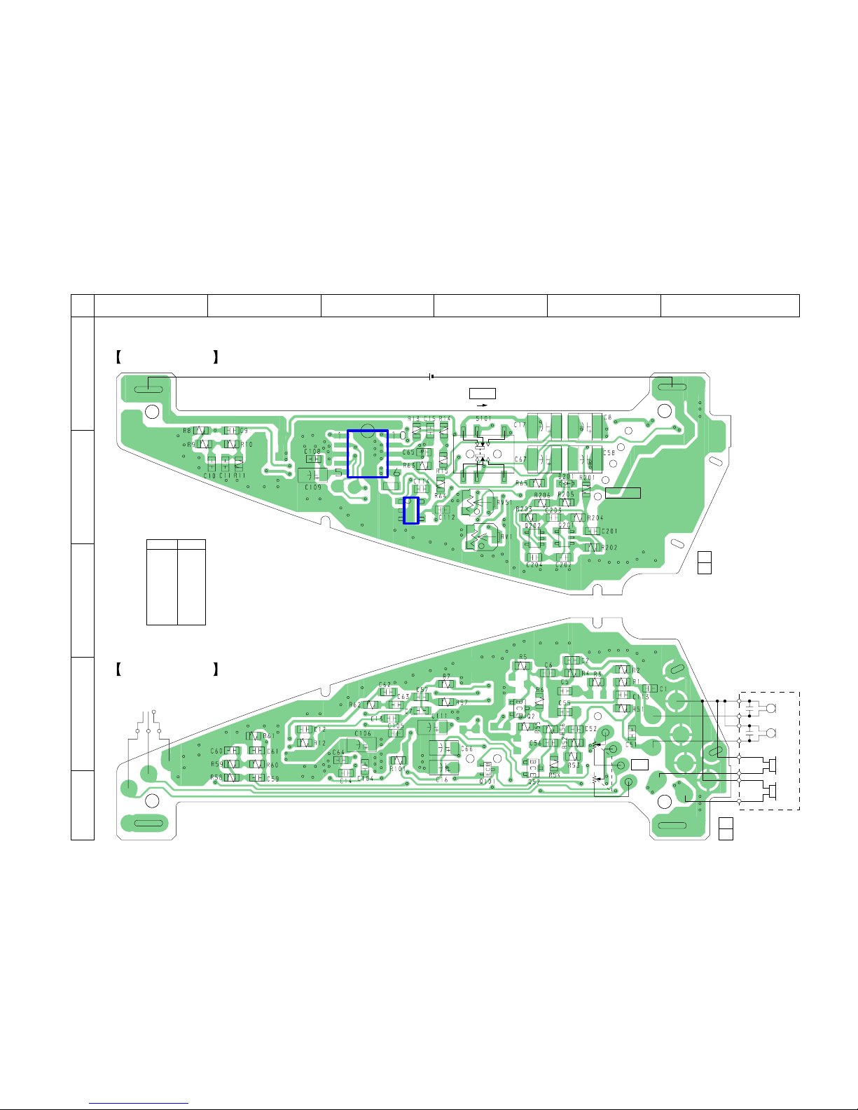
EXPLODED VIEW MAIN
Ref. No. Part No. Description Remark Ref. No. Part No. Description Remark
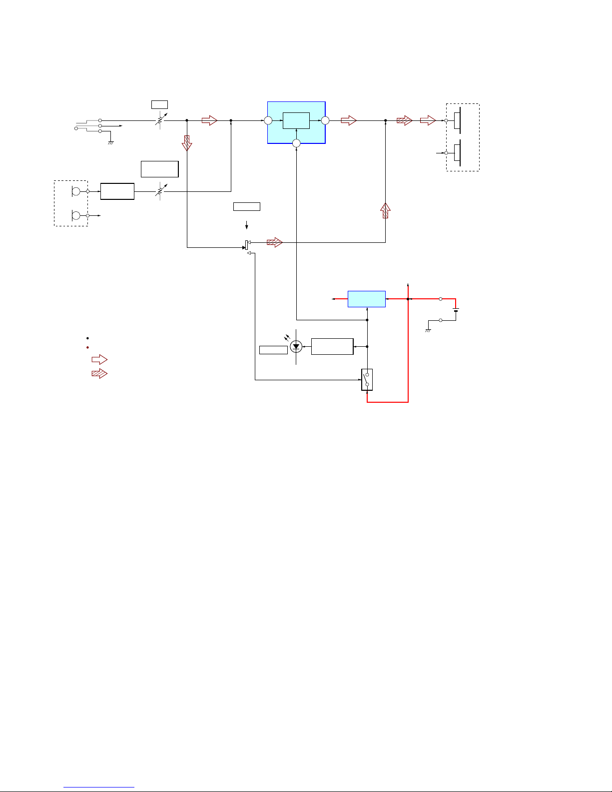
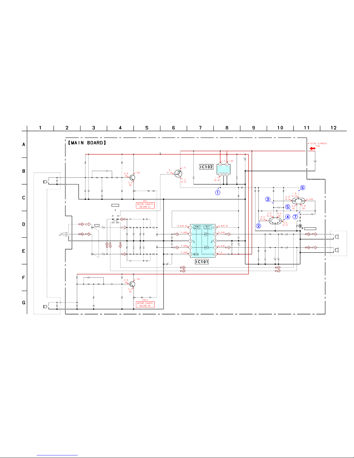
*A-3178-431-A MAIN BOARD, COMPLETE
*********************
< CAPACITOR >
C1 1-107-826-11 CERAMIC CHIP 0.1uF 10% 16V
C2 1-165-176-11 CERAMIC CHIP 0.047uF 10% 16V
C5 1-125-837-11 CERAMIC CHIP 1uF 10% 6.3V
C6 1-125-837-11 CERAMIC CHIP 1uF 10% 6.3V
C7 1-125-837-11 CERAMIC CHIP 1uF 10% 6.3V
C8 1-128-964-11 TANTALUM CHIP 100uF 20% 6.3V
C9 1-127-715-11 CERAMIC CHIP 0.22uF 10% 16V
C10 1-127-715-11 CERAMIC CHIP 0.22uF 10% 16V
C11 1-125-891-11 CERAMIC CHIP 0.47uF 10% 10V
C12 1-162-966-11 CERAMIC CHIP 0.0022uF 10% 50V
C13 1-127-715-11 CERAMIC CHIP 0.22uF 10% 16V
C14 1-162-966-11 CERAMIC CHIP 0.0022uF 10% 50V
C15 1-107-826-11 CERAMIC CHIP 0.1uF 10% 16V
C16 1-104-851-11 TANTALUM CHIP 10uF 20% 10V
C17 1-137-859-11 TANTALUM CHIP 220uF 20% 4V
C51 1-107-826-11 CERAMIC CHIP 0.1uF 10% 16V
C52 1-165-176-11 CERAMIC CHIP 0.047uF 10% 16V
C55 1-125-837-11 CERAMIC CHIP 1uF 10% 6.3V
C56 1-125-837-11 CERAMIC CHIP 1uF 10% 6.3V
C57 1-125-837-11 CERAMIC CHIP 1uF 10% 6.3V
C58 1-128-964-11 TANTALUM CHIP 100uF 20% 6.3V
C59 1-127-715-11 CERAMIC CHIP 0.22uF 10% 16V
C60 1-127-715-11 CERAMIC CHIP 0.22uF 10% 16V
C61 1-125-891-11 CERAMIC CHIP 0.47uF 10% 10V
C62 1-162-966-11 CERAMIC CHIP 0.0022uF 10% 50V
C63 1-127-715-11 CERAMIC CHIP 0.22uF 10% 16V
C64 1-162-966-11 CERAMIC CHIP 0.0022uF 10% 50V
C65 1-107-826-11 CERAMIC CHIP 0.1uF 10% 16V
C66 1-104-851-11 TANTALUM CHIP 10uF 20% 10V
C67 1-137-859-11 TANTALUM CHIP 220uF 20% 4V
C104 1-162-970-11 CERAMIC CHIP 0.01uF 10% 25V
C105 1-107-826-11 CERAMIC CHIP 0.1uF 10% 16V
C106 1-104-851-11 TANTALUM CHIP 10uF 20% 10V
C108 1-162-970-11 CERAMIC CHIP 0.01uF 10% 25V
C109 1-104-851-11 TANTALUM CHIP 10uF 20% 10V
C111 1-104-851-11 TANTALUM CHIP 10uF 20% 10V
C112 1-107-826-11 CERAMIC CHIP 0.1uF 10% 16V
C113 1-162-970-11 CERAMIC CHIP 0.01uF 10% 25V
C114 1-162-970-11 CERAMIC CHIP 0.01uF 10% 25V
C201 1-125-837-11 CERAMIC CHIP 1uF 10% 6.3V
NOTE:
• Due to standardization, replacements in the
parts list may be different from the parts speci-
fied in the diagrams or the components used
on the set.
• -XX and -X mean standardized parts, so they
may have some difference from the original
one.
• RESISTORS
All resistors are in ohms.
METAL: Metal-film resistor.
METAL OXIDE: Metal oxide-film resistor.
F: nonflammable
• Items marked “*” are not stocked since they
are seldom required for routine service.
Some delay should be anticipated when order-
ing these items.
• SEMICONDUCTORS
In each case, u: µ, for example:
uA. . : µA. . uPA. . : µPA. .
uPB. . : µPB. . uPC. . : µPC. .
uPD. . : µPD. .
• CAPACITORS
uF: µF
• COILS
uH: µH
C202 1-162-966-11 CERAMIC CHIP 0.0022uF 10% 50V
C203 1-162-966-11 CERAMIC CHIP 0.0022uF 10% 50V
C204 1-107-826-11 CERAMIC CHIP 0.1uF 10% 16V
< LED >
D201 8-719-077-09 LED CL-196HR-CD-T (POWER ON)
< IC >
IC101 8-759-835-58 IC LA4537M-TE-L
IC102 8-759-348-89 IC TK70203M
< RESISTOR >
JC101 1-216-864-11 METAL CHIP 0 5% 1/16W
< TRANSISTOR >
Q2 8-729-602-21 TRANSISTOR 2SC4154-F
Q52 8-729-602-21 TRANSISTOR 2SC4154-F
Q101 8-729-924-28 TRANSISTOR DTA123YU
Q201 8-729-050-11 TRANSISTOR UMW1NTR
Q202 8-729-055-39 TRANSISTOR UMA4N-TR
< RESISTOR >
R1 1-216-826-11 METAL CHIP 2.7K 5% 1/16W
R2 1-218-863-11 METAL CHIP 4.7K 0.5% 1/10W
R3 1-218-863-11 METAL CHIP 4.7K 0.5% 1/10W
R4 1-218-847-11 METAL CHIP 1K 0.5% 1/10W
R5 1-216-853-11 METAL CHIP 470K 5% 1/16W
R6 1-216-841-11 METAL CHIP 47K 5% 1/16W
R7 1-216-825-11 METAL CHIP 2.2K 5% 1/16W
R8 1-216-800-11 RES-CHIP 18 5% 1/10W
R9 1-218-867-11 RES-CHIP 6.8K 5% 1/10W
R10 1-216-825-11 METAL CHIP 2.2K 5% 1/16W
R11 1-216-833-11 METAL CHIP 10K 5% 1/16W
R12 1-216-833-11 METAL CHIP 10K 5% 1/16W
R13 1-216-793-11 RES-CHIP 4.7 5% 1/10W
R14 1-216-789-11 METAL CHIP 2.2 5% 1/16W
R15 1-216-796-11 RES-CHIP 8.2 5% 1/10W
R51 1-216-826-11 METAL CHIP 2.7K 5% 1/16W
R52 1-218-863-11 METAL CHIP 4.7K 0.5% 1/10W
R53 1-218-863-11 METAL CHIP 4.7K 0.5% 1/10W
R54 1-218-847-11 METAL CHIP 1K 0.5% 1/10W
R55 1-216-853-11 METAL CHIP 470K 5% 1/16W
1
2
P1
#1
#1
4
7
7
6
9
13
12 11
3
10
HP1
• Items marked “*” are not stocked since they
are seldom required for routine service. Some
delay should be anticipated when ordering
these items.
• The mechanical parts with no reference num-
ber in the exploded views are not supplied.
• Accessories are given in the last of the elec-
trical parts list.
NOTE:
• -XX and -X mean standardized parts, so they
may have some difference from the original
one.
• Color Indication of Appearance Parts
Example:
KNOB, BALANCE (WHITE) . . . (RED)
↑↑
Parts Color Cabinet's Color
Ref. No. Part No. Description Remark Ref. No. Part No. Description Remark
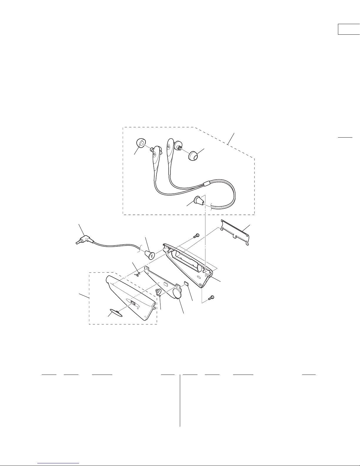
1 3-235-824-01 KNOB, POWER
2 X-3381-832-1 CASE (UPPER) SUB ASSY
3 3-330-637-01 CUSHION (T)
4 3-236-543-01 BUSHING (LOWER), BATTERY CASE
6 3-235-828-01 BUSHING (UPPER), BATTERY CASE
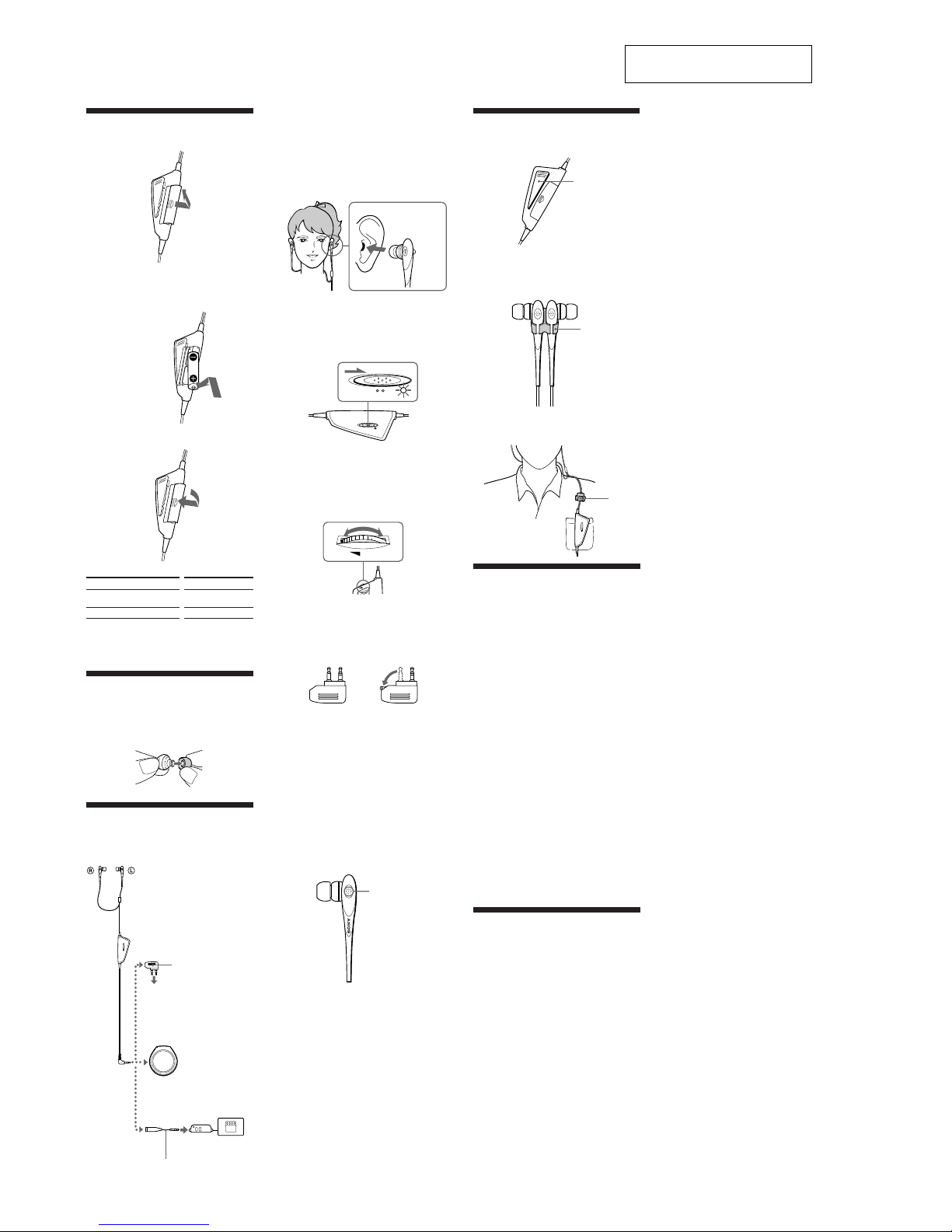
7 4-220-438-01 PIECE (M), EAR (CLEAR BLUE BLACK)
7 4-220-438-21 PIECE (M), EAR (CLEAR BLACK)
9 3-235-820-01 LID, BATTERY CASE
10 X-3382-038-1 CASE (LOWER) SUB ASSY
*11 A-3178-431-A MAIN BOARD, COMPLETE
12 3-235-827-01 TERMINAL (-), BATTERY
13 3-235-826-01 TERMINAL (+), BATTERY
HP1 A-3174-443-A HEADPHONE ASSY
P1 1-823-514-11 CORD (WITH PLUG)
#1 7-685-102-19 SCREW, +P 2X4 TYPE2 NON-SLIT
The components identified by
mark 0or dotted line with mark
0are critical for safety.
Replace only with part number
specified.
When indicating parts by reference
number, please include the board.
Ver 1.1

 User manual")


 User manual")