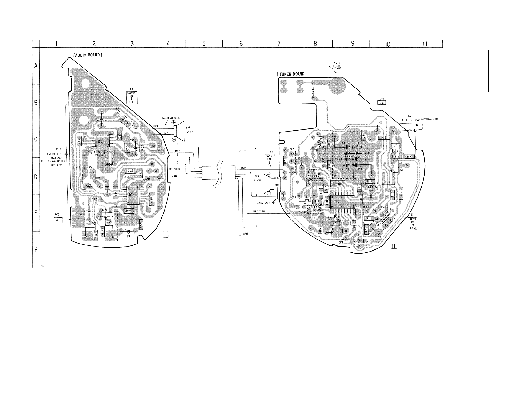
*A-3670-048-A AUDIO BOARD, COMPLETE
**********************
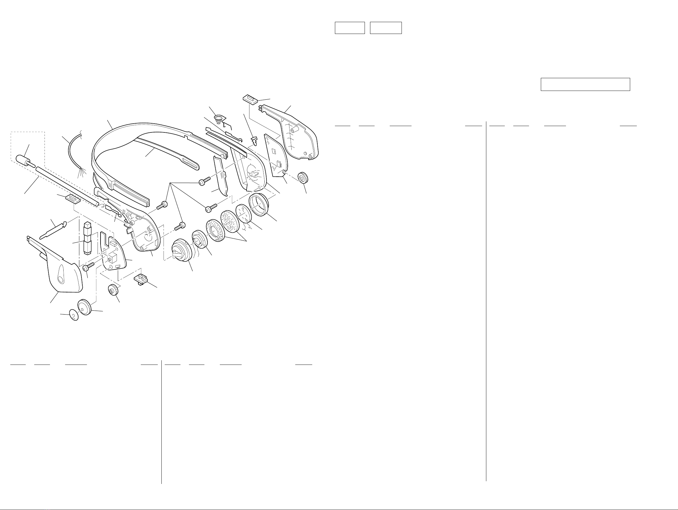
3-902-546-01 TERMINAL (PLUS), BATTERY
< CAPACITOR >
C19 1-104-396-11 ELECT 10uF 20.00% 16V
C20 1-162-637-11 CERAMIC CHIP 0.47uF 16V
C21 1-163-081-00 CERAMIC CHIP 0.22uF 25V
C22 1-162-637-11 CERAMIC CHIP 0.47uF 16V
C23 1-163-275-11 CERAMIC CHIP 0.001uF 5.00% 50V
C24 1-163-022-00 CERAMIC CHIP 0.012uF 10% 50V
C25 1-163-022-00 CERAMIC CHIP 0.012uF 10% 50V
C26 1-162-638-11 CERAMIC CHIP 1uF 16V
C27 1-162-638-11 CERAMIC CHIP 1uF 16V
C28 1-163-117-00 CERAMIC CHIP 100PF 5% 50V
C29 1-163-117-00 CERAMIC CHIP 100PF 5% 50V
C30 1-124-229-00 ELECT 33uF 20% 10V
C31 1-163-077-00 CERAMIC CHIP 0.1uF 10% 25V
C32 1-124-635-00 ELECT 220uF 20.00% 6.3V
C33 1-163-077-00 CERAMIC CHIP 0.1uF 10% 25V
C34 1-163-077-00 CERAMIC CHIP 0.1uF 10% 25V
C35 1-124-635-00 ELECT 220uF 20.00% 6.3V
C36 1-124-635-00 ELECT 220uF 20.00% 6.3V
C37 1-163-031-11 CERAMIC CHIP 0.01uF 50V
< DIODE >
D1 8-719-981-95 DIODE MTZJ-2.7B
< IC >
IC2 8-759-945-89 IC BA1362FST1
IC3 8-759-822-48 IC LA4537M
< RESISTOR >
R22 1-216-049-11 RES-CHIP 1K 5% 1/10W
R23 1-216-069-00 METAL CHIP 6.8K 5% 1/10W
R24 1-216-296-91 SHORT 0
R25 1-216-296-91 SHORT 0
R26 1-216-084-00 METAL CHIP 30K 5% 1/10W
R27 1-216-084-00 METAL CHIP 30K 5% 1/10W
< VARIABLE RESISTOR >
RV1 1-228-994-00 RES, ADJ, METAL10K
RV2 1-241-130-00 RES, VAR, CARBON 20K/20K (VOL)
< SWITCH >
S3 1-553-510-11 SWITCH, SLIDE (POWER)
************************************************************
*A-3683-222-A TUNER BOARD, COMPLETE
**********************
3-831-441-99 CUSHION
3-902-555-01 SHEET (FERRITE-ROD ANTENNA)
< FILTER >
BPF1 1-236-839-11 FILTER, BAND PASS
< CAPACITOR >
C1 1-163-021-91 CERAMIC CHIP 0.01uF 10.00% 50V
C2 1-126-514-11 ELECT 22uF 20.00% 6.3V
C3 1-126-117-11 ELECT 330uF 20.00% 2V
C4 1-126-117-11 ELECT 330uF 20.00% 2V
C5 1-163-077-00 CERAMIC CHIP 0.1uF 10% 25V
C6 1-163-129-00 CERAMIC CHIP 330PF 5% 50V
C7 1-162-638-11 CERAMIC CHIP 1uF 16V
C8 1-163-222-11 CERAMIC CHIP 5PF 0.25PF 50V
C9 1-162-638-11 CERAMIC CHIP 1uF 16V
C10 1-163-100-00 CERAMIC CHIP 20PF 5% 50V
C11 1-163-077-00 CERAMIC CHIP 0.1uF 10% 25V
C12 1-163-021-91 CERAMIC CHIP 0.01uF 10.00% 50V
C13 1-163-101-11 CERAMIC CHIP 22PF 5.00% 50V
C14 1-163-093-00 CERAMIC CHIP 10PF 5% 50V
C15 1-126-154-11 ELECT 47uF 20% 6.3V
C16 1-163-033-91 CERAMIC CHIP 0.022uF 50V
C17 1-163-129-00 CERAMIC CHIP 330PF 5% 50V
C18 1-163-014-00 CERAMIC CHIP 0.0027uF 10.00% 50V
< FILTER >
CF1 1-567-097-61 FILTER, CERAMIC
CF2 1-578-677-11 FILTER, CRYSTAL
< VARIABLE CAPACITOR >
CV1 1-151-620-11 CAP, VARIABLE (TUNE)
< TRIMMER >
CT1 1-151-620-11 CAP, VARIABLE
< IC >
IC1 8-759-230-65 IC TA7792F
< COIL >
L1 1-414-142-61 INDUCTOR 1uH
L2 1-402-505-11 ANTENNA, FERRITE-ROD (MW)
L3 1-428-123-11 COIL, AIR-CORE
L4 1-428-122-11 COIL, AIR-CORE
L5 1-406-390-21 COIL (OSC)
AUDIO TUNER
Ref. No. Part No. Description Remarks Ref. No. Part No. Description Remarks
SECTION 6
ELECTRICAL PARTS LIST
NOTE:
• Due to standardization, replacements in the
parts list may be different from the parts
specifiedin the diagrams or the components
used on the set.
• -XX, -X mean standardized parts, so they
may have some difference from the original
one.
• Items marked “*” are not stocked since they
are seldom required for routine service.
Some delay should be anticipated when
ordering these items.
• CAPACITORS:
uF: µF
• RESISTORS
All resistors are in ohms.
METAL: metal-film resistor
METAL OXIDE: Metal Oxide-film resistor
F: nonflammable
• COILS
uH: µH
• SEMICONDUCTORS
In each case, u: µ, for example:
uA...: µA... , uPA... , µPA... ,
uPB... , µPB... , uPC... , µPC... ,
uPD..., µPD...
When indicating parts by reference number,
please include the board name.
Ref. No. Part No. Description Remarks Ref. No. Part No. Description Remarks
*1 A-3683-222-A TUNER BOARD, COMPLETE
2 X-3379-444-1 CABINET FRONT (R) ASSY
3 3-902-544-01 GEAR(TUNING)
4 3-902-551-01 SCALE(FM/AM), DIAL
5 3-309-597-31 SCREW(1.4), TAPPING,PRECISION
6 3-902-555-01 SHEET(FERRITE-ROD ANTENNA)
*8 3-902-552-01 PLATE, CLICK
9 3-902-546-01 TERMINAL (PLUS), BATTERY
10 X-3379-445-1 CABINET FRONT (L) ASSY
11 3-902-542-01 KNOB
12 3-902-547-01 SPRING, BATTERY COIL
13 3-318-203-51 SCREW (B1.7X12), TAPPING
14 3-363-940-01 PAD, EAR
15 3-902-539-01 LID, BATTERY CASE
*16 A-3670-048-A AUDIO BOARD, COMPLETE
17 3-902-549-01 CAP, ANTENNA
18 1-575-829-11 CORD, CONNECTION
19 3-902-542-11 KNOB
20 3-902-556-11 BELT, MAIN
21 3-902-537-11 BELT (SUB)
22 3-902-541-01 KNOB (VOLUME)
23 3-902-560-01 CABINET (REAR) (L)
24 3-902-538-01 HOLDER
25 3-902-538-01 HOLDER
26 3-902-543-01 KNOB (SENS)
27 3-902-540-01 KNOB (TUNING)
28 3-902-558-21 CABINET (REAR) (R)
L2 1-402-505-11 ANTENNA, FERRITE-ROD (MW)
SP1 1-505-114-11 DRIVER (HEADPHONE)
SP2 1-505-114-11 DRIVER (HEADPHONE)
ANT1 X-3379-374-1 ANTENNA ASSY
SECTION 5
EXPLODED VIEWS
NOTE:
• -XX, -X mean standardized parts, so they may
have some differences from the original one.
• Items marked “*” are not stocked since they
are seldom required for routine service. Some
delayshould be anticipated whenorderingthese
items.
• Themechanical parts withno reference number
in the exploded views are not supplied.
• Hardware (# mark) list and accessories and
packing materials are given in the last of this
parts list.
— 11 — — 12 —
18
17
6
L2
13
8
1SP2
14
SP1
3
4
2
5
15 16
10
11
9
12
8
ANT 1
20
21
19
27
26
28
25
24
22
23