— 12 —
Ref. No. Part No. Description Remarks Ref. No. Part No. Description Remarks
SECTION 6
ELECTRICAL PARTS LIST
NOTE:
• Due to standardization, replacements in the
parts list may be different from the parts
specifiedinthe diagramsor the components
used on the set.
• -XX, -X mean standardized parts, so they
may have some difference from the original
one.
• Items marked “*” are not stocked since they
are seldom required for routine service.
Some delay should be anticipated when
ordering these items.
• CAPACITORS:
uF: µF
• RESISTORS
All resistors are in ohms.
METAL: metal-film resistor
METAL OXIDE: Metal Oxide-film resistor
F: nonflammable
• COILS
uH: µH
• SEMICONDUCTORS
In each case, u: µ, for example:
uA...: µA... , uPA... , µPA... ,
uPB... , µPB... , uPC... , µPC... ,
uPD..., µPD...
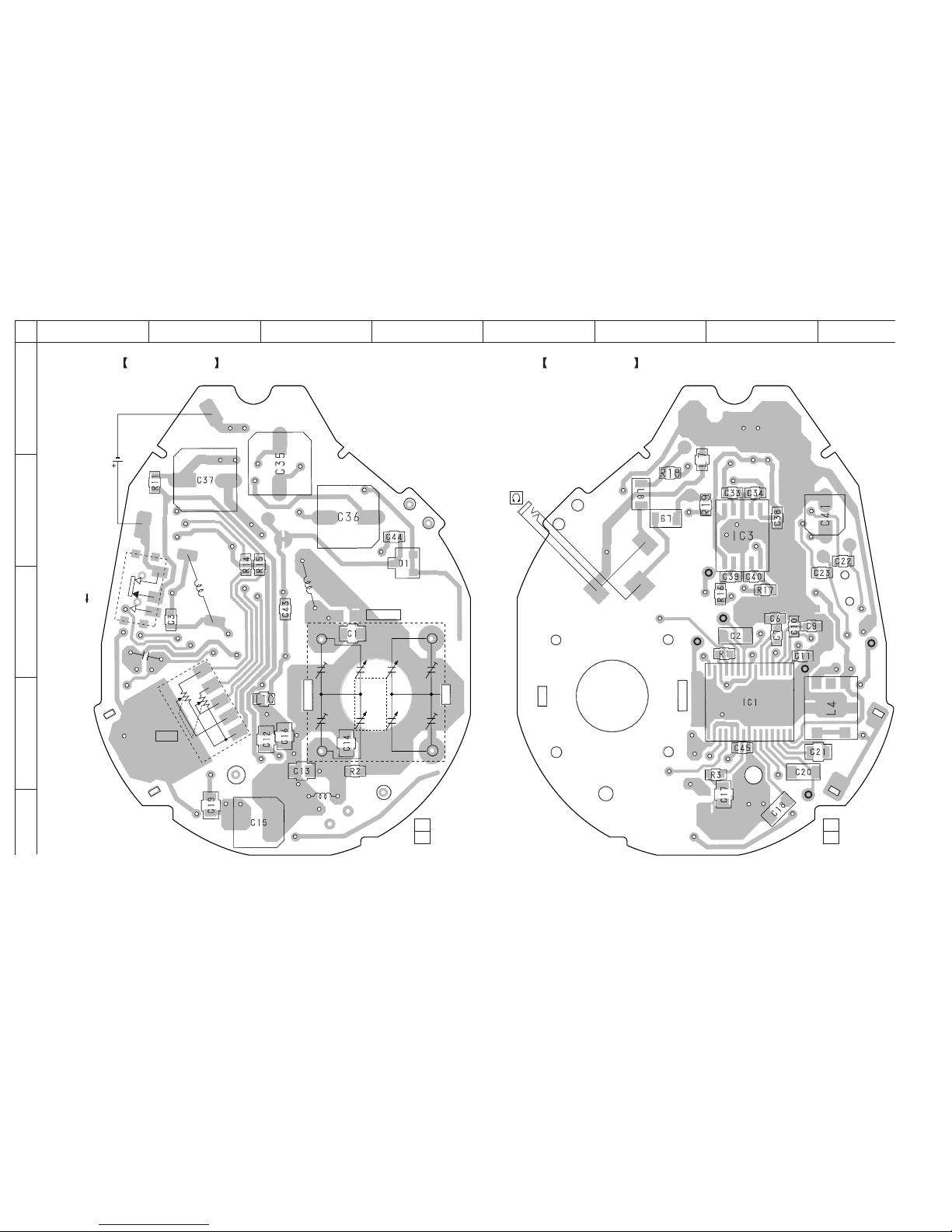
A-3663-442-A MAIN BOARD, COMPLETE
*********************
< CAPACITOR >
C1 1-163-233-11 CERAMIC CHIP 18PF 5.00% 50V
C2 1-135-181-21 TANTALUM CHIP 4.7uF 20% 6.3V
C3 1-162-927-11 CERAMIC CHIP 100PF 5% 50V
C6 1-115-156-11 CERAMIC CHIP 1uF 10V
C7 1-165-128-11 CERAMIC CHIP 0.22uF 16V
C8 1-136-683-11 FILM 0.0056uF 5.00% 100V
C9 1-165-128-11 CERAMIC CHIP 0.22uF 16V
C10 1-164-227-11 CERAMIC CHIP 0.022uF 10% 25V
C11 1-164-227-11 CERAMIC CHIP 0.022uF 10% 25V
C12 1-164-346-11 CERAMIC CHIP 1uF 16V
C13 1-163-085-00 CERAMIC CHIP 2PF 50V
C14 1-163-104-00 CERAMIC CHIP 30PF 5% 50V
C15 1-126-209-11 ELECT CHIP 100uF 20.00% 4V
C16 1-164-346-11 CERAMIC CHIP 1uF 16V
C17 1-164-346-11 CERAMIC CHIP 1uF 16V
C18 1-135-181-21 TANTALUM CHIP 4.7uF 20% 6.3V
C19 1-164-346-11 CERAMIC CHIP 1uF 16V
C20 1-135-201-11 TANTALUM CHIP 10uF 20% 4V
C21 1-164-346-11 CERAMIC CHIP 1uF 16V
C22 1-115-156-11 CERAMIC CHIP 1uF 10V
C23 1-115-156-11 CERAMIC CHIP 1uF 10V
C33 1-164-156-11 CERAMIC CHIP 0.1uF 25V
C34 1-164-156-11 CERAMIC CHIP 0.1uF 25V
C35 1-126-206-11 ELECT CHIP 100uF 20% 6.3V
C36 1-126-206-11 ELECT CHIP 100uF 20% 6.3V
C37 1-126-246-11 ELECT CHIP 220uF 20% 4V
C38 1-164-156-11 CERAMIC CHIP 0.1uF 25V
C39 1-162-927-11 CERAMIC CHIP 100PF 5% 50V
C40 1-162-927-11 CERAMIC CHIP 100PF 5% 50V
C41 1-124-778-00 ELECT CHIP 22uF 20% 6.3V
C43 1-164-357-11 CERAMIC CHIP 1000PF 5.00% 50V
C44 1-162-927-11 CERAMIC CHIP 100PF 5% 50V
C45 1-164-156-11 CERAMIC CHIP 0.1uF 25V
< VARIABLE CAPACITOR >
CV1 1-141-537-11 CAP, VAR 20PF (Tuning)
< TRIMMER >
CT1 1-141-537-11 CAP, VAR 20PF
< DIODE >
D1 8-719-800-76 DIODE 1SS226
< IC >
IC1 8-752-061-76 IC CXA1129N-T4
IC3 8-759-802-80 IC LA4535M
< JACK >
J1 1-764-624-11 JACK (HEADPHONES)
< COIL >
L1 1-411-769-11 COIL, AIR-CORE
L4 1-409-971-11 COIL (VCO)
L6 1-409-990-11 COIL, AIR-CORE
L7 1-412-987-31 INDUCTOR 4.7uH
L8 1-412-947-11 INDUCTOR 4.7uH
L9 1-412-947-11 INDUCTOR 4.7uH
L10 1-412-987-31 INDUCTOR 4.7uH
< RESISTOR >
R1 1-216-813-11 METAL CHIP 220 5% 1/16W
R2 1-216-821-11 METAL CHIP 1K 5% 1/16W
R3 1-216-795-11 RES-CHIP 6.8 5% 1/16W
R11 1-216-789-11 METAL CHIP 2.2 5% 1/16W
R14 1-216-821-11 METAL CHIP 1K 5% 1/16W
R15 1-216-821-11 METAL CHIP 1K 5% 1/16W
R16 1-216-821-11 METAL CHIP 1K 5% 1/16W
R17 1-216-821-11 METAL CHIP 1K 5% 1/16W
R18 1-216-801-11 METAL CHIP 22 5% 1/16W
R19 1-216-801-11 METAL CHIP 22 5% 1/16W
< VARIABLE RESISTOR >
RV1 1-225-467-11 RES, VAR, CARBON 30K/30K (VOL)
< SWITCH >
S1 1-572-922-11 SWITCH, SLIDE (POWER)
****************************************************************
ACCESSORIES & PACKING MATERIALS
********************************
3-042-459-01 CASE, CARRYING
3-042-460-01 HOLDER, KEY
3-042-654-11 MANUAL, INSTRUCTION
(ENGLISH,SPANISH,KOREAN,CHINESE)
8-953-301-94 RECEIVER,EAR MDR-E805LP/K4 SET
MAIN
SRF-QT1
Sony Corporation
Personal Audio Division Company 1999L1625-1
Printed in Japan ©1999.12
Published by General Engineering Dept.
9-927-625-11