manuals.online logo
Brands
  1. Home
  2. •
  3. Brands
  4. •
  5. Sony
  6. •
  7. Receiver
  8. •
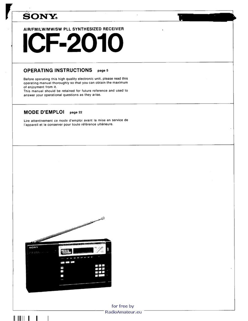
  9. Sony ICF-7600DA User manual

Sony ICF-7600DA User manual

This manual suits for next models

1

Other Sony Receiver manuals

Sony STR-DE625 - Fm Stereo/fm-am Receiver User manual

Sony

Sony STR-DE625 - Fm Stereo/fm-am Receiver User manual

Sony HCD-SHAKE10 User manual

Sony

Sony HCD-SHAKE10 User manual

Sony STR-DH810 - Audio Video Receiver User manual

Sony

Sony STR-DH810 - Audio Video Receiver User manual

Sony STR-DA3500ES User manual

Sony

Sony STR-DA3500ES User manual

Sony CX-JV1 User manual

Sony

Sony CX-JV1 User manual

Sony STR-DA3700ES Parts list manual

Sony

Sony STR-DA3700ES Parts list manual

Sony XAV-602BT User manual

Sony

Sony XAV-602BT User manual

Sony HCD-VM330AV User manual

Sony

Sony HCD-VM330AV User manual

Sony STR-DN1070 User manual

Sony

Sony STR-DN1070 User manual

Sony HCD-DX170 User manual

Sony

Sony HCD-DX170 User manual

Sony STR-DN1020 User manual

Sony

Sony STR-DN1020 User manual

Sony STR-DG810 User manual

Sony

Sony STR-DG810 User manual

Sony HCD-DZ285K User manual

Sony

Sony HCD-DZ285K User manual

Sony ICF-25 User manual

Sony

Sony ICF-25 User manual

Sony XAV-AX200 User manual

Sony

Sony XAV-AX200 User manual

Sony HCD-TZ100 User manual

Sony

Sony HCD-TZ100 User manual

Sony STR-DG520 User manual

Sony

Sony STR-DG520 User manual

Sony STR-313L User manual

Sony

Sony STR-313L User manual

Sony HDFX200 User manual

Sony

Sony HDFX200 User manual

Sony AC-VQL1BP User manual

Sony

Sony AC-VQL1BP User manual

Sony SA-TA65A User manual

Sony

Sony SA-TA65A User manual

Sony STR-DA3300ES - Multi Channel Av Receiver User manual

Sony

Sony STR-DA3300ES - Multi Channel Av Receiver User manual

Sony HCD-RV777D User manual

Sony

Sony HCD-RV777D User manual

Sony XA-1201P User manual

Sony

Sony XA-1201P User manual

Popular Receiver manuals by other brands

Televes ZAS HD SAT user manual

Televes

Televes ZAS HD SAT user manual

Realistic DX-75 Operating and service instructions

Realistic

Realistic DX-75 Operating and service instructions

Saris 4620 Assembly instructions

Saris

Saris 4620 Assembly instructions

Mini DTR 206C PVR user manual

Mini

Mini DTR 206C PVR user manual

RF Elements TwistPort manual

RF Elements

RF Elements TwistPort manual

Denon DN-200WS user guide

Denon

Denon DN-200WS user guide

Yamaha RX-V467 owner's manual

Yamaha

Yamaha RX-V467 owner's manual

Russound SaphIR 858 instruction manual

Russound

Russound SaphIR 858 instruction manual

Quasonix RDMS Firmware update procedure

Quasonix

Quasonix RDMS Firmware update procedure

Pioneer XV-HTD1 Service manual

Pioneer

Pioneer XV-HTD1 Service manual

ATZ HDMI-V2-44HE150 manual

ATZ

ATZ HDMI-V2-44HE150 manual

Grundig STR 7122 TWIN Service manual

Grundig

Grundig STR 7122 TWIN Service manual

Creative Blaster Modem user guide

Creative

Creative Blaster Modem user guide

Panduit ATLONA AT-OME-RX11 installation guide

Panduit

Panduit ATLONA AT-OME-RX11 installation guide

VOLTCRAFT UTPS-40 operating instructions

VOLTCRAFT

VOLTCRAFT UTPS-40 operating instructions

JVC KW-ADV794 instructions

JVC

JVC KW-ADV794 instructions

Litelink VT-1001 operating instructions

Litelink

Litelink VT-1001 operating instructions

Sangean WR-11 Service manual

Sangean

Sangean WR-11 Service manual

manuals.online logo
manuals.online logoBrands
  • About & Mission
  • Contact us
  • Privacy Policy
  • Terms and Conditions

Copyright 2025 Manuals.Online. All Rights Reserved.

Circuit
system
Frequency
range
Antennas
Speaker
Power
output
Outputs
Power
requirements
Battery
life
mm
MICROFILM
AEP
Model
UK
Model
E
Model
AUS
Model
ICF-7600DA:
US
Model
Canadian
Model
ICF-7700:
SPECIFICATIONS
FM:
Superheterodyne
Dimensions
Approx.
191.5
x
117
x
31.5
mm
(w/h/d)
LW/MW/SW:
Dual
conversion
superheterodyne
(7°
x
4°
x
1%
inches)
FM:
US,
Canadian
model:
76.0—108.0
MHz
including
projecting
parts
and
controls
Weight
607
g
(1
Ib
5%
oz)
AEP,
UK,
E,
AUS
model:
87.5—108.0
MHz
MW:
530-
1,700
kHz
including
batteries
Supplied
accessories
Earphone
(1)
LW:
150-285
kHz
aid
ea
SW
(1-12
SW
broadcast
bands):
3,050-
26,100
kHz
jort
wave
guide
(1)
Carrying
case
(1)
FM/SW:
Telescopic
antenna
MW/LW:
Built-in
ferrite
bar
antenna
SW
compact
antenna
(1)
Approx.
7.7
cm
(3%
inches)
dia.
400
mW
(at
10%
harmonic
distortion)
Recording
output
jack
(minijack)
output
level
0.775
mV
(—60
dB)
output
impedance
1
kilohm
Earphone
jack
(minijack)
for
8
ohm
earphone
6V
DC
Four
size
AA
(R6)
batteries
OC
IN
6
V
jack
accepts:
Sony
AC-D4S
AC
power
adaptor
(optional)
for
use
on
120
V
AC,
60
Hz
Sony
DCC-127A
or
DCC-240
car
battery
cord
(optional)
for
use
with
12
V
or
24
V
car
battery,
respectively
Sony
EBP-6
battery
case
(optional)
for
use
with
four
size
C
(R14)
batteries.
Approx.
19
hours
of
listening
for
four
hours
a
day
at
a
normal
volume,
using
Sony
batteries
SUM-3
(NS)
FM/LW/MW/SW
PLL
SYNTHESIZED
RECEIVER
SONY.
-
ICF-7600DA/7700
|
TABLE
OF
CONTENTS
Title
Description
Page
Specifications...
..................0.
1
Peatures
i
6
eis
hed
eRe
ae
ack
i
ete
2
Flexible
Circuit
Board
Repairing
........
2
Main
Board
Removal................
2
Replacing
Chip
Components...........
3
Section].
Outline......................0..
4
1-1.
Location
and
Function
of
Controls.......
4
1-2.
Outline
of
the
C-MOS
Digital-Tuning
System
IC201,
uwPD1715G
............
5
1-2-1.
Outline
of
the
Station-Selection.........
5
1-2-2.
Description
on
the
Terminals...........
5
1-2-3.
On
the
Key
Matrix..................
9
1-2-4.
Description
on
Displaying
Function
......
13
1-2-5.
Imitial-State
Setting.
..........2.....
14
1-2-6.
Muting-Output
Timings
..............
14
1-3.
Outline
of
Terminals
of
the
LCD
Dot-Matrix
Segment
Driver
IC202,
MSM5259GS......
16
1-4.
On
the
new
LCD
panel,
LCD1..........
18
Section
2.
Electrical
Adjustments...............
19
Section
3.
Diagrams....................000.
25
3-1.
Semiconductors
Lead
Layouts..........
25
3-2.
Mounting
Diagram(1)
...............
26
3-3.
Schematic
Diagram(1)...............
31
3-4.
Mounting
Diagram
(1)
...............
35
3-5.
Schematic
Diagram
(2)...............
39
3-6.
Mounting
Diagram
(2)...............
44
Section
4.
Exploded
Views
and
Parts
List..........
49
Section
5.
Electrical
Parts
List.................
$1
Troubleshooting
Guide...............
56
NOTE:
Removal
and
Block
Diagram
Sections
have
been
omitted.
FEATURES
¢
An
FM/LW/MW/SW
1-12,
15
bands
portable
radio
with
world-wide
band
coverage.
¢
A
quartz-controlled
PLL
(Phase
Locked
Loop)
synthesizer
system
using
a
microcomputer
for
easy
pinpoint
tuning.
The
tuned
frequency
is
also‘digitally
displayed.
¢
Up
to
15
stations
can
be
preset
for
button-touch
tuning.
°
An
easy
searching
a
SW
station
with
the
SW
meter
band
select
function.
¢A
timer
standby
function
to
receive
a
desired
broadcast
at
the
desired
time.
°A
sleep
timer
turns
the
radio
off
automatically
in
65
minutes.
Flexible
Circuit
Board
Repairing
1.
Keep
the
temperature
of
the
soldering
iron
at
270°
+
10°C
during
repairing.
You
can
maintain
the
temperature
of
the
soldering
iron
around
270°C
by
using
the
ther-
mal
controller
as
illustrated
on
the
right.
2.
Do
not
touch
the
soldering
iron
more
than
4
seconds
or
3
times
on
the
same
conductor
of
the
circuit
board.
3.
Do
not
apply
force
on
the
conductor
when
soldering
or
unsoldering.
Tip
of
soldering
iron
good
wrong
———_
--
_an—0"nwm—S-
MAIN
BOARD
REMOVAL
Unsolder
the
ground-connecting
pin
at
the
main
board
as
shown
below.
main
board
ground-connecting
pin
Replacing
chip
components
All
chip
components
should
be
connected
and
disconnect-
ed,
using
a
tapered
soldering
iron
[temperature
of
the
iron
tip:
less
than
280°C
(536°F)]
,
a
pair
of
tweezers
and
braid-
ed
wire.
Precautions
for
replacement
1.
Do
not
disconnect
the
chip
component
forcefully.
Otherwise,
the
pattern
may
peel
off.
.
Never
re-use
a
disconnected
chip
component.
Dispose
of
all
old
chip
components.
.
To
protect
the
chip
component,
heating
time
for
attach-
ing
the
component
should
be
within
3
seconds.
©
Removing
chip
components
(1)
Removing
solder
at
electrode
Remove
the
solder
at
the
electrode,
using
a
thin
braided
wire.
Do
not
remove
the
solder
of
the
part
(chip
component)
attached
adjacent
to
the
electrode.
Pattern
Braided
wire
(2)
Disconnecting
chip
components
Turn
the
tweezers
with
the
soldering
iron
alternately
applied
to
both
electrodes,
and
the
chip
component
will
be
disconnected.
Take
careful
precautions
while
disconnecting,
because
if
the
chip
component
is
force-
fully
removed
the
land
may
peel
off.
lsever
re-use
a
disconnected
chip
component.
Turn
Tweezers
i
(3)
Smoothing
the
soldered
surface
After
disconnecting
the
chip
component,
remove
the
solder
by
using
a
braided
wire
to
smooth
the
land
surface.
O°
Connecting
chip
components
The
value
of
chip
components
is
not
displayed
on
the
main
body.
Take
due
precautions
to
avoid
mixing
new
chip
components
with
other
ones.
(1)
Applying
solder
to
land
on
one
side
Apply
a
thin
layer
of
solder
to
the
land
on
one
side
where
the
chip
component
is
to
be
connected.
Too
much
solder
may
cause
bridging.
Small
BX
(2)
Speedy
soldering
Hold
the
chip
component
at
the
desired
position,
using
tweezers,
and
apply
the
soldering
iron
in
the
arrow-marked
direction.
To
protect
the
chip
compo-
nent,
heating
time
should
be
within
3
seconds.
Soldering
iron
cA)
Land
Printed
circuit
board
(3)
Speedy
soldering
of
electrode
on
the
other
side
Solder
the
electrode
on
the
other
side
in
the
same
way
as
in
(2)
above.
1-1.
LOCATION
AND
FUNCTION
OF
CONTROLS
Front
panel
STANDBY
(timer
standby)
button
ALARM
TIME
SET
button
CLOCK
TIME
SET
button
KEY
PROTECT
button
SECTION
1
OUTLINE
SLEEP
timer
button
MAIN
POWER
switch
ON:
To
turn
on
the
radio
or
to
set
the
timer.
OFF:
When
carrying
the
radio.
The
radio
is
kept
turned
off
even
if
the
ON/OFF
button
is
accidentally
pressed.
ON/OFF
button
Speaker
Hand
strap
TUNING
indicator
Lights
up
when
the
signal
is
received.
TUNING/TIME
ADJ
(tuning/time
adjustment)
control
TONE
control
Adjust
the
tone
quality
to
your
preference.
Normally
set
the
control
to
MUSIC.
When
the
noise
is
severe
during
SW
reception,
set
it
to
NEWS.
The
noise
May
be
reduced
to
some
extent
and
the
vocal
part
will
be
heard
more
clearly.
<=
mb
SELECT
—
(meter
band
select)
button
Band
select
buttons
(Sw,
MW/LW,
FM)
Radio
stand
Lift
up
the
stand
for
table
use.
If
the
stand
comes
off,
put
it
back
into.
Telescopic
antenna
ALARM
selector
(RADIO/BUZZER)
Recording
output
jack
@
Earphone
jack
When
the
earphone
is
plugged
in,
the
sound
from
the
speaker
does
not
come
out.
DC
IN
6
V
(extemal!
power
input)
jack
MW
CH
STEP
selector
Battery
compartment
PRESET
buttons
VOLUME
control
to
decrease
the
volume
to
increase
the
volume
tome
=
qerrieevige
MIN
MAX
ENTER
button
Display
window
The
indications
appear
as
follows.
KEY
PROTECT
indicator
Time/frequency
indicator
MAIN
POWER
indicator
PRESET
number
indicator
Band
indicator
FM,
MW/LW
band
scales
SW
meter
band
scales
CLOCK/ALARM/STANDBY/SLEEP
indicators
BUZZER
ALARM
indicator
1-2.
OUTLINE
OF
THE
C-MOS
DIGITAL-TUNING
SYSTEM
1C201,
uPD1715G-529.
1-2-1.
OUTLINE
OF
THE
STATION-SELECTION
1)
Receiving-frequency
Coverages:
The
following
table
shows
the
frequency
coverages
the
uPD1715G-529
can
receive.
CHANNEL
NUMBER
OF
NOMINAL
|
INTERMEDIATE
FREQUENCY
COVERAGE
|
SrepaRATION
|
CHANNEL
SPACING
__|
FREQUENCY
150kHz~
285kHz
|
3kHz
|
46ch
3kHz
10.71MHz
d31kHz~
1,602kHz
3kHz
359ch
3kHz
10.71MHz
030kHz~
1,700kHz
5kHz
235ch
5kHz
10.71MHz
3,050kHz~
3,565kHz
5kHz
104ch
5kHz
10.71MHz
3,700kHz~
4,215kHz
5kHz
104ch
5kHz
10.71MHz
4,650kHz
~
5,165kHz
5kHz
104ch
okHz
10.71MHz
5,800kHz
~
6,315kHz
5kHz
104ch
5kHz
10.71MHz
6,950kHz~
7,465kHz
5kHz
104ch
5kHz
10.71MHz
9,375kHz
~10,010kHz
5kHz
128ch
5kHz
10.71MHz
11,525kHz
~12,160kHz
5kHz
128ch
5kHz
10.71MHz
13,375kHz
~14,010kHz
5kHz
128ch
5okHz
10.71MHz
14,975kHz
~15,610kHz
5kHz
128ch
okHz
10.71IMHz
17,475kHz
~18,110kHz
5kHz
128ch
okHz
10.71MHz
21,325kHz
~21,960kHz
5kHz
128ch
okHz
|
10.71MHz
25,475kHz
~26,100kHz
okHz
126ch
okHz
10.71MHz
87.50MHz~108.00MHz
|
50kHz
41l1ch
ds0kHz
10.7MHz
76.00MHz
~
108.00
MHz
30kHz
|
50kHz
10.7MHz
NOTE:
LW
and
MW1
(or
MW2)
bands
are
taken
into
a
single
band
in
the
uPD1715G-529.
+
2)
Station-selecting
Functions:
a)
Manual
up/down
selection
by
using
the
rotary
encoder
tuning
dial.
b)
Random
selection
out
of
the
preset
memories
by
key-in
calling.
LW
and
MW
bands:
5
stations
SW
band:
5
stations
FM
band:
5
stations
total
15
stations
c)
Last-channel
memory
writing
and
calling:
One
channel
is
provided
for
each
receiving
band,
total
of
15
(fifteen).
1-2-2.
DESCRIPTION
ON
THE
TERMINALS
1)
Terminal
Arrangement
((8)
VDP/PG
2
(7)
Vss
2
(cap
|
(8)
cap
2
(14)
Vss
3
SYMBOL
NAMING
DESCRIPTION
1
THRU
10
LCD9
THRU
LCD1
LCD
SEGMENT
SIGNALS
Transmit
the
segment-output
signals
to
the
LCD
panel.
When
matrixes
are
configured
together
with
the
COM1
thru
COM3,
a
display
of
48
dots
can
be
made.
These
output
signals
are
output
when
the
LCDD
commands
are
made.-The
LCD-driving
voltages
are
of
3.1V
typi-
cal,
1/2
bias
and
1/3
duty
when
the
frame
frequency
is
100
Hz.
These
LCD11
through
LCD16
can
also
be
used
at
the
same
time
as
the
key
source
signals
for
the
key
matrix.
These
signal
are
output
on
time-division
bases,
and
they
are
output
as
the
key-source
signals
at
the
repetition
rate
of
6.7
msec.
Whether
the
key-source
signal
are
to
be
output
while
having
displays
on
the
panel
is
depend-
ent
upon
and
selectable
by
the
programs
used.
These
terminals
become
automatically
in
the
““L”
(low)
state,
i.e.,
non-display
mode,
at
the
power-on
reset
(VDD
changes
from
low
to
high
state)
and
at
the
stoppage
moment
of
the
clock.
The
display
mode
does
not
change
at
the
reset
moment
in
which
CE
changes
from
low
to
high
state.
:
11
THRU
13
LCD
COMMON
SIGNAL
VDP
(POWER-
OUTPUT)
CGP
(MUTE/
BUZZER)
CAPACITOR
CONNECTION
TERMINAL
FOR
DOUBLER
VARIABLE
DUTY
PORT
(POWER-
SUPPLY
CONTROL
SIGNAL)
CLOCK
GENERATOR
PORT
(MUTE/
BUZZER
SIGNAL)
INPUT
OF
POWER
SUPPLY
VOLTAGE
Transmit
common
signals
to
the
LCD
panel.
When
the
matrixes
are
configured
together
with
the
LCD1
through
LCD16,
a
display
of
48
dots
can
be
made.
Three
distinctive
signals
of
VSS3,
VSS2
and
VDD
are
output
through
these
terminals
at
the
repetition
rate
of
50
Hz.
These
terminals
become
automatically
in
the
‘““L”’(low)
state,
i.e.,
non-display
mode,
at
the
power-on
reset
(VDD
changes
from
low
to
high
state)
and
at
the
stoppage
moment
of
the
clock.
Capacitor-connection
terminals
to
make
a
proper
voltage
doubler
to
build
the
3.1V
typi-
cal
LCD-driving
voltage
VDD.
Normal
circuit
configuration
is
as
follows.
Outputs
the
variable-duty
or
the
one-bit
(PG2)
signal.
The
selection
of
either
of
them
is
programmable.
When
used
as
the
VDP,
this
terminal
transmits
the
pulse
chain
of
1.12
kHz
continuously,
and
its
duty
can
be
selected
from
the
available
64
steps.
26.7
us
867
us
2
65
=
uw
ir
893us
893us
67
67
This
port
can
be
used
as
a
D/A
converter
by
adding-an
integration
circuit
to
this
terminal.
Outputs
the
clock-generator
or
the
one-bit
(PD3)
signal.
The
selection
of
either
of
them
is
programmable.
When
used
as
the
CGP,
this
terminal
can
transmit
the
pulse
chain
of
1
kHz
of
46.6%
duty
or
3
kHz
of
60%
duty.
In
this
set,
this
port
outputs
a
signal
to
mute
noises
encoutered
in
the
unlocked
condition
of
the
PLL.
When
the
buzzer
output
is
specified
to
be
output
in
the
alarm
operation,
this
port
outputs
the
buzzer
signal
of
1
kHz.
Receives
the
power-supply
voltage
for
this
device.
In
operation,
a
voltage
of
2.2
to
3.5
VDC
is
applied
to
this
terminal.
The
input
voltage
can
be
lowered
down
to
2.0
VDC
when
any
of
the
interna]
data
in
the
RAM,
i.e.,
when
the
CKSTP
command
is
under
execution,
is
to
be
holded.
The
power-on
reset
circuit
of
device
starts
to
operate
at
the
instance
this
terminal
receives
a
voltage
of
0
(zero)
to
2.0
VDC,
and
the
program
starts
from
the
location
0
(zero).
Note:
This
pin
and
pin
46
are
connected
internally.
So,
it
is
not
necessary
to
apply
the
power-supply
voltage
to
both
of
them.
The
ceramic-packaged
device,
however,
has
a
not-to-be
connected
pin
46,
i.e.,
N.C.
terminal.
CONTROL-
SIGNAL
INPUT
FOR
DIVIDER
Determines
the
dividing
ratio
of
the
fixed-division
prescaler.
A
1/4
dividing
ratio
is
made
when
this
terminal
is
held
at
‘““H”
(high),
and
a
1/2
divider
is
made
when
held
at
“‘L”’
(low).
This
port
is
used
only
when
the
VCOH
terminal
(FM
in
this
set)
i.e.,
pin
22
is
used.
This
set
uses
this
port
asa
1/4
divider.
FM
OSC
SIGNAL
INPUT
Receives
frequencies
from
10
MHz
to
130
MHz
or
from
10
MHz
to
100
MHz
both
of
a
level
of
0.2
Vp-p
minimum
from
the
local-oscillator
output,
i.e.,
the
VCO
output.
This
input
signal
is
connected
internally
in
this
device
through
the
1/2
fixed-divider
prescaler
or
the
1/4
fixed-divider
prescaler
and
through
the
two-module
prescaler
composed
of
1/32
and
1/33
frequency
dividers
to
the
internal
programmable
counter.
This
terminal
is
pulled
down
to
the
ground
level
when
the
direct
frequency-dividing
sys-
tem
is
taken
into
the
circuit
or
when
the
Pulse-Swallow
system
is
used
with
the
HF
com-
mand
executed,
i.e.,
the
VCOL
(AM)
terminal
is
selected.
A
capacitor
coupling
is
needed
due
to
the
inclusion
of
alternate
current
amplifiers
inside
this
device.
NAMING
DESCRIPTION
AM
OSC
SIGNAL
INPUT
GROUND
Receives
an
AM
local-oscillator
signals,
i,e.,
the
VCO
signal
from
0.5
MHz
to
40
MHz
of
0.2
Vp-p
minimum.
This
port
is
selected
when
the
direct
frequency-dividing
system
or
the
Pulse-Swallow
system
is
used
and,
at
the
same
time,
the
HF
command
is
executed.
These
two
systems
are,
how-
ever,
different
one
another
as
shown
below.
INPUT
LEVEL
(MINIMUM)
0.1
Vp-p
DIVIDING
RATIO
16
to
(2'?-1)
1,024
to
(2'7-1)
INPUT
FRE-
QUENCY
0.5
to
15
MHz
DIVIDING
SYSTEM
DIRECT
PULSE-SWALLOW
(HF
COMMAND
EXECUTED)
*0.5
to
40
MHz
This
terminal
is
pulled
down
to
the
groung
level
when
the
Pulse-Swallow
system
is
used
together
with
the
VHF-command
execution,
i.e.,
the
VCOH
(FM)
terminal
is
selected.
A
capacitor
coupling
is
needed
due
to
the
inclusion
of
alternate
current
amplifiers
inside
this
chip.
The
ground-return
terminal!
of
this
device.
ERROR
OUTPUT
ERROR
OUTPUT
Transmits
the
error
signal
of
the
PLL
system.
When
the
resultant
frequencies
obtained
by
dividing
the
local-oscillator
frequencies
are
higher
than
the
reference
frequency,
an
“H”
(high)-level
signa!
is
output
from
this
port.
When
these
are
lower,
on
the
contrary,
an
“L”
(low)-level
signal
is
output
from
this
port.
When
these
divided
frequencies
just
coincide
with
the
reference
frequency,
this
port
becomes
in
a
floating
state.
These
output
signals
from
this
port
then
go
through
the
external
lowpass
filter
to
the
varactor
diodes
in
the
tuned
circuits
in
these
frontends
of
the
receiver,
The
same
output
waveform
as
the
terminal
E01
is
obtainable
from
the
next
terminal
E02,
pin
26,
and
so
these
two
are
user-selectable.
When
the
PLL
is
disabled,
i.e.,
when
the
system
is
set
by
the
PLL
commands
or
the
CE
terminal,
pin
27,
is
set
to
the
‘‘L”
(low)-level,
these
E01
and
E02
terminals
become
in
the
floating
states.
XO
XI
CHIP
ENABLE
Receives
the
state-selection
signals
for
this
device.
When
set
at
“H”
(high),
this
device
works,
and
vice
versa.
The
PLL
section
of
this
device
becomes
forcively
in
a
disabled
condition
in
the
duration
of
wider
than
140
psec
of
the
“L”
dow)-level
state.
The
duration,
however,
of
shorter
than
140
usec
is
not
taken
into
account.
The
programmes
are
using
the
CKSTP
commands.
The
CKSTP
commands
are
effective
only
when
the
state
of
this
CE
is
in
an
“L”’
(low)
condition.
When
this
CE
terminal
is
in
an
“1H”
state,
these
programmes
work
like
under
NOP
commands.
When
the
CKSTP
commands
are
executed
when
this
CE
terminal
is
in
an
“‘L”
(low)
level,
the
internal
clock
generator
and
the
internal
CPU
are
disabled.
In
this
disabled
condition,
the
RAM-memory
backupings
can
be
made
under
a
very-low
current
consumption
of
3
uA
maximum.
In
this
condition,
these
display-output
signals
LCD1
through
LCD16
and
the
COMI
COM3
become
in
the
eff-display
mode,
i.e.,
the
‘‘L”’
(low)
state.
When
the
level
of
this
CE
terminal
is
changed
from
“‘L”
to
“H”,
this
device
is
reset
and
its
programmes
start
from
the
location
‘‘0”
(zero).
In
this
state,
the
Port
A
becomes
in
the
input
mode.
CRYSTAL
OSCILLATOR
PA3
THRU
PAO
PORTA
(K-ENTER)
(DAT-R)
(REQ-R)
(RES-R)
(ENTER-KEY
IN)
(ENCODER
DATA
IN)
(ENCODER
REQUEST)
(ENCODER
RESET)
An
external
quartz-crystal
oscillator
connects
to
these
terminals
to
obtain
75
kHz
signal
generator
for
the
devices.
4-bit
I/O
(Input/Output)
ports.
These
ports
enable
the
device
designate
input
or
output
bit
by
bit.
The
each
designation
is,
in
turn,
performed
by
the
contents
in
the
location
“1
FH”
in
the
‘BANK
0
(zero)”
in
the
data
memory
(RAM),
called
as
a
“‘PAIO
word”.
At
these
instances
as
the
power-on,
clock
stoppage
and
the
initial
setting
of
the
CE
terminal
from
“L”
to
“H”,
these
terminals
automatically
become
in
the
input
ports.
Under
the
port-operation
commands
like
‘‘IN”,
“OUT”,
“SPB”,
‘““RPB”
commands,
etc.,
the
PAO
port
coincides
with
the
least
significant
bit
of
the
registor
or
the
operand,
the
PA3
coincides
with
the
most-significant
bit
of
them.
The
same
applies
to
the
port
B
and
Port
C
respectively.
In
this
set,
the
PA3
(K-ENTER)
port
receives
these
return
signals
from
the
momentary
ENTER
and
alternate
BUZZER
keys
and
the
key
matrix
is
as
shown
below.
KEY
SOURCE
DAT-S
RES-R
ENTER
BUZZER
__|
In
this
set,
PA2
through
PAO
are
used
to
receive
and
transmit
these
signals
to
perform
the
readings
of
information
from
the
tuning
rotary
encoder.
K-ENTER
NAMING
DESCRIPTION
(cont'd)
input
signals:
data
signal
from
the
rotary
encoder
and
request
signal
from
the
rotary
encoder
output
signal:
reset
signal
from
the
rotary
encoder
A
partial
circuit
of
the
rotary
encoder
and
these
corresponding
waveforms
at
each
input
or
output
terminal
are
those
shown
below.
_|
4-bit
exclusive
output
ports.
34
PB3
PORT
B
THRU THRU
37
PBO
(34)
(LAT-B)
(LATCH
SIGNAL)
(BAND
INFO.)
(35)
(LAT-A)
(LATCH
SIGNAL)
(FREQ.
POSITION
DISPLAY)
(36)
(DAT-S)
(DATA
SIGNAL)
(37)
(CLK-S)
(CLOCK
SIGNAL)
For
ports
PBO
and
PB1,
the
sink
current
is
minimized
to
a
specially-low
drain,
so
the
PBO
and
PB]
are
able
to
be
used
as
the
return-signal
sources
for
the
key
matrix.
Accordingly,
any
of
the
reverse-current-preventive
diodes
-can
be
eliminated
when
these
PBO
and
PB1
ports
are
used
as
the
key-return-signal
sources.
When
these
ports
are
used
as
ordinal
output
ports,
it
will
happen
any
of
the
low-level
output
signal
will
not
be
output
properly
depend-
ing
upon
the
circuit
employed,
because
of
the
low
sink
current.
In
these
cases,
pull-down
resistors
are
used
in
these
output
lines.
Under
the
port-operation
commands
like
“IN”,
“OUT”,
“SOB”,
“RPB”
commands,
etc.,
the
PAO
port
coincides
with
the
least
significant
bit
of
the
registor
or
the
operand,
the
PA3
coincides
with
the
most-significant
bit
of
them.
The
same
applies
to
the
Port
B
and
Port
C
respectively.
These
exclusive
output
ports
should
be
initialized
using
the
programmes,
because
these
ports
output
unstable
and
undefined
output
signals
at
the
initial
power-on
condition,
i.e.,
from
“‘L”
to
“H”.
The
output-data
contents
are
the
same
as
these
previous
last
ones
when
the
CE
terminal
changes
from
“‘L”
to
“H”
or
from
“‘H”
to
“L”,
and
when
the
CKSTP
commands
are
under
execution.
Accordingly,
the
initialization
with
programmes
is
needed
too
where
required.
In
this
set,
these
ports
are
used
as
those
shown
in
the
parenthesises.
The
40-bit
frequency-position
displaying
information
and
the
8-bit
band
information
are
sent
out
to
external
circuits
as
serial
data
flows.
The
data
and
the
clock
signals
are
used
in
common
for
the
band
information
(for
IC201)
and
for
the
frequency-position
information.
A
partial
block
diagram
is
shown
blow.
BAND-OUTPUT
CODE
—_—_—___
LSB=>MSB
BUZZER
SWL_
SWH
ALARM
DATA
|
BAND
INFORMATION
CLOCK
LATCH
METER-BAND
FREQUENCY
SCALE
INDICATOR
FREQUENCY-POSITION
DISPLAYS
DISPLAY
DATA
FREQUENCY-POSITION
DISPLAYS
CLOCK
LATCH
CLOCK
LATCH
FREQUENCY
POSITION
trailing
edge
low
level
DISPLAY
BAND
INFORMATION
leading
edge
leading
edge
|
Note:
Frequency-position
display
turns
on
when
the
data
is
“1”.
PIN
Nr.
NAMING
DESCRIPTION
(cont'd)
BAND
BAND-OUTPUT
CODE
(BINARY)
ee
MSB:<—>
LSB
LW/MW1/MW2
0
SW
(90m)
SW
(75m)
SW
(60m)
SW
(49m)
SW
(41m)
SW
(3lm)
SW
(25m)
SW
(21m)
SW
(19m)
SW
(16m)
SW
(13m)
SW
(11m)
FM1/FM2
PR
SH
OOO
OR
SE
Ee
oO]
oO
meMOOrF
ROOF
ROOF
|e
mele
eee
DOO
OO
Be
POrROrORFrOrF
OF
OF!
ao
1
1
NOTE:
Also
refer
to
1-2-4.
Description
On
Displaying
Function
on
later
pages.
PC3
(KS3)
Refer
to
the
PORT
B
outlined
above.
All
the
ports
of
this
PORT
C
apply
to
the
description
THRU
for
the
PORT
B.
PC1
(KS1)
In
this
set,
these
ports
output
signals
to
be
used
as
the
signal
sources
for
the
key
matrix.
This
is
a
free
terminal
and
is
not
connected
to
the
internal
circuits,
and
this
terminal
can
be
used
as
a
junction
land.
Refer
to
description
for
pins
38
through
40
outlined
above.
KEY
4-bit
exclusive
input
ports.
These
are
normally
used
as
the
key-matrix
input
terminals.
INPUTS
When
the
KIN
or
the
KI
commands
executed,
the
conditions
of
these
pins
are
read
into
the
RAM
data
memories
designated
by
the
operand
portion
of
these
commands.
These
ports
are
so
configured
that
the
port
C
and
the
LCD
9
LCD
16
can
specifically
be
used
as
the
key-return
signal
sources.
When
these
LCD
9
through
LCD
16
are
used
as
the
key
sources,
these
keyed
signals
are
output
from
these
corresponding
port
every
6.7
msec
while
displaying
keyed
information
on
the
display
panel
of
the
radio.
Whether
these
keyed
source
signals
are
properly
output
or
not
is
judged
by
the
TKLT
or
the
TKLF
commands.
Accordingly,
it is
requisite
to
execute
the
KI
or
the
KIN
commands
after
‘a
proper
command
execution
of
TKLT
or
TKLF,
i.e.,
after
the
solid
confirmation
of
key-
source
signal
outputs.
Same
as
pin
20.
Same
as
pins
43
through
45.
Same
as
pins
1
through
10.
Same
as
pin
41.
1-2-3.
ON
THE
KEY
MATRIX
1)
On
The
Key
Matrix
TABLE
The
key
matrix
of
this
set
is
configured
as
shown
below.
K3
(PIN
43)
K2
(PIN
44)
K1
(PIN
45)
KO
(PIN
47)
:
=
(PIN
38)
(PC3)
PRESET
5
(S216)
PRESET
4
(S215)
PRESET
3
(S214)
|
PRESET
2
(S213)
|
KS2
(PIN
39)
(PC2)
PRESET
1
(S212)
FM
(S211)
LW/MW
(S210)
sw
(S209)
|
KS1
(PIN
40)
(PC1)
ALARM
(S208)
CLOCK
(S207)
|
|
DOWN
_
(S206)
UP
(S205)
|
KSO
(PIN
42)
(PCO)
STANDBY
(S204)
KEY
PROTECT
(S203)
SLEEP
(S202)
i
ON/OFF
(S201)
|
DAT-S
(PIN
36)
FM/FM2*
MW1/MW2*
(PB1)
(JUMPER)
(DIODE)
*
:
initially
set
by
diodes
K-ENTER
(PIN
30)
(PA
3)
eK
:
alternate
key
DAT-S(PIN
36)(PB1)
ENTER
(S217)
no
mark
:
momentary
keys
RES-R(PIN
33)(PA0)
BUZZER**
(S220)
—-9-
2)
On
The
Initial-state
Setting
Diodes:
The
FM-band
frequency-coverage
switching
diode
D202
and
the
MW-band
channel-separation
diode
D203,
i.e.,
the
initial-state
determining
diodes
are
read
only
at
the
initial
power-supply
leading
edge
and
at
the
moment
when
the
CE
(Chip
Enable)
termi-
nal
changes
from
“L”
(low)
to
“H”
(high)
state.
Diode
D202
is
solder
bridge
selected,
and
diode
D203
is
slide-switch
selected
by
the
MW
CH
STEP
switch
$218
as
outlined
below.
Both
of
these
selecting
parts
are
installed
on
the
key
board.
The
solder
bridging
is
factory
selected
for
the
specific
destinations,
and
the
MW
CH
STEP
switch
is
selectable
by
the
user
from
the
battery
compartment.
FUNCTION
DESCRIPTION
FM1/FM2
FM
band
frequency
coverage
change
(D202)
FM-band
frequency
coverage
can
be
changed
as
follows.
(solder-bridge)
Bridge
condition
Coverage
shorted
87.50MHz
—
108.00MHz
opened
76.00MHz
—
108.00MHz
Mw1/Mw2
MW-band
frequency
coverage
and
channel
MW-band
frequency
coverage
and
channel
separation
can
(MW
CH
STEP
separation
changes
(D203)
be
changed
as
follows.
switch
$218)
shorted
530kHz—1700kHz
§31kHz—1602kHz
3)
On
The
Alternate
BUZZER
Key
(S220):
FUNCTION
DESCRIPTION
Buzzer
output/radio
output
changeover
(S220)
a)
When
the
ALARM
switch
$208
is
turned
on,
the
ALARM
switch
$220
determines
either
of
the
buzzer
or
radio
output.
When
$220
is
shorted,
the
buzzer
output
is
obtained
and
the
LCD
displays
“BUZZER”.
When
$220
is
turned
to
RADIO,
“BUZZER”
display
disappears.
b)
The
BUZZER-RADIO
changeover
can
be
made
anytime.
During
the
BUZZER
on
condition,
however,
the
BUZZER-
RADIO
changeover
(BUZZER
to
RADIO
or
RADIO
TO
BUZZER)
cannot
be
performed,
though
the
LCD
display
changes.
BUZZER
4)
On
the
Mometary
Keys:
As
outlined
above
in
1),
Key
Matrix
Table,
there
are
17
(seventeen)
momentary
key
switches.
These
key.switches
work
under
the
following
four
conditions.
a)
Always
seeing
the
input
conditions.
:
b)
When
being
pushed,
each
key
performs
its
function
as
a
most-new
information,
and
all
the
previous
operations
cease.
c)
First
in,
first
served.
The
duplicate
key
pressings
one
after
another
at
a
time
are
prohibited.
When
a
second
or
third
key
is
or
are
pressed
while
a
first
key
is
kept
pressed,
these
second
or
third
key
or
keys
are
negrected.
d)
When
two
or
more
than
three
keys
are
just
simultaneously
pressed,
a
function
of
higher
priority
key
is
sélected.