– 3 –
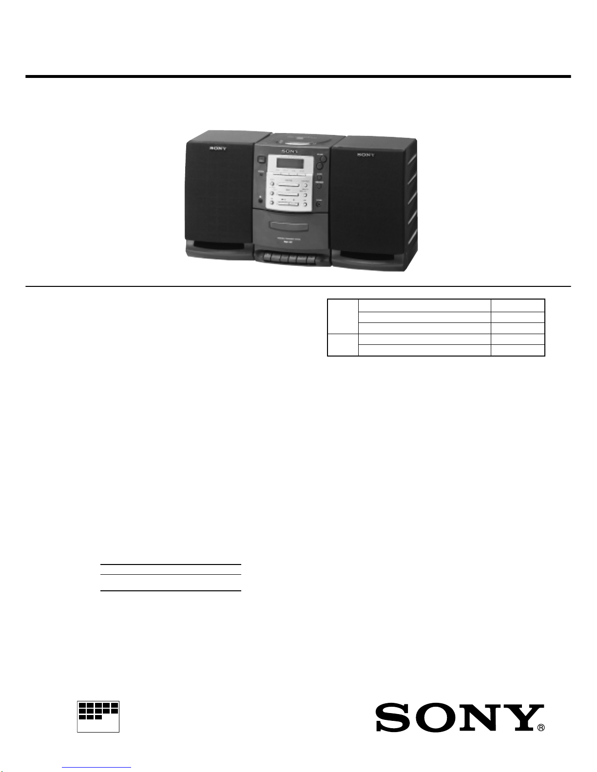
TABLE OF CONTENTS
1. GENERAL
Playing a CD ........................................................................... 4
Listening to the radio............................................................... 5
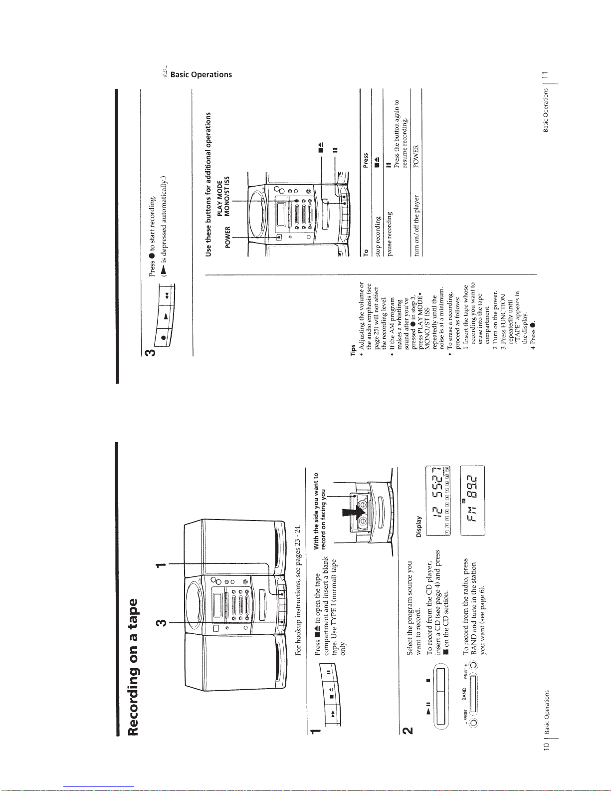
Playing a tape .......................................................................... 6
Recording on a tape ................................................................. 7
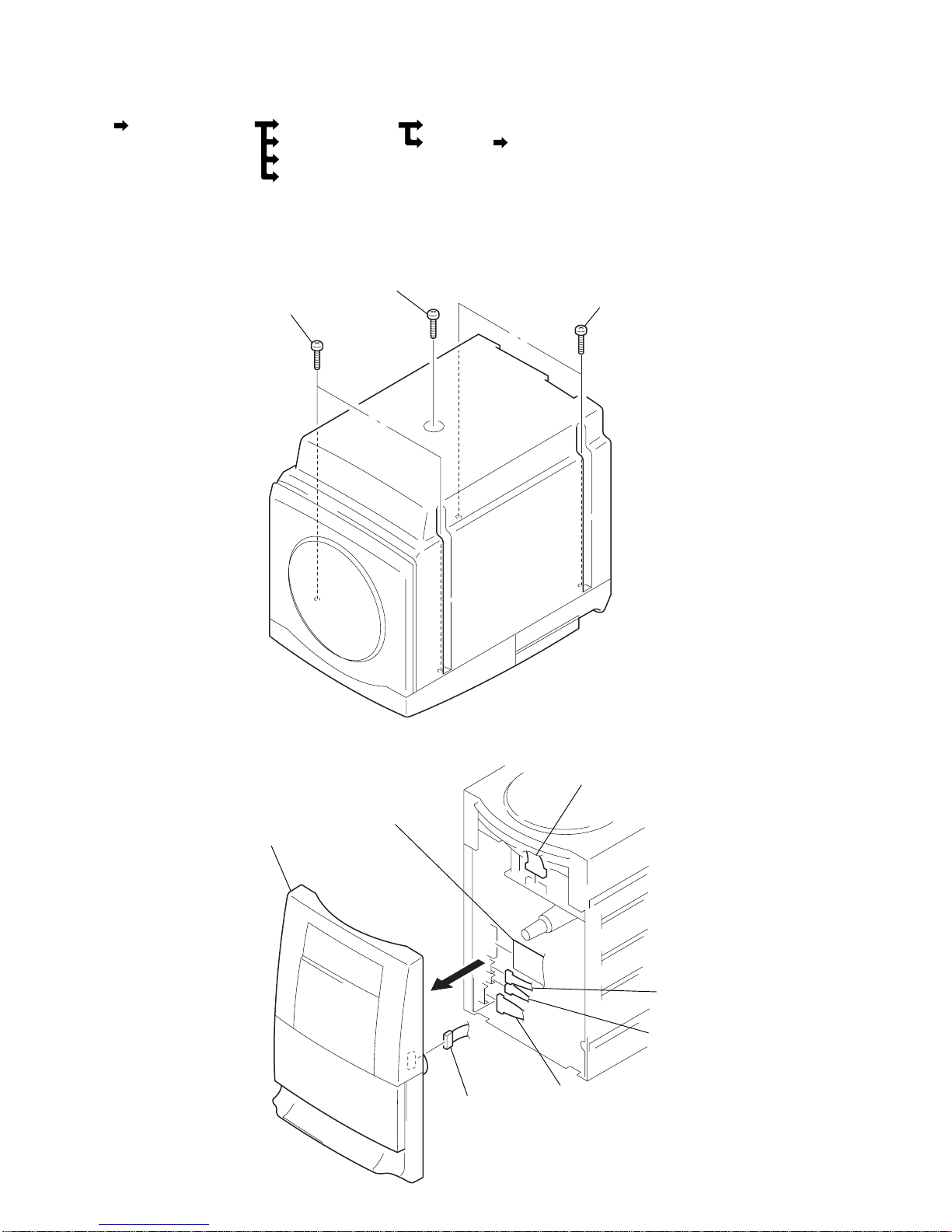
2. DISASSEMBLY
2-1. Front Cabinet Assy .............................................................. 8
2-2. CD Chassis Assy ................................................................. 9
2-3. Power Board ........................................................................ 9
2-4. Main Board ....................................................................... 10
2-5. CD Board .......................................................................... 10
2-6. Optical Pick-up ................................................................. 11
2-7. Mechanism Deck Block .................................................... 11
2-8. Control Board .................................................................... 12
3. MECHANICAL ADJUSTMENTS ............................... 13
4. ELECTRICAL ADJUSTMENTS
Tape Section .......................................................................... 13
Tuner Section......................................................................... 14
CD Section ............................................................................ 16
5. DIAGRAMS
5-1. IC Pin Description............................................................. 20
5-2. Circuit Boards Location .................................................... 22
5-3. Block Diagram –CD Section–........................................... 23
5-4. Block Diagram –Main Section–........................................ 25
5-5. Printed Wiring Boards –CD Section– ............................... 27
5-6. Schematic Diagram –CD Section–.................................... 29
5-7. Printed Wiring Boards –Main Section– ............................ 33
5-8. Schematic Diagram –Main Section (1/2)– ........................ 35
5-9. Schematic Diagram –Main Section (2/2)– ........................ 37
5-10. Printed Wiring Boards –Panel Section–............................ 40
5-11. Schematic Diagram –Panel Section– ................................ 42
6. EXPLODED VIEWS
6-1. Rear Cabinet Section......................................................... 48
6-2. Front Cabinet Section........................................................ 49
6-3. Upper Cabinet Section ...................................................... 50
6-4. Cassette Mechanism Section-1 ......................................... 51
6-5. Cassette Mechanism Section-2 ......................................... 52
6-6. Cassette Mechanism Section-3 ......................................... 53
6-7. Cassette Mechanism Section-4 ......................................... 54
6-8. Optical Pick-up Section .................................................... 55
6-9. Speaker Section ................................................................. 56
7. ELECTRICAL PARTS LIST ........................................ 57
SAFETY CHECK-OUT
After correcting the original service problem, perform the following
safety check before releasing the set to the customer:
Checkthe antenna terminals,metal trim,“metallized” knobs,screws,
and all other exposed metal parts forAC leakage. Check leakage as
described below.
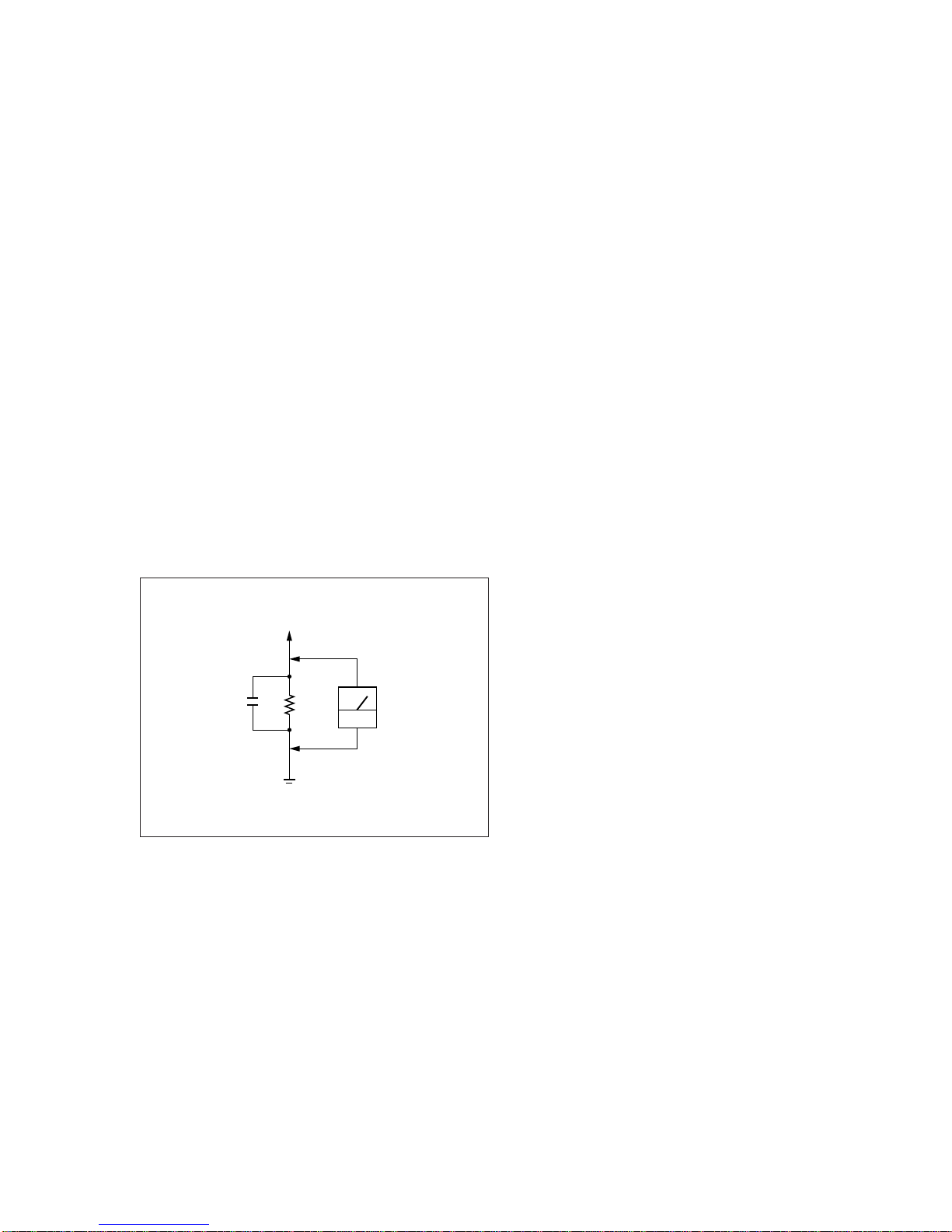
LEAKAGE TEST
The AC leakage from any exposed metal part to earth ground and
from all exposed metal parts to any exposed metal part having a
return to chassis, must not exceed 0.5 mA (500 microamperes).
Leakage current can be measured by any one of three methods.
1. A commercial leakage tester, such as the Simpson 229 or RCA
WT-540A. Follow the manufacturers’ instructions to use these
instruments.
2. A battery-operated AC milliammeter. The Data Precision 245
digital multimeter is suitable for this job.
3. Measuring the voltage drop across a resistor by means of aVOM
or battery-operatedAC voltmeter. The “limit” indication is 0.75
V, so analog meters must have an accurate low-voltage scale. The
Simpson 250 and Sanwa SH-63Trd are examples of a passive
VOM that is suitable. Nearly all battery operated digital
multimeters that have a 2V AC range are suitable. (See Fig. A)
Fig. A. Using an AC voltmeter to check AC leakage.
To Exposed Metal
Parts on Set
1.5k
Ω
0.15
µ
FAC
voltmeter
(0.75V)
Earth Ground


 User manual")