Sony HCD-101 User manual

HCD-101
AEP Model
UK Model
E Model
Tourist Model
SERVICE MANUAL
COMPACT COMPONENT SYSTEM
MICROFILM
Model Name Using Similar Mechanism NEW
CD Mechanism Type CDM50
Optical Pick-Up Type KSS-313A
SPECIFICATIONS
— Continued on next page —
• HCD-101 is the CD PLAYER,
TUNER and AMPLIFIER
sections in CMT-101.
Tuner section
Tuning range
2 band model
European model: FM : 87.5-108MHz
(50kHz step)
AM : 522–1,611kHz
Other models: FM : 87.5–108MHz
(50kHz step)
AM : 531–1,602kHz
(at 9kHz interval)
530–1,710kHz
(at 10kHz interval)
3 band model FM : 87.5–108MHz
(50kHz step)
MW : 522–1,611kHz
(at 9kHz interval)
LW : 144–288kHz
(at 3kHz interval)
Intermediate frequency FM : 10.7MHz
AM : 450kHz
Aerial terminals FM : 75Ωunbalanced
AM : External aerial
terminal
Timer Quartz lock system
Timer setting One-minute step
Sleep timer 10–minute step, max.
90minutes
CD player section
System Compact disc digital
audio system
Laser Semiconductor laser
(λ=780nm)
Laser output power Less than 44.6µW*
* This output is the value measured at a distance of 200mm from
the objective lens surface on the optical pick-up block with 7mm
aperture.
Frequency response 5Hz–20kHz
Signal to noise ratio More than 90dB
Harmonic distortion Less than 0.05%
Amplifier section
European model:
DIN power output 15+15 W (4Ωat 1kHz, DIN
Continuous RMS power output
21+21 W (4Ωat 1kHz, 10%
THD)
Music power output 26+26 W
Other model
Rated RMS power output16+16 W (4Ωat 1kHz, 1% THD,
AC240V/AC120V)
Reference RMS power output
22+22 W (4Ωat 1kHz, 10% THD,
AC240V/AC120V)
Inputs VIDEO/PC IN jack : Stereo
phone jack, sensitivity 500mV,
impedance 47kΩ

— 2 —
SAFETY-RELATED COMPONENT WARNING!!
COMPONENTS IDENTIFIED BY MARK !OR DOTTED LINEWITH
MARK !ON THE SCHEMATIC DIAGRAMS AND IN THE PARTS
LIST ARE CRITICAL TO SAFE OPERATION. REPLACE THESE
COMPONENTS WITH SONY PARTS WHOSE PART NUMBERS
APPEAR AS SHOWN IN THIS MANUAL OR IN SUPPLEMENTS
PUBLISHED BY SONY.
TABLE OF CONTENTS
1. GENERAL ······································································ 3
2. DISASSEMBLY
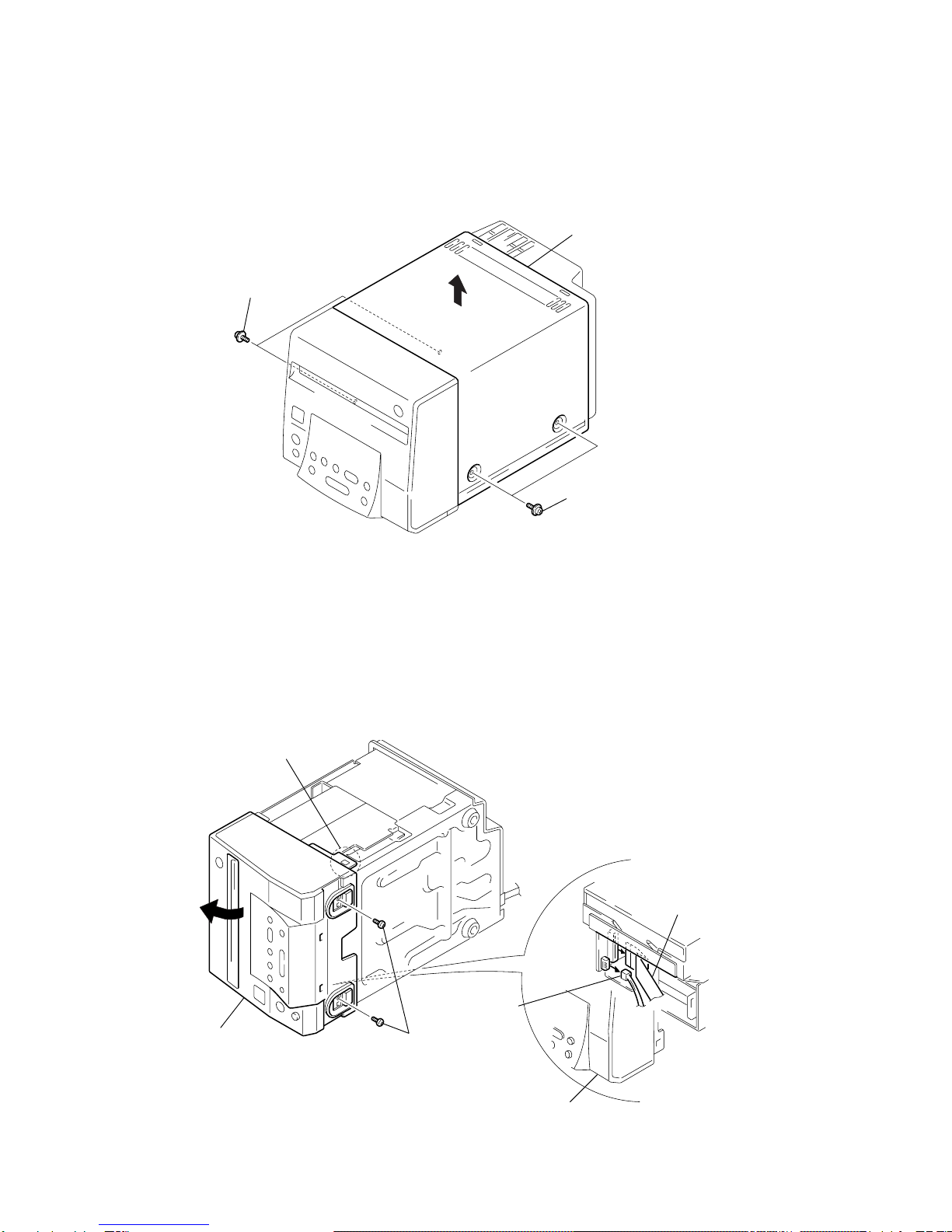
2-1. Case ···················································································· 4
2-2. Front Panel Section ···························································· 4
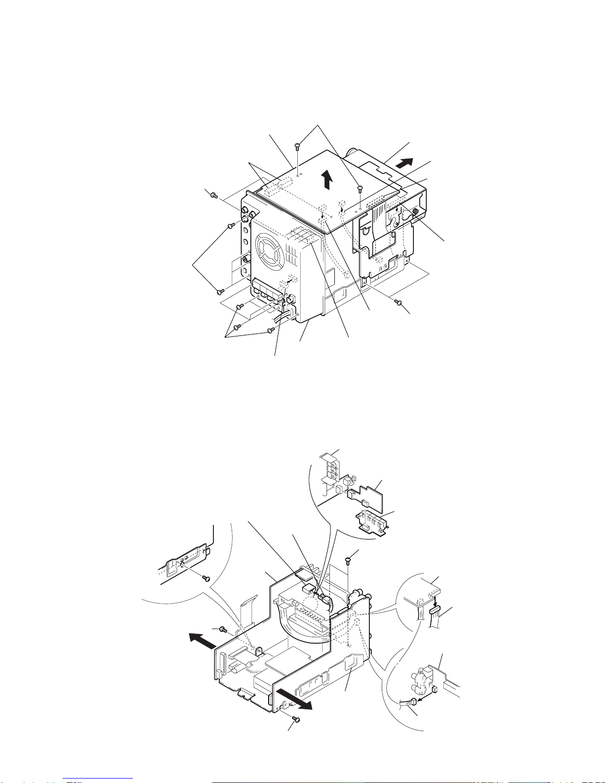
2-3. PRE Board ·········································································· 5
2-4. Function board, Relay board, SP TM board, Trans board,
Power board········································································ 5
2-5. Mechanism Deck ································································ 6
2-6. Chassis (T2) Assy ······························································· 6
2-7. BD Board············································································ 7
2-8. Roller Arm Block Assy······················································· 7
2-9. Chassis (OPT), Chucking Arm Assy ·································· 8
2-10. Motor (SL) Assy (M102), Optical Pick-Up························ 8
3. TEST MODE ·································································· 9
4. ELECTRICAL ADJUSTMENT ······························ 11
5. DIAGRAMS
5-1. Circuit Boards Location ··················································· 14
5-2. Block Diagram ································································· 15
5-3. Schematic Diagram –BD Section– ··································· 18
5-4. Printed Wiring Board –BD Section– ································ 21
5-5. Printed Wiring Board –Panel Section–····························· 23
5-6. Schematic Diagram –Panel Section – ······························ 25
5-7. Printed Wiring Board –PRE Section– ······························ 27
5-8. Schematic Diagram –PRE Section– ································· 29
5-9. Printed Wiring Board –Function Section– ······················· 31
5-10. Schematic Diagram –Function Section– ·························· 33
5-11. Printed Wiring Board –Power Section– ··························· 36
5-12. Schematic Diagram –Power Section– ······························ 39
5-13. IC Pin Function ································································ 42
5-14. IC Block Diagrams ··························································· 44
6. EXPLODEDVIEWS
6-1. Front Panel Section ·························································· 47
6-2. Chassis Section ································································· 48
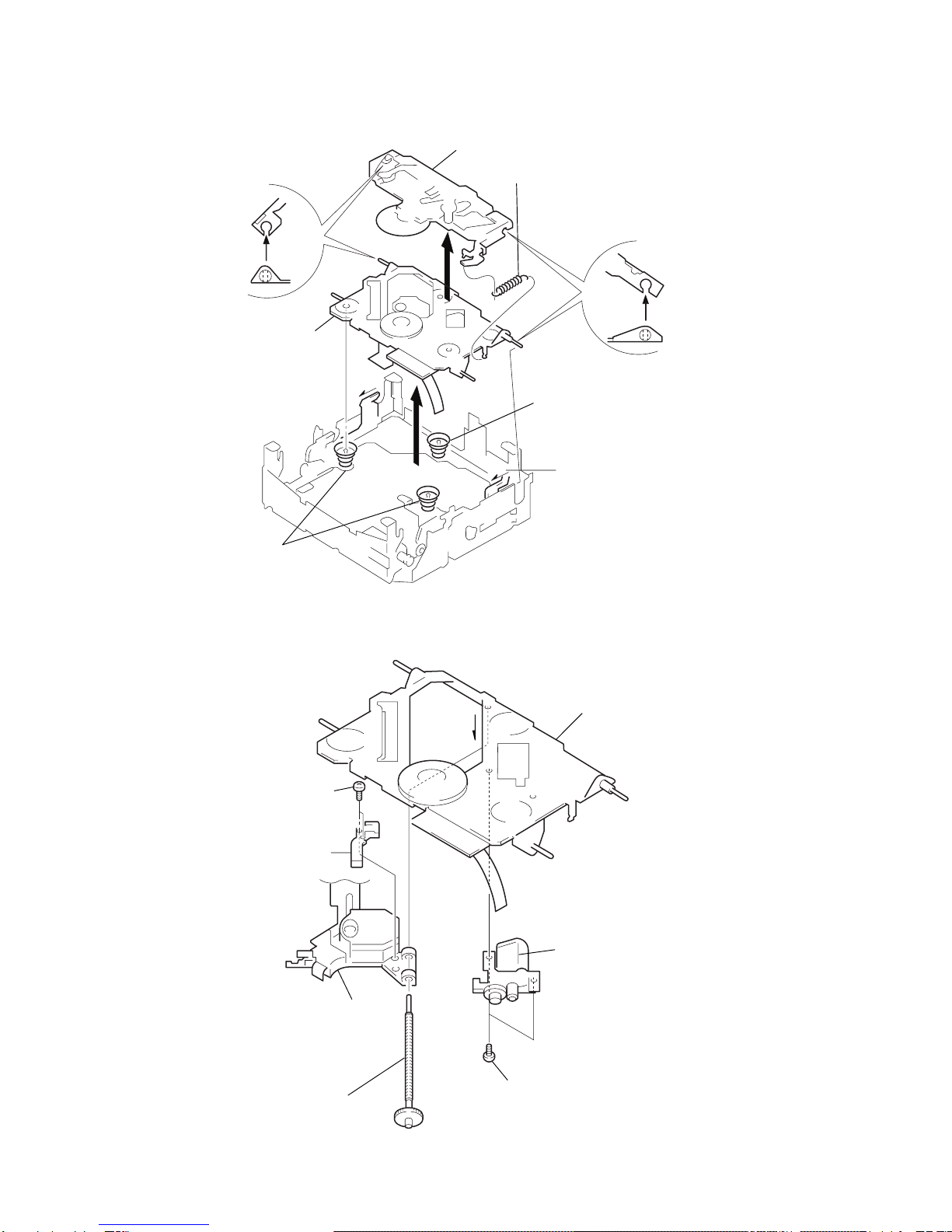
6-3. Mechanism Deck Section-1 (CDM50)····························· 49
6-4. Mechanism Deck Section-2 (CDM50)····························· 50
7. ELECTRICAL PARTS LIST ··································· 51
Outputs VIDEO/PC OUT jack : Stereo phone
jack, 250mV, 1kΩ
DIGITAL OUT (CD OPTICAL OUT):
Square optical connector jack, –18dBm,
wave jength 660nm
PHONES (headphones) jack :
Stereo mini jack, accepts head phones of
8Ωor more.
General
Power requirements
European model 220–230V AC, 50/60Hz
Other models 110–120V or 220–240V
AC, 50/60Hz adjustable
with voltage selector
Power consumption 66W (when connected to TC-TX101,
MDS-MX101)
Dimensions Approx. 142×125×260mm (w/h/d) incl.
projecting parts and controls
Mass Approx. 4.1kg
NOTES ON HANDLING THE OPTICAL PICK-UP
BLOCK OR BASE UNIT
The laser diode in the optical pick-up block may suffer electrostatic
break-down because of the potential difference generated by the
charged electrostatic load, etc. on clothing and the human body.
During repair, pay attention to electrostatic break-down and also
use the procedure in the printed matter which is included in the
repair parts.
The flexible board is easily damaged and should be handled with
care.
NOTES ON LASER DIODE EMISSION CHECK
The laser beam on this model is concentrated so as to be focused on
the disc reflective surface by the objective lens in the optical pick-
up block. Therefore, when checking the laser diode emission,
observe from more than 30 cm away from the objective lens.
Notes on chip component replacement
•Never reuse a disconnected chip component.
•Noticethattheminus side of atantalumcapacitormay be damaged
by heat.
Flexible Circuit Board Repairing
•Keep the temperature of soldering iron around 270 ˚C during
repairing.
•Do not touch the soldering iron on the same conductor of the
circuit board (within 3 times).
•Be careful not to apply force on the conductor when soldering or
unsoldering.
SERVICE NOTE

— 3 —
SECTION 1
GENERAL This section is extracted
from instruction manual.
1Remote control signal sensor
2Power switch
3CD insertion slot
4Display window
56(CD EJECT) button
6PHONES terminal
7BAND button
8DBFB button
9=0/)+ (Cue-up musics, or fast rewind / fast
forward) button
0VOL+/– button
!¡ ^(CD playback or pause) button
!™ FUNCTION button
!£ p(CD stop) button

— 4 —
SECTION 2
DISASSEMBLY
2-1. CASE
1
Two screws (Case 3 TP2)
1
Two screws (Case 3 TP2)
2
Remove the case upward in the
direction of the arrow.
2-2. FRONT PANEL SECTION
3
Wire (Flat Type)
(27 Core)
5
Front panel section
4
Connector
(CN916)
1
Two screws
(BV/Ring S Tight)
2
Pull the front panel out.
claw

— 5 —
2-3. PRE board
9
Wire (Flat type) (21 Core)
(CN421)
7
Connector (CN107)
!™
PRE board
!¡
Two Connectors
(CN420, CN422)
4
Two screws (BVTP 3
×
8)
8
CDM50
6
Wire (Flat type)
(30 Core)
5
Two screws
(BVTT 3
×
6)
3
Back Panel
2
Connector
(CN814)
!º
Connector
(CN423)
!£
Remove CN911
6-pin (Posistor board)
1
Four screws
(BVTP 3
×
8)
1
Six screws
(BVTP 3
×
8)
5
Two screws
(BVTT 3
×
6)
2-4. FUNCTION board, RELAY board, SP TM board, TRANS board, POWER board
8
Two screws (BVTT 3
×
6)
6
Relay board
7
SP TM board
!¡
Trans board
Power board
!º
Power cord (CN902)
9
Power board
3
Connector (CN910)
Trans board
Function board
2
Connector (CN404)
4
Function board
1
Screws (BVTP 3
×
8)
5
Screws
(BVTP 3
×
8)

— 6 —
2-5. MECHANISM DECK (CDM50)
3
Mechanism Deck (CDM50)
2
Bracket (CDM)
1
Two screw (BVTT 2.6
×
6)
1
Two screw (BVTT 2.6
×
6)
2-6. CHASSIS (T2) ASSY
5
Tension coil spring
3
Four screws
(BVTT 3
×
6)
6
Chassis (T2) assy
1
Two screws
(BVTT 2.6
×
6)
2
Bracket
4
Sensor Flexible
board

— 7 —
2-7. BD board
3
Flexible board
(CN106)
4
Flexible board
(CN101)
2
Connectir (CN104)
1
Two screws
(BVTT
×
2)
5
BD board
2
BELT (L
)
1
Spring (press)
3
Roller arm block assy
1
Spring (press)
2-8. ROLLER ARM BLOCK ASSY

— 8 —
2-9. CHASSIS (OPT) ASSY, CHUCKING ARM ASSY
6
Move the Chucking arm assy
to the position shown in the
illustration and move it up.
6
Move the Chucking arm assy
to the position shown in the
illustration and move it up.
5
Spring (CH)
7
Chucking arm assy
4
Spring (FL2)
1
Move the lever in the
direction of arrow (A).
A
3
Two Spring (FL)
2
Chassis (OPT)
assy
2-10. MOTOR (SL) ASSY (M102), OPTICAL PICK-UP (KSS-313A)
A
3
Move the shift (SL)
assy in the direction
of arrow
A
remove
it from chassis (OPT)
and optical Pick-up.
7
Chassis (OPT) assy
4
Screws
(+P 1.7
×
4)
5
Gear (SL Feed)
6
Optical Pick-Up
(KSS-313A)
1
Two screws (+BVTT 3
×
6)
2
Motor (SL)assy (M102
)

— 9 —
There are two methods to enter the TEST mode.
• How to Enter the Test Mode - 1
Remove theAC power cord from wall outlet, and press [EJECT
6]. While pressing [EJECT 6], connect the AC power cord to
wall outlet.
• How to Enter the Test Mode - 2
(This method toggles between “Entering the TEST Mode” and
“Exiting the TEST Mode”.)
Turn on the main power. While pressing [TUNING +], press
[DBFB], release hand from [DBFB] then press [FUNCTION].
(Keep pressing [TUNING] all the way.)
Pressing these buttons again in the same order exits the TEST
mode.
* The small ATT segment lights in the center top of display during
the TEST mode.
* To exit the TEST mode, disconnect theAC power cord from wall
outlet, or use “How to Enter the TEST Mode - 2”.
1. Audio volumecontrol setting (Canbeadjustedonly duringTEST
mode.)
Press [CD STOP p] and [VOL–] at the same time
→VOL MINIMUM appears
Press [CD STOP p] and [VOL+] at the same time
→VOL MAXIMUM appears
* The audio volume data is kept stored even after the main power
is turned off.
2. Audio balance setting (Can be adjusted only during TEST
mode.)
Press [CD STOP p] and [DBFB] at the same time
→LEFT 10 appears
Press [CD STOP p] and [FUNCTION] at the same time
→RIGHT 10 appears
Press [CD STOP p] and [CD EJECT 6] at the same time
→CENTER appears
* The audio balance data is kept stored even after the main power
is turned off.
3. Key test and FL display tube test (Can be adjusted only during
TEST mode.)
• Press [VOL-] and [BAND] at the same time→All FL tubes
light. Pressing the following key in this status enables key
checks as follows.
• Display depending upon the pressed key
[FUNCTION] →KEY NO. 1
[VOL –] →KEY NO. 2
[VOL +] →KEY NO. 3
[BAND] →KEY NO. 4
[TUNING+] →KEY NO. 5
[EJECT 6]→KEY NO. 6
[TUNING –] →KEY NO. 7
[STOP p]→KEY NO. 8
[PLAY ^]→KEY NO. 9
[DBFB] →KEY NO. 10
• [POWER] →Returns to the TEST mode
* Note: After all keys are (KEY No.1 to KEY No.10) tested,
CHECK OK!! appears.
The following items have no relation with the TEST mode.
4. Initial setting (All clear of all memories)
Disconnect the AC power cord. While pressing [POWER],
connect the AC power cord to wall outlet.
5. Watch operation check (Can be operated only while the main
power is off.)
Press [FUNCTION] and [BAND] at the same time. →Watch
starts counting.
Various CD tests
Pressing the two keys at the same time enables the various
adjustment and test as follows in the TEST mode, and “ATT”
segment is flashing.
1) Pressing [TUNING–] and [CD EJECT 6] at the same time :
The present normal tracking balance value (“31” to “36”) is
displayed when the above key operation is performed and
(TRBAL.) is displayed.
The tracking gain is fixed to “3F” (TOG1 to TOG2: all off)
2) Pressing [TUNING–] and [DBFB] at the same time :
(SHUFFLE) is displayed.
• ADJUSTMENT mode
When the above key operation is performed, the machine
enters the ADJUSTMENT mode. The “SHUFFLE” flashes
on display tube.
During the ADJUSTMENT mode:
The CLV gain is not switched to 8 cm. (The CLV gain is
fixed to 12 cm always.)
The machine is ready to enter theAF-ADJUSTMENT mode
as described below.
3) Pressing [TUNING–] and [FUNCTION] at the same time :
(SHUFFLE) and (PROGRAM) are displayed.
• AF-ADJUSTMENT mode
After the machine enters the ADJUSTMENT mode by the
key operation as described in step 2), the machine can enter
the AF-ADJUSTMENT mode by pressing the above key
operation. [TUNING – /FUNCTION]
The “SHUFFLE” and “PROGRAM” flash on display.
During theAF-ADJUSTMENT mode, the tracking and sled
servos are turned off in addition to theADJUSTMENT mode.
The machine stops the GFS error check which is normally
performed by software.
• Sled motor check
When disc is removed by pressing EJECT during the AF-
ADJUSTMENT mode, the sled can be moved to inner
circumferenceoroutercircumference by pressing [TUNING–
] or [TUNING+]. At this time, because the microprocessor
is not sensing the sled position, be careful when moving the
sled not to damage gears and other mechanism.
4) Pressing [TUNING–] and [VOL–] at the same time :
• No CDM mode
[1] is displayed.
When the above key operation is performed, the control on
the slot mechanism which takes in and ejects a CD disc is
stopped.
At this time “1” on the display flashes.
During the no CDM mode,
The TOC data is deleted by the [CD EJECT 6] key.
(When the TEST mode is cleared and a CD disc is inserted,
machine reads the TOC again.)
SECTION 3
TEST MODE

— 10 —
5) Pressing [TUNING–] and [VOL+] at the same time :
• Aging mode
The machine enters the aging mode by inserting a CD disc
and performing the above button
operation. The display starts counting the aging operation
with COUNT display, and “REPEAT” flashes.
Aging operation
1. Machine takes a disc into the machine.
2. Reads the TOC.
3. Accesses to the last track.
4. Plays back the last 2 seconds.
5. Ejects the disc.
The one complete operation from step 1 to step 5 is one count.
The cycle is repeated. However, steps 2 to 4 are skipped in all
modes other than the CD function.
Steps 1 and 5 are skipped in the no CDM mode.
The aging operation ends when an error occurs.
Aging error display
“Load Error” : Loading operation is not completed in four
seconds.
“Eject Error” : Eject operation is not completed in four
seconds.
“Q TOC Err” : The Q data could not be read during eight
seconds. (During TOC read)
“Q SRCH Err” : The Q data could not be read during eight
seconds. (During track search)
“Q PLAY Err” : The Q data could not be read during eight
seconds. (During PLAY)
“FOK UP Err” : Focus could not be locked in. (During
setup)
“FOK TOC Err” : Focus is un-locked many times. (During
TOC read)
“FOK SRCH Err” : Focus is un-locked many times. (During
track search)
“FOK PLAY Err” : Focus is un-locked several times. (During
play)
“GFS UP Err” : GFS error. (During setup)
“GFS TOC Err” : GFS error. (During TOC read)
“GFS PLAY Err” : GFS error. (During play)
Display selection during aging
The display can be switched by pressing the [TUNING–] and
[FUNCTION] at the same time :
Count display
Elapsed time display
Other errors
Normal display
Example of display
" COUNT 723 " (Machine has repeated for 723 times.)
" 12 : 05 : 35 " (12 hours 5 minutes 35 seconds have elapsed.)
" TW 2 SW 1 "
** Other troubles
“TW*SW*”
TW : Numbers of times that the machine could not read
TOC.
SW : Numbers of times that the machine could not
complete the track search within 16 seconds.
To exit the aging mode and to return the TEST mode, press
[TUNING – ] and [VOL +] at the same time.

— 11 —
CD SECTION
Note:
1. CD Blockisbasicallyconstructedto operate without adjustment.
Therefore, check each item in order given.
2. UseYEDS-18 disc (3-702-101-01) unless otherwise indicated.
3. Use the oscilloscope with more than 10MΩimpedance.
4. Clean an object lens by an applicator with neutral detergent
when the signal level is low than specified value with the
following checks.
5. When optical pickupisreplacedduringrepair, perform the focus
bias adjustment.
Focus Bias Adjustment
This adjustment is to be done when the optical block is replaced.
Adjustment procedure:
1. Connect oscilloscope to test point TP (VC) and TP (RF) on BD
board.
2. Turned power switch ON. (Stop state)
3. Insert disc (YEDS-18) and press the ^button.
4. Adjust RV101 so that the oscilloscope waveform is as shown in
the figure below (eye pattern).
A good eye pattern means that the diamond shape (≈) in the
center of the waveform can be clearly distinguished.
•RF signal reference waveform (eye pattern)
When observing the eye pattern, set the oscilloscope for AC
range and raise vertical sensitivity.
S-Curve Check
Procedure:
1. Connect as oscilloscope to test point TP (VC) andTP (FEO) on
BD board.
2. Connect a lead wire between test point TP (FOK) and Ground.
3. Turned Power switch on.
4. Insert disc (YEDS-18) and turned Power switch on again to
actuate the focus search. (actuate the focus search when disc
table is moving in and out.)
5. Check the oscilloscope waveform (S-curve) is symmetrical
betweenA and B.And confirm that peak to peak level is within
2.4 ± 0.7 Vp-p.
S-curve waveform
+
–
BD board
TP (RF)
TP (VC)
oscilloscope
(DC range)
VOLT/DIV: 200 m
V
TIME/DIV: 500 ns
level:
1.3
±
0.3Vp-p
+
–
BD board
TP (FEO)
TP (VC)
oscilloscope
A
B
symmetry
within 2.4
±
0.7 Vp-p
+
–
BD board
TP (RF)
TP (VC)
oscilloscope
VOLT/DIV: 200 m
V
TIME/DIV: 500 ns
level:
1.3
±
0.3Vp-p
+
–
BD board
TP (TEO)
TP (VC)
oscilloscope
(DC range)
SECTION 4
ELECTRICAL ADJUSTMENTS
6. After check, remove the lead wire connected in step 2.
Note: •Try to measure several times to make sure that the ratio of
A:B or B:A is more than 10:7.
•Select a longer sweep time and increase the brightness to
obtain best waveform.
RF Level Check
Procedure:
1. Connect oscilloscope to test point TP (VC) and TP (RF) on BD
board.
2. Turned Power switch on.
3. Insert the disc (YEDS-18) and press the ^button.
4. Confirm thatoscilloscopewaveformis clear and checkRFsignal
level is correct.
Note: Clear RF signal waveform means that the shape “≈” can be
clearly distinguished at the center of the waveform.
RF signal waveform
E-F Balance (Traverse) Check
Procedure:
1. Set up the TEST mode step 3) AF-ADJUSTMENT. (see page
9.)
2. Connect as oscilloscope to test point TP (TEO) on BD board.
3. Turned Power switch on.
4. Insert the disc (YEDS-18) in and press the ^button.
5. Confirm that the oscilloscope waveform is symmetrical on the
top and bottom in relation to 0V dc, and check the amplitude.

— 12 —
Focus/Tracking Gain Adjustment
This gain has a margin, so even if it is slightly off. There is no
problem.
Therefore, do not perform, RV102 and RV103 adjustment.
Please note that it should be fixed to mechanical center position
when you moved and do not know original position.
Adjustment Location:
[BD BOARD] — Component side —
A
B
0 V
specified value: amplitude: 300
±
100 mVp-p
×
100 = less than
±
7%
A-B
2 (A+B)
•
•
A+B = 300
±
100 mVp-p
Traverse waveform
symmetr
y
(VC)
(RF)
(PCK)
IC102
IC104
(FOK)
(A.GND)
(D.GND) (TEO)
(TEI)
RV101
RV102
RV103
(FEI)
(TAO)
(FEO)

— 13 —

— 14 —
SECTION 5
DIAGRAMS
5-1. CIRCUIT BOARDS LOCATION
PRE board
POWER IC board
POWER board
BD board
HP board
SENSOR board
SWITCH board
PANEL board
VOL SEL board
EJECT board
FUNCTION board
MOTOR board
SP TM board
RELAY board
TRANS board
RDS board
POSISTOR board

HCD-101
5-2. BLOCK DIAGRAM
— 15 — — 16 — — 17 —
FLUORESCENT
INDICATOR TUBE
CN410
J402
ANTENNA
1
FM
4
AM
19
ST-R
22
STEREO
21
TUNED
20
MUTE
9
DO
8
CL
6
CE
7
DI
17
ST-L 12
19
L OUT
E
TB401
TUNER UNIT
R-CH
J401
VIDEO/
1
1
CNJ401(1/3)
CNJ402(1/3)
5
4
15
14
2
1
15
PD1
11
A
10
B
9
C
3
IC401
INPUT SELECT
IC404(1/2)
BUFFER
IC430
BUFFER DBFB
689
R-CH
2
1
13
Q401
9V
IC422
SURROUND
SWITCH
REC OUT
SWITCH
IC402
CONTROL
Q421
SURROUND
SWITCH
12
14
11
10
35
13
9
AB
EFFECT
SWITCH
IC423
Q424
MUTE
MUTE
SWITCH
Q420,422 Q425
MUTE
L IN
18
CK
10
31
RFO
2
R OUT
R-CH
IC424
VOL LOUDNESS IC801
POWER AMP
STAND-BY
SWITCH
Q802,803 RELAY
DRIVE
Q804
STAND-BY
SWITCH
Q801
RY801
+
+
R-CH
R-CH
PHONES
SPEAKER
TM801
J660
2
2
J401(2/3)
J402(2/3)
TAPE
MD
OUT
STAND-BY
SWITCH
Q805
DELAY
IC802 3
1
D+5.6V
POWER ON
SWITCH
Q821
CUTOFF
SWITCH
Q820,822
ANA -9V
SIN
2
5
F.A
IC410
8BIT S/P CONV
6
F.B 7
F.C 16
SURR 14
F.A 15
F.B
9
AUB1 8
AUB2
13
ST POWER 10
CD POWER
CK
3
LAT
412
POW
LD DRIVE
Q101,102
AD
CB
F
K
B+
OPTICAL PICK-UP BLOCK
(KSS313A)
LASER ON
DIODE VR
FOCUS
COIL
TRACKING
COIL
2-AXIS
DEVICE
FCS+
FCS
TRK+
TRK
A
C
B
D
F
E
PD
LD
FOCUS
GAIN
TRACKING
GAIN
FOCUS
BIAS
RV102
RV103
RV101
PD2
36
F
38
E
39
LD
33
PHD
34
FEI
2
TEO
42
TEI
44
FEO
1
23
C OUT
21
DATA
24
SENS
20
XLT 19
CLK
25
FOK
37
FE BIAS
22
IC101
RF AMP,
FOCUS/TRACKING,
SLED SERVO
TRACKING
COIL
DRIVE
FOCUS
COIL
DRIVE
SLED
MOTOR
DRIVE
SPINDLE
MOTOR
DRIVE
FL701
9
R-CH
18
17
12
11
26
27
1
2
M
M
SLED
MOTOR
SPINDLE
MOTOR
SLED
M102
M101
14 15
16
19
25
4
7
MOTOR DRIVE
TRACKING/FOCS
COIL DRIVE
SLED/SPINDLE
IC102
XRESET
TAO
13
FEO
6
FEM
7
SLO
16
TAM
12
SLM
15
IC103
DIGITAL SIGNAL
PROCESSOR
RF
14
CN IN
55
SE IN
54
FOK
1
DATAO
56
XLTO
57
CLKO
59
MDP
3
SPOD
63
S101
LIMIT SW
21
PCMD
22
BCLK 20
LRCK
34
XTAI 6
XTO
DATA
2
BCLK
3
LRCK
1
CKO
4
16
L OUT
13
R OUT
5
XTI
28
MLAT 27
CLOK 26
DATA
IC104
DIGITAL FILTER
D/A CONVERTER
X101
16.9344MHz
51
DATA 53
CLOK
52
XLAT
39
D OUT
11
XRST
XRST
XRST
50
47
SQCK
43
SCOR 52
SQSO 46
49
SENS
STB
12
DATA
11
IC701
SYSTEM CONTROL
TA MUTE
47
TA DATA
6
TA CLOCK
7
SP LATCH
8
ST D OUT
3
ST CE
5
ST CLK
4
ST D IN
45
TU MUTE
50
TUNED
43
STEREO
44
2
AU BUS OUT
DF LATCH
21
CD DATA
18
CD CLOCK
17
DSP LATCH
20
SQCLK
22
SCOR
36
SUBQ
24
SENS
19
9
7
M
LOADING
MOTOR
M103 2
4
LM2
LOAD IN
49
LOAD OUT
48
X1
12
IC105
LOADING MOTOR
DRIVE
LM1
X2
11
5MHz
X701
TA LATCH
939
AU BUS IN
41
SIRCS
Q404
8
6
4
5
9
3
AUB CONTROL
IC403
FAN
DRIVE
Q823,824
FAN
8
L
L
J402(3/3)
J401(3/3)
9
11
AUB
AC
AC
8
9
11
AUB
AC
AC
IC901
CD
DIGITAL OUT
3
2
1
AC
AC
SW+5V
1
3
REMOTE
CONTROL
RECEIVER
IC751
10
RESET Q701
RESET
SWITCH
38
AC CUT
27
DISC DET
IC850
RESET
NON
BACK-UP 5V
XT1
15
XT2
14
32.76kHz
X702
88
80
78
53
.
99
89
100
T0 Q701
BUFFER
F1 F2
T1
T11
S0
S34
26
DISC SET
32
KEY0
33
KEY1
S1
DISC SET
POWER
S2
DISC DET
S761 EJECT
S755 DBFB
S751 VOL
S752 VOL +
S753 FUNCTION
S754
PLAY/
S762 STOP
S763 REW/AMS
S764 FF/AMS
S765 BAND
S766
PAUSE
LOAD IN
49
LOAD IN
49
PLAY/PAUSE
D751
Q921
SWITCH
IC933
REG
F2
F1
AC
AC
3 1
D904
F901
AC IN
D903
D902
Malaysia, Singapore, Hong Kong,
Tourist MODEL
AEP, UK, German MODEL
D905
T901
IC932
REG
3 1
IC931
REG
3 1
Q924
SWITCH
IC941
REG
3 1
Q931
CD SW+5V
Q910,911
SWITCH
D901
D703
D704
L701
L901
POW B+
POW B-
SW D +5V
SW A +5V
CDP +7V
ST +12V
(TUNER)
D+5.6V
(IC701)
NON BACK-UP 5V
(IC701)
BACK-UP
(IC701)
ANA +9V
ANA -9V
D +5V
16
L
L
L
L
IN
OUT
PC
FM
AM
19
DET
2
16
4IC601
RDS
IC602
BUFFER
AEP,German,
UK MODEL
RDS DATA
42
RDS CLK
37
240V 120V
S901
: FM
: MD
: VIDEO/PC
: TAPE
SIGNAL PATH
: REC
: CD
: DIGITAL OUT
• R-CH : Same as L-CH
TAPE
MD
IN
OPTICAL


Table of contents
Other Sony Stereo System manuals

Sony
Sony HCD-RG40 User manual

Sony
Sony MHC-EC70 - Mini Hi-fi Component System User manual

Sony
Sony HCD-GT444 User manual

Sony
Sony CMT-BX3R User manual

Sony
Sony SRS-X7 Reference guide

Sony
Sony STR-DA3700ES Use and maintenance manual

Sony
Sony CMT-S40D User manual

Sony
Sony ZS-S4iP User manual

Sony
Sony HCD-LX7 User manual

Sony
Sony SRS-XB12 User manual

Sony
Sony CMT-SBT100 User manual

Sony
Sony LBT-D109CD User manual

Sony
Sony HCD-551 User manual

Sony
Sony MEX-N5100BT User manual

Sony
Sony MHC-GR8 User manual

Sony
Sony HCD-NXM2D User manual

Sony
Sony XDR-DS16iPN User guide

Sony
Sony WX-900BT User manual

Sony
Sony HCD-G2500 User manual

Sony
Sony SA-WMS225 User manual