Sony HCD-N455KW User manual

— 1 —
SERVICE MANUAL
Model Name Using Similar Mechanism HCD-D570/N355/N355K
CD Mechanism Type CDM37-5BD19
Base Unit Type BU-5BD19
Optical Pick-up Type KSS-213BA/S-N
Model Name Using Similar Mechanism HCD-V4500
Tape Transport Mechanism Type TCM-220WR2E
MICROFILM
CD
SECTION
SPECIFICATIONS
HCD-N455KW is the tuner, deck, CD
and amplifier section in LBT-N455KW.
TAPE
DECK
SECTION
HCD-N455KW
Thailand Model
COMPACT Hi-Fi
STEREO SYSTEM
— Continue on next page —
w
w
w
.
x
i
a
o
y
u
1
6
3
.
c
o
m
Q
Q
3
7
6
3
1
5
1
5
0
9
9
2
8
9
4
2
9
8
T
E
L
1
3
9
4
2
2
9
6
5
1
3
9
9
2
8
9
4
2
9
8
0
5
1
5
1
3
6
7
3
Q
Q
TEL 13942296513 QQ 376315150 892498299
http://www.xiaoyu163.com

— 2 —
CAUTION
Use of controls or adjustments or performance of procedures
other than those specified herein may result in hazardous
radiation exposure.
Notes on chip component replacement
• Never reuse a disconnected chip component.
• Notice that the minus side of a tantalum capacitor may be
damaged by heat.
Flexible Circuit Board Repairing
• Keep the temperature of soldering iron around 270˚C
during repairing.
• Do not touch the soldering iron on the same conductor of the
circuit board (within 3 times).
• Be careful not to apply force on the conductor when soldering
or unsoldering.
Laser component in this product is capable of emitting radiation
exceeding the limit for Class 1.
This appliance is classified as
a CLASS 1 LASER product.
The CLASS 1 LASER
PRODUCT MARKING is
located on the rear exterior.
This caution
label is located
inside the unit.
SAFETY-RELATED COMPONENT WARNING !!
COMPONENTS IDENTIFIED BY MARK !OR DOTTED LINE
WITH MARK !ON THE SCHEMATIC DIAGRAMS AND IN
THE PARTS LIST ARE CRITICAL TO SAFE OPERATION.
REPLACE THESE COMPONENTS WITH SONY PARTS
WHOSE PART NUMBERS APPEAR AS SHOWN IN THIS
MANUAL OR IN SUPPLEMENTS PUBLISHED BY SONY.
w
w
w
.
x
i
a
o
y
u
1
6
3
.
c
o
m
Q
Q
3
7
6
3
1
5
1
5
0
9
9
2
8
9
4
2
9
8
T
E
L
1
3
9
4
2
2
9
6
5
1
3
9
9
2
8
9
4
2
9
8
0
5
1
5
1
3
6
7
3
Q
Q
TEL 13942296513 QQ 376315150 892498299
http://www.xiaoyu163.com

— 3 —
TABLE OF CONTENTS
1. SERVICING NOTE ............................................................ 4
2. GENERAL ........................................................................... 4
3. DISASSEMBLY
3-1. Front Panel Assembly and Main Board ................................. 6
3-2. TC Mechanism Deck ............................................................. 6
3-3. CD Mechanism Deck ............................................................. 7
3-4. BU Bracket Assembly............................................................ 7
3-5. Disc Table .............................................................................. 8
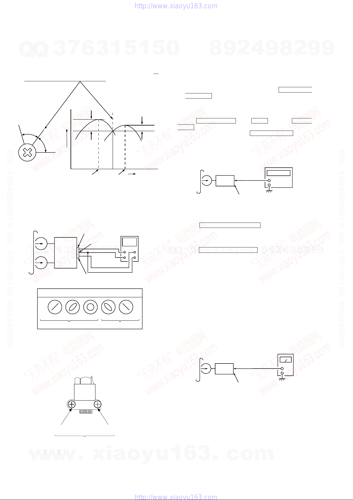
4. MECHANICAL ADJUSTMENTS ................................. 9
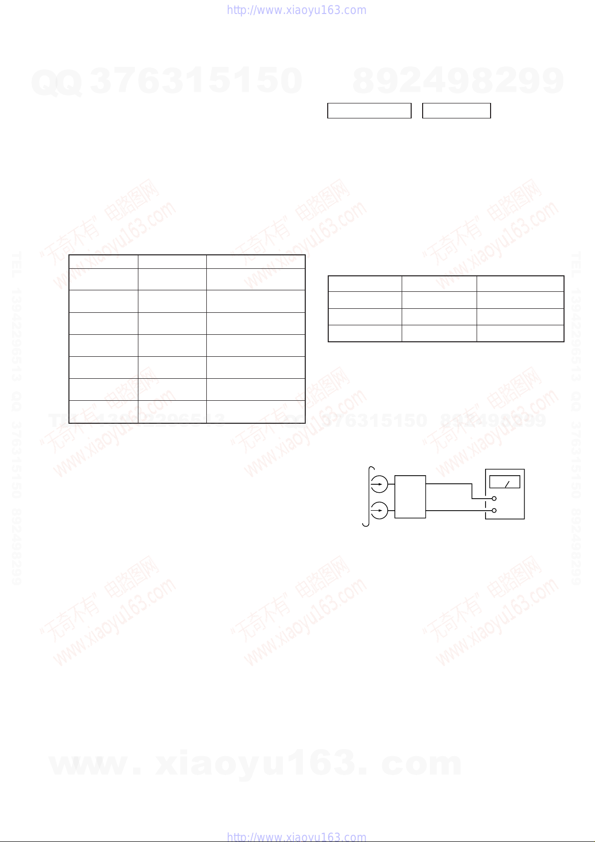
5. ELECTRICAL ADJUSTMENTS
DECK Section ............................................................................... 9
TUNER Section........................................................................... 12
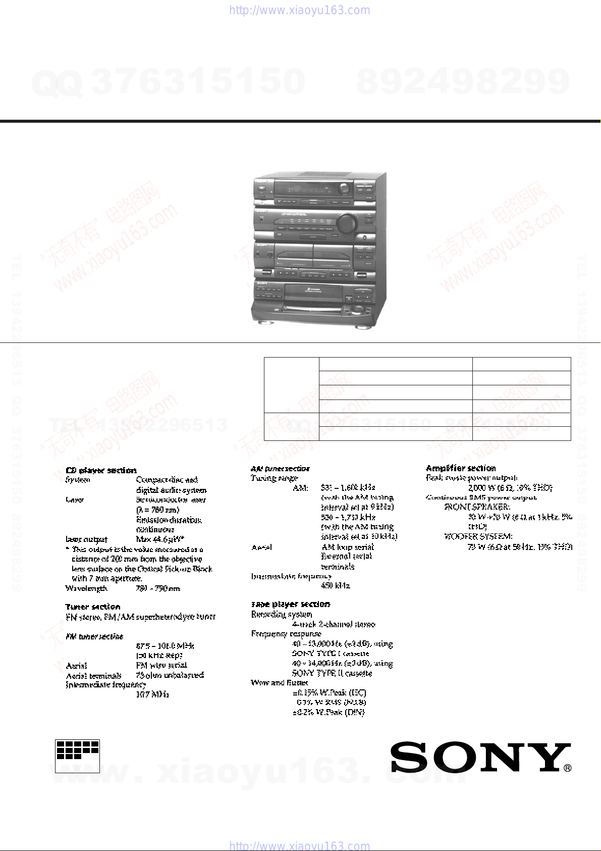
CD Section................................................................................... 13
6. DIAGRAMS
6-1. Block Diagrams
• Tuner Section ..................................................................... 15
• CD Section......................................................................... 17
• Deck Section...................................................................... 19
• Main Section...................................................................... 21
6-2. Circuit Boards Location ....................................................... 23
6-3. Printed Wiring Board — Tuner Section —.......................... 24
6-4. Schematic Diagram — Tuner Section —............................. 25
6-5. Printed Wiring Board — BD Section —.............................. 27
6-6. Schematic Diagram — BD Section — ................................ 29
6-7. Printed Wiring Board — Main Section —.......................... 33
6-8. Schematic Diagram — Main Section — ............................. 37
6-9. Schematic Diagram — Deck Section — ............................. 41
6-10. Printed Wiring Board — Deck Section — ......................... 45
6-11. Printed Wiring Board — Key Con Section — ................... 47
6-12. Schematic Diagram — Key Control Section — ................ 47
6-13. Printed Wiring Board — CD Motor Section —................. 49
6-14. Schematic Diagram — CD Motor Section —.................... 50
6-15. Printed Wiring Board — CD Panel Section — .................. 52
6-16. Schematic Diagram — CD Panel Section —..................... 53
6-17. Schematic Diagram — ST SW Section — ........................ 55
6-18. Printed Wiring Board — ST SW Panel Section —............ 57
6-19. Schematic Diagram — Panel Section — ........................... 59
6-20. Printed Wiring Board — Panel Section — ........................ 63
6-21. IC Block Diagrams............................................................. 67
6-22. IC Pin Functions
• IC501 Display Control (ASD0204GF-012-3BA)/
Panel board...................................................................... 72
• IC701 Master Control (TMP87CS64YF-6521)............... 73
7. EXPLODED VIEWS
7-1. Cabinet and Back Panel Section .......................................... 76
7-2. Panel Board Section ............................................................. 77
7-3. Front Panel Section .............................................................. 78
7-4. Chassis Section .................................................................... 79
7-5. TC Mechanism Section 1 (TCM-220WR2E) ...................... 80
7-6. TC Mechanism Section 2 (TCM-220WR2E) ...................... 81
7-7. TC Mechanism Section 3 (TCM-220WR2E) ...................... 82
7-8. CD Mechanism Section (CDM37-5BD19).......................... 83
7-9. Base Unit Section (BU-5BD19)........................................... 84
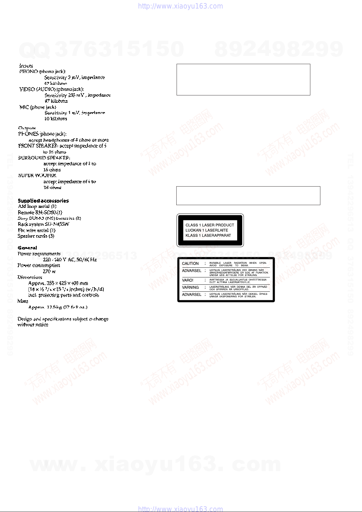
8. ELECTRICAL PARTS LIST ......................................... 85
w
w
w
.
x
i
a
o
y
u
1
6
3
.
c
o
m
Q
Q
3
7
6
3
1
5
1
5
0
9
9
2
8
9
4
2
9
8
T
E
L
1
3
9
4
2
2
9
6
5
1
3
9
9
2
8
9
4
2
9
8
0
5
1
5
1
3
6
7
3
Q
Q
TEL 13942296513 QQ 376315150 892498299
http://www.xiaoyu163.com

— 4 —
NOTES ON HANDLINGTHE OPTICAL PICK-UP BLOCK
OR BASE UNIT
The laser diode in the optical pick-up block may suffer electrostatic
break-down because of the potential difference generated by the
charged electrostatic load, etc. on clothing and the human body.
During repair, pay attention to electrostatic break-down and also use
the procedure in the printed matter which is included in the repain
parts.
The flexible board is easily damaged and should be handled with
care.
NOTES ON LASER DIODE EMISSION CHECK
The laser beam on this model is concentrated so as to be focused on
the disc reflective surface by the objective lens in the optical pick-up
block. Therefore, when checking the laser diode emission, observe
from more than 30 cm away from the objective lens.
LASER DIODE AND FOCUS SEARCH OPERATION CHECK
Carry out the “S curve check” in “CD section adjustment” and check
that the S curve waveform is output three times.
SECTION 1
SERVICING NOTE
FL Display Tube, LED All Lit and Key Check mode
When the TUNER/BAND , DISPLAY/DEMO , and FILE 2 but-
tons are pressed simultaneously, the FL display tube and LEDs will
all light up. Press any button to enter the key check mode.
When the key check mode is entered, the FL display tube displays
“K 1 J0 V0”. Each time a button is pressed, the counter increases in
the following order, K 2 nK 3 nK 4.
If buttons already pressed once are pressed again, the counter will
notincrease.When the VOLUME knobis rotated in the + direction,
the count increases in the following order.
V1 nV2 nV3.
When rotated in the – direction, it decreases in the following order.
V0 nV9 nV8.
When the AMS dial is rotated in the clockwise direction, the count
increases in the following order.
J1 nJ2 nJ3.
When rotated in the counterclockwise direction, it decreases in the
following order.
J0 nJ9 nJ8.
To exit form the test mode, press the TUNER/BAND , DISPLAY/
DEMO , FILE 2 buttons simultaneously again.
Switching the channel step 9 kHz/10 kHz
Press ENTER/NEXT button and SYSTEM POWER button simul-
taneously to switch theAM channel step 9 kHz and 10 kHz. Be sure
not to change with carelessness.
All Reset
When TUNER/BAND , DISPLAY/DEMO , and FILE3 buttons
are pressed simultaneously, the contents of a preset are restored to
those at shipping.
SECTION 2
GENERAL This section is extracted from
instruction manual.
w
w
w
.
x
i
a
o
y
u
1
6
3
.
c
o
m
Q
Q
3
7
6
3
1
5
1
5
0
9
9
2
8
9
4
2
9
8
T
E
L
1
3
9
4
2
2
9
6
5
1
3
9
9
2
8
9
4
2
9
8
0
5
1
5
1
3
6
7
3
Q
Q
TEL 13942296513 QQ 376315150 892498299
http://www.xiaoyu163.com

— 6 —
SECTION 3
DISASSEMBLY
Note : Follow the disassembly procedure in the numerical order given.
3-1. FRONT PANEL ASSEMBLY AND MAIN BOARD
3-2.TC MECHANISM DECK
1
Push the eject button.(two positions)
1
Remove the connectors.
• Main board (Six connectors)
• ST SW board (Four connectors)
• AMPLIFIER board (One connector)
• TRANS board (One connector)
3
Wire
2
Screw (BVTT 3x6)
6
Screw (BVTP 3x8)
7
Two screws (BVTP 3x8)
9
Main board
4
Three screws
(BVTP 3x8)
5
Front panel
assembly CN201 CN703
CN3103, CN3107,
CN3108
CN1604
CN3101
CN1204
8
Two screws
(BVTP 3x8)
CN203
CN402
CN702
CN401
2
Two cassette lids
Eject button
Eject button
5
Mechanism deck
3
Three screws
(BVTP 2.6x8)
4
Four screws
(BVTP 2.6x8)
w
w
w
.
x
i
a
o
y
u
1
6
3
.
c
o
m
Q
Q
3
7
6
3
1
5
1
5
0
9
9
2
8
9
4
2
9
8
T
E
L
1
3
9
4
2
2
9
6
5
1
3
9
9
2
8
9
4
2
9
8
0
5
1
5
1
3
6
7
3
Q
Q
TEL 13942296513 QQ 376315150 892498299
http://www.xiaoyu163.com

— 7 —
3-3. CD MECHANISM DECK
3-4. BU BRACKET ASSEMBLY
1
Screw (BVTP 3x8)
2
Two screws
(BVTP 3x8)
3
Two screws
(BVTP 3x8)
4
CD Mechanism
deck
2
BU bracket assembly
1
Yoke bracket
w
w
w
.
x
i
a
o
y
u
1
6
3
.
c
o
m
Q
Q
3
7
6
3
1
5
1
5
0
9
9
2
8
9
4
2
9
8
T
E
L
1
3
9
4
2
2
9
6
5
1
3
9
9
2
8
9
4
2
9
8
0
5
1
5
1
3
6
7
3
Q
Q
TEL 13942296513 QQ 376315150 892498299
http://www.xiaoyu163.com

— 8 —
3-5. DISCTABLE
Note :
When the Disc table is installed, adjust the positions
of Roller cam and mark ”as shown in the figure, then
set to the groove of disc table.
A
1
Screw (BVTP 3x8)
2
Screw (BVTP 3x8)
3
Bracket (BU)
4
Step screw
5
Disc table
A
w
w
w
.
x
i
a
o
y
u
1
6
3
.
c
o
m
Q
Q
3
7
6
3
1
5
1
5
0
9
9
2
8
9
4
2
9
8
T
E
L
1
3
9
4
2
2
9
6
5
1
3
9
9
2
8
9
4
2
9
8
0
5
1
5
1
3
6
7
3
Q
Q
TEL 13942296513 QQ 376315150 892498299
http://www.xiaoyu163.com

— 9 —
SECTION 4
MECHANICAL ADJUSTMENTS
Precaution
1. Clean the following parts with a denatured alcohol-moistened
swab:
record/playback heads pinch rollers
erase head rubber belts
capstan idlers
2. Demagnetize the record/playback head with a head demagnetizer.
3. Do not use a magnetized screwdriver for the adjustments.
4. After the adjustments, apply suitable locking compound to the
parts adjusted.
5. The adjustments should be performed with the rated power sup-
ply voltage unless otherwise noted.
Torque Measurement
SECTION 5
ELECTRICAL ADJUSTMENTS
DECK SECTION 0 dB=0.775V
1. Demagnetize the record/playback head with a head damagnetizer.
2. Do not use a magnetized screwdriver for the adjustments.
3. After the adjustments, apply suitable locking compound to the
parts adjusted.
4. The adjustments should be performed with the rated power sup-
ply voltage unless otherwise noted.
5. The adjustments should be performed in the order given in this
service manual. (As a general rule, playback circuit adjustment
should be completed before performing recording circuit adjust-
ment.)
6. The adjustments should be performed for both L-CH and R-CH.
7. Switches and controls should be set as follows unless otherwise
specified.
Record/Playback Head Azimuth Adjustment
(Deck A, Deck B)
Note: Perform this adjustments for both decks.
Procedure:
1. Mode : Playback
set
test tape
P-4-A100
(10kHz, –10dB) main board
CN403
Pin
3
(L-CH)
Pin
1
(R-CH)
level meter
main board
CN403
Pin
2
(GND)
+
–
2 to 6 g • cm
(0.02 - 0.08 oz • inch)
36 to 61 g • cm
(0.5 - 0.84 oz • inch)
Torque Torque meter Meter reading
FWD
FWD
back tension
REV
FF/REW
REV
back tension
FWD tension
REV tension
CQ-102C
CQ-102C
CQ-102RC
CQ-102RC
CQ-201B
CQ-403A
CQ-403R
36 to 61 g • cm
(0.5 - 0.84 oz • inch)
2 to 6 g • cm
(0.02 - 0.08 oz • inch)
61 to 143 g • cm
(0.85 - 1.99 oz • inch)
100 g or more
(3.53 oz or more)
100 g or more
(3.53 oz or more)
Signal Used forTape
Azimuth Adjustment
Tape Speed Adjustment
Level Adjustment
10 kHz, –10 dB
3 kHz, 0 dB
315 Hz, 0 dB
P-4-A100
WS-48B
P-4-L300
w
w
w
.
x
i
a
o
y
u
1
6
3
.
c
o
m
Q
Q
3
7
6
3
1
5
1
5
0
9
9
2
8
9
4
2
9
8
T
E
L
1
3
9
4
2
2
9
6
5
1
3
9
9
2
8
9
4
2
9
8
0
5
1
5
1
3
6
7
3
Q
Q
TEL 13942296513 QQ 376315150 892498299
http://www.xiaoyu163.com

— 10 —
2. Turn the adjustment screw and check output peaks. If the peaks
do not match for L-CH and R-CH, turn the adjustment screw so
that outputs match within 1 dB of peak.
output
level
3. Mode: Playback
Tape Speed Adjustment (Deck A)
Note: Start the Tape Speed adjustment as below after setting the test
mode.
The tape speed can be changed with the HIGH SPEED
DUBBING button during the test mode.
Method :
1. Turn the power switch on.
2. Pressthe DISPLAY/DEMO button, FILE 1 buttonand TUNER/
BAND button simultaneously.
To exit from the test mode, Press the SYSTEM POWER button.
Procedure :
Mode: Playback
4. After the adjustments, apply suitable locking compound to the
parts adjusted.
Adjustment Location: Playback Head (Deck A)
Record/Playback/Erase Head (Deck B)
45˚ 90˚ 135˚ 180˚
wronggood
in phase
R
set
FWD side REV side
L-CH
peak
screw
position
R-CH
peak
within
1dB within 1dB
L-CH
peak R-CH
peak
screw
position
test tape
P-4-A100
(10kHz, –10dB)
main board
CN403
Pin
3
(L-CH) oscilloscope
Pin
2
(GND)
L
Pin
1
(R-CH)
Waveform of oscilloscope
Adjustment screw
+
–
main board
CN403 Pin
3
(L-CH)
Pin
1
(R-CH)
set
test tape WS-48B
(3kHz, 0dB) frequency counter
1. Insert the WS-48B into the deckA to playback.
2. Press the HIGH SPEED DUBBING button. Then at HIGH
SPEED mode.
3. Adjust the RV652 on the AUDIO board so that the frequency
counter reading becomes 6,000 ± 30 Hz.
4. Press the HIGH SPEED DUBBING button again to be set the
NORMAL SPEED mode.
5. Set to the playback mode.
6. Adjust the RV651 on the AUDIO board so that the frequency
counter reading becomes 3,000 ± 15 Hz.
Frequency difference between deck A and deck B the beginning
of the tape should be within ± 1.5%.
Adjustment Location: AUDIO board
Playback Level Adjustment (Deck A, Deck B)
Procedure:
Mode: Playback
set
test tape P-4-L300
(315Hz, 0dB)
main board
CN403 Pin
3
(L-CH)
Pin
1
(R-CH)
level meter
Deck A is RV311 (L-CH) and RV411 (R-CH), deck B is RV301
(L-CH) and RV401 (R-CH)
so that adjustment within the following adjustment level.
Adjustment level:
CN403 playback level: 301.5 to 338.3 mV (–8.2 to –7.2 dB)
level difference between the channels: within ± 0.5 dB
Adjustment Location: AUDIO board
w
w
w
.
x
i
a
o
y
u
1
6
3
.
c
o
m
Q
Q
3
7
6
3
1
5
1
5
0
9
9
2
8
9
4
2
9
8
T
E
L
1
3
9
4
2
2
9
6
5
1
3
9
9
2
8
9
4
2
9
8
0
5
1
5
1
3
6
7
3
Q
Q
TEL 13942296513 QQ 376315150 892498299
http://www.xiaoyu163.com

— 11 —
Record Bias Adjustment (Deck B)
Procedure:
Reference)
When set to the test mode performed in Tape Speed Adjustment,
when the tape is rewound after recording, the “REC memory mode”
which rewinds only the recorded portion and stops is set.
This “REC memory mode” is convenient for performing this adjust-
ment.
1. Press FUNCTION button to select VIDEO.
2. Mode: record
Record Level Adjustment (Deck B)
Procedure:
Reference)
When set to the test mode performed in Tape Speed Adjustment,
when the tape is rewound after recording, the “REC memory mode”
which rewinds only the recorded portion and stops is set.
This “REC memory mode” is convenient for performing this
adjustment.
1. Press FUNCTION button to select VIDEO.
2. Mode: record
set
VIDEO (AUDIO) IN
1) 315Hz
2) 10kHz } 50 mV (–23.8 dB)
AF OSC
attenuator 600
Ω
blank tape
CS-123
3. Mode: Playback
4. Confirm playback the signal recorded in step 2 become adjust-
ment level as follows.
If these levels do not adjustment level, adjust the RV341 (L-CH)
and RV441 (R-CH) on the AUDIO board to repeat steps 2 and 3.
Adjustment level: The playback output of 10 kHz level difference
against 315 Hz reference should be ± 0.5 dB.
Adjustment Location: AUDIO board
recorded
position level meter
VIDEO (AUDIO) IN
315 Hz 50 mV (–23.8 dB)
set
blank tape
CS-123600
Ω
attenuator
AF OSC
3. Mode: Playback
level meter
set
main board
CN403 Pin
3
(L-CH)
Pin
1
(R-CH)
recorded
position
4. Confirm playback the signal recorded in step 2 become adjust-
ment level as follows.
If these levels do not adjustment level, adjust the RV301 (L-CH)
and RV351 (R-CH) on the main board to repeat steps 2 and 3.
Adjustment level:
CN403 PB level: 47.2 to 53.0 mV (–24.3 to –23.3 dB)
Adjustment Location: MAIN board
Adjustment Location
[AUDIO BOARD] (Conductor Side) [MAIN BOARD] (Component Side)
main board
CN403 Pin
3
(L-CH)
Pin
1
(R-CH)
set
1 3
CN403 RV351
IC401
RV301
RV351
Record Level Adjustment
(R CH)
RV301
Record Level Adjustment
(L CH)
RV341(Lch),RV441(Rch)
Record Bias
RV301
RV401 RV441 RV341
RV301(Lch),RV401(Rch)
Playback Level (Deck B)
RV651 (Normal Speed)
RV652 (High Speed)
Tape Speed
RV652RV651
RV311
RV411
RV311(Lch),RV411(Rch)
Playback Level (Deck A)
w
w
w
.
x
i
a
o
y
u
1
6
3
.
c
o
m
Q
Q
3
7
6
3
1
5
1
5
0
9
9
2
8
9
4
2
9
8
T
E
L
1
3
9
4
2
2
9
6
5
1
3
9
9
2
8
9
4
2
9
8
0
5
1
5
1
3
6
7
3
Q
Q
TEL 13942296513 QQ 376315150 892498299
http://www.xiaoyu163.com

— 12 —
TUNER SECTION 0dB=1µV
Note: 1. As a front-end (FE1) is difficult to repair if faulty, replace
it with new one.
AM Tuned Level Adjustment
Note: FM Tuned Level adjustment should be performed after this
AM Tuned Level Adjustment.
Setting:
Band: MW
loop antenna
Field strength dB (µV/m) = SSG output level dB (µV/m) –26dB.
Procedure:
1. Set the output of SSG so that the input level of the set becomes 55
dB.
2. Tune the set to 999 kHz or 1,050 kHz.
3. Adjust RV42 to the point (moment) when the TUNED indicator
will change from going off to going on.
Adjustment Location: TCB board
FMTuned Level Adjustment
Note: This adjustment should be performed after the AM Tuned
Level Adjustment.
Setting:
Band: FM
AM RF SSG
30% amplitude
modulation by
400Hz signal
60cm AM antenna
terminal (TM1)
loop antenna
(Supplied accessories)
Modulation: 999 kHz (at 9 kHz step)
1,050 kHz (at 10 kHz step)
set
75
Ω
coaxial
set
Carrier frequency: 98MHz
Modulation: AUDIO 1kHz, 75kHz
deviation (100%)
Output level: 25dB (at 75
Ω
open)
FM RF SSG
FM ANTENNA terminal
(TM1)
Procedure:
1. Supply a 25 dB 98 MHz signal from the ANTENNA terminal.
2. Tune the set to 98 MHz.
3. Adjust RV41 to the point (moment) when the TUNED indicator
will change from going off to going on.
Adjustment Location
[TCB BOARD] (Component Side)
RV42
AM Tuned
Level
TM1
FE1
RV41
FM Tuned Level
IC2
w
w
w
.
x
i
a
o
y
u
1
6
3
.
c
o
m
Q
Q
3
7
6
3
1
5
1
5
0
9
9
2
8
9
4
2
9
8
T
E
L
1
3
9
4
2
2
9
6
5
1
3
9
9
2
8
9
4
2
9
8
0
5
1
5
1
3
6
7
3
Q
Q
TEL 13942296513 QQ 376315150 892498299
http://www.xiaoyu163.com

— 13 —
CD SECTION
Note:
1. CD Block is basically constructed to operate without adjustment.
Therefore, check each item in order given.
2. UseYEDS-18 disc (3-702-101-01) unless otherwise indicated.
3. Use an oscilloscope with more than 10M impedance.
4. Clean the object lens by an applicator with neutral detergent when
the signal level is low than specified value with the following
checks.
5. Adjust the focus bias adjustment when optical block is replaced.
Focus Bias Adjustment
Procedure:
1. Connect oscilloscope to test point TP (RF).
2. Turned Power switch on.
3. Put disc (YEDS-18) in and playback.
4. Adjust RV101 so that the waveform is clear.
(ClearRF signal waveform means thatthe shape “◊” can be clearly
distinguished at the center of the waveform.)
5. After adjustment, check the RF signal level.
• RF signal
VOLT/DIV: 200 mV
TIME/DIV: 500 nS
oscilloscope
BD board
TP (RF)
TP (VC)
level: 1.3 ± 0.3 Vp-p
Procedure :
1. Connect oscilloscope to test point TP (FEO).
2. Connect between test point TP (FOK) and Ground by lead wire.
3. Turn Power switch on.
4. Put disc (YEDS-18) in and turned Power switch on again and
actuate the focus search. (actuate the focus search when disc table
is moving in and out.)
5. Check the oscilloscope waveform (S-curve) is symmetrical be-
tween A and B. And confirm peak to peak level within 2.4 ± 0.7
Vp-p.
S-curve waveform
S Curve Check
6. After check, remove the lead wire connected in step 2.
Note: • Try to measure several times to make sure than the ratio of
A : B or B : A is more than 10 : 7.
• Take sweep time as long as possible and light up the bright-
ness to obtain best waveform.
RF Level Check
Procedure :
1. Connect oscilloscope to test point TP (RF) on BD board.
2. Turned Power switch on.
3. Put disc (YEDS-18) in and playback.
4. Confirm that oscilloscope waveform is clear and check RF signal
level is correct or not.
Note: Clear RF signal waveform means that the shape “◊” can be
clearly distinguished at the center of the waveform.
RF signal waveform
level: 1.3 ± 0.3Vp-p
VOLT/DIV: 200 mV
TIME/DIV: 500 nS
A
B
within 2.4 ± 0.7 Vp-p
symmetry
oscilloscope
BD board
oscilloscope
BD board
TP (RF)
TP (VC)
TP (FEO)
TP (VC)
w
w
w
.
x
i
a
o
y
u
1
6
3
.
c
o
m
Q
Q
3
7
6
3
1
5
1
5
0
9
9
2
8
9
4
2
9
8
T
E
L
1
3
9
4
2
2
9
6
5
1
3
9
9
2
8
9
4
2
9
8
0
5
1
5
1
3
6
7
3
Q
Q
TEL 13942296513 QQ 376315150 892498299
http://www.xiaoyu163.com

— 14 —
E-F Balance Check
Procedure:
1. Connect test point TP703 (ADJ2) on Main board to Ground with
a lead wire.
2. Connect oscilloscpe to test point TP (TEO).
3. Turned Power switch on.
4. Put disc (YEDS-18) in and playback.
5. Confirm that the oscilloscope waveform is symmetrical on the
top and bottom in relation to 0Vdc, and check this level.
Traverse waveform
Specified level: • x 100 = less than ± 7 (%)
• A + B = 300 ± 100 mVp-p
6. Remove the lead wire connected in step 1.
Focus/Tracking Gain Adjustment (RV102, RV103)
This gain has a margin, so even if it is slightly off.
There is no problem.
Therfore, do not perform this adjustment.
Please note that it should be fixed to mechanical center position when
you moved and do not know original position.
A – B
2 (A + B)
A
B
level: 300 ± 100 mVp-p
0V
oscilloscope
BD board
TP (TEO)
TP (VC)
Adjustment Location:
[BD BOARD] — Component Side —
IC104
IC101
IC102
RF
RV101
RV103
TEO FEO
FOK
TEI
FEI
RV102
VC
PCK
GND
[MAIN BOARD] — Conductor Side —
IC701
TP703
(ADJ2)
w
w
w
.
x
i
a
o
y
u
1
6
3
.
c
o
m
Q
Q
3
7
6
3
1
5
1
5
0
9
9
2
8
9
4
2
9
8
T
E
L
1
3
9
4
2
2
9
6
5
1
3
9
9
2
8
9
4
2
9
8
0
5
1
5
1
3
6
7
3
Q
Q
TEL 13942296513 QQ 376315150 892498299
http://www.xiaoyu163.com

SECTION 6
DIAGRAMS
HCD-N455KW
6-1. BLOCK DIAGRAMS
—TUNER SECTION—
TM1
ANTENNA ANT IN
ST +10V
Q5
F OUT
VT
FE1
FM FRONT END
IF OUT
CF1
10.7MHz IF AMP
Q1, 2 IF AMP
Q3, 4
CF2
10.7MHz 1 FM IN
4
29
REG
AM OSC
FM/AM MPX
IC2
B+
RF OUT 27 AM RF IN
ANT IN
VT
191510
09
FM OSC
PD1
FM
PLL
IC1
15 11
30 14
2
1214 78
13
X43
450kHz
FM SD
AM/FM
VCO STOP
IF BUFF
AM
SD
AM
TUNED
LEVEL
12 RV42
2
AM IF
IFT41
5
9
23
AM IF
DET
VCO
ST LED
TU LED 8
7
X41
456kHz
X42
10.7MHz
MUTE
STEREO
TUNED
24 22
AM/FM MPX IN 20
OUT L 18 AMP IN L L16
ST L
4
5
3
6
ST CE
COM DIN
COM CLK
COM DATA
A
MAIN
SECTION
AM OSC
FM
VCO STOP
IF
IF REQ
X IN
X OUT
CE
DI
CL
DO
1 24
X21
4.5MHz
FE2
AM FRONT END
AM MIX
AM
SD
F OUT
FM 75Ω
21OUT R R-CH
AM
FM
TUNED
LEVEL
RV41
3
7
9
13
14
• R-CH: Same as L-CH
• SIGNAL PATH
: FM
: AM
(Page 21)
— 16 —— 15 —
w
w
w
.
x
i
a
o
y
u
1
6
3
.
c
o
m
Q
Q
3
7
6
3
1
5
1
5
0
9
9
2
8
9
4
2
9
8
T
E
L
1
3
9
4
2
2
9
6
5
1
3
9
9
2
8
9
4
2
9
8
0
5
1
5
1
3
6
7
3
Q
Q
TEL 13942296513 QQ 376315150 892498299
http://www.xiaoyu163.com

—CD SECTION—
HCD-N455KW
• R CH: Same as L ch
• SIGNAL PATH
: CD
M
OPTICAL PICK-UP BLOCK
DETECTOR KB+
A
D
C
B
E
F
AD
C
B
1
4
2
5
10
6
35
36
38
39
RV102
FOCUS
GAIN
2
1
42
44
RV103
TRACKING
GAIN
LD DRIVE
Q101, 102 33
34
LD
PHD
XRST
FGD
FOK
25
25
4
FOCUS/TRACKING SERVO.
EFM COMPARATOR
IC101 (1/2)
6
7
12
13
19
21
20
37
24
23
31
RV101
B+
FOCUS
BIAS
14
FOCUS SW
Q103
55
54
RF1
PD2
F
E
FEI
FEO
TEO
TEI
CLK
XLT
DATA
TAO
TA-M
FE-M
FE-O
FE BIAS
SENS
C.OUT
RFO
3 156 57 59 64 51 52 53 43 46 47 49 50
34
21
20
22
2
3
1
4
13
16
26 28 27
5 • 6
X101
16.9344MHz
CKO
XTI
•
XTO
L OUT
R OUT
DATA
LRCK
BCLK
DATA
MLAT
CLOK
XTAI
PCMD
LRCK
BCLK
XRST
SCOR
SQSO
SQCK
SENS
DATA
XLAT
CLOK
DIGITAL SIGNAL PROCESSOR,
CLV SERVO
IC103
RF
CNIN
SEIN
DATAO
XLTO
CLKO
MDP
XLON
FOK
7
LASER
DIODE
TRACKING
COIL DRIVE 19
18
17
FOCUS/TRACKING
COIL DRIVE
IC102 (1/2)
FOCUS
COIL DRIVE 9
12
11
2-AXIS
DEVICE
TRACKING
COIL
FOCUS
COIL T+
F+
T–
F–
SLED
SERVO
IC101 (2/2)
SLED/SPINDLE
MOTOR DRIVE
IC102 (2/2)
141625
SLED MOTOR
DRIVE
26
•
27
M
M102
SLED MOTOR
SPINDLE MOTOR
DRIVE 4
1
•
2
M
M101
SPINDLE
MOTOR
SLO SL+
CD CLK
CD DATA
DF LAT
SCOR
SQ DATA
SQ CLK
SENS
FOCUS SW
XRST
XLAT
S201
UP SW
09
DIGITAL FILTER
D/A CONVERTER
IC104
L-CH
R-CH
C
MAIN
SECTION
X RESET
7
39
1
M201
TABLE
MOTOR
OUT1
OUT2 IN1
IN2
MOTOR DRIVER
IC201
TBL.L
TBL.R
UP SW
(Page 21)
DISC
TABLE
SENSOR
IC202 T.SENS
— 18 —— 17 —
w
w
w
.
x
i
a
o
y
u
1
6
3
.
c
o
m
Q
Q
3
7
6
3
1
5
1
5
0
9
9
2
8
9
4
2
9
8
T
E
L
1
3
9
4
2
2
9
6
5
1
3
9
9
2
8
9
4
2
9
8
0
5
1
5
1
3
6
7
3
Q
Q
TEL 13942296513 QQ 376315150 892498299
http://www.xiaoyu163.com

HCD-N455KW
— 19 — — 20 —
—DECK SECTION—
IC611
R CH
HP101
PB HEAD
(DECK A)
L
R
RV311
PLAYBACK
LEVEL
DECK A
IC601
R CH
L
R
RV301
PLAYBACK
LEVEL
DECK B
31IC602
4
REC/PB
EQ OUT
REC BIAS BIAS OSC
T621, Q621, 622
ERASE HEAD ERASE BIAS
3
2BIN
A IN
414A/B ABO
EQ IN 11
13
RV301
REC LEVEL 10 REC OUT
BIAS SW
B OUT
C IN5
70
120
+7.5V
Q623, 901
REC IN 6
16
18
19
8
PB OUT
Q402
BIAS ON/OFF
RM ON/OFF
Q301
MUTE
PB L
REC L
PB A/B
NORM/HIGH
BIAS ON/OFF
RM ON/OFF
RELAY REC/PB
09
B
MAIN
SECTION
LM ON/OFF
NORM/
HIGH
PR
REC/PB HEAD
(DECK B)
X
HEAD AMP
IC401
HRPE101
RV341
REC
BIAS
27
15
S1004
A C O S1008
B C O
r2
r2
17
A 120/70 B 120/70
M
CAP M SWITCH
Q405, 407
SPEED
CONTROL
Q651 SWITCH
Q406
RV652
HIGH
SPEED
RV651
NORMAL
SPEED
M1
CAPSTAN
MOTOR
CAP M ON/OFF
CAP M H / L
REEL
DETECT
Q1001 A SHUT
B SHUT
REEL
DETECT
Q1002
S1001 (A PLAY)
+5V
S1002 (B PLAY) A PLAY
B PLAY
A HALF
S1003
(A HALF)
+5V
S1005
(REC A)
S1006
(B HALF)
S1009
(REC B)
SWITCH
Q408-410 TRIG H / L
B TRIG
A TRIG
SWITCH
Q412
SWITCH
Q411
4
6
5
TRIGGER
MOTOR
DRIVE
IC402
VZ
IN2
IN1
OUT1
OUT2
2
10
M
M2
TRIGGER
MOTOR
B HALF
(Page 21)
• R-CH : Same as L-CH
• SIGNAL PATH
:PB (DECK A)
:REC (DECK B)
:PB (DECK B)
w
w
w
.
x
i
a
o
y
u
1
6
3
.
c
o
m
Q
Q
3
7
6
3
1
5
1
5
0
9
9
2
8
9
4
2
9
8
T
E
L
1
3
9
4
2
2
9
6
5
1
3
9
9
2
8
9
4
2
9
8
0
5
1
5
1
3
6
7
3
Q
Q
TEL 13942296513 QQ 376315150 892498299
http://www.xiaoyu163.com

—MAIN SECTION—
— 21 —
HCD-N455KW
55
56
57
58
59
60
61
80
81
1
23
4
5 9
10
6
J801
J801
J901 MIC
LEVEL
RV901
MICON
INTERFACE
+ +
BB22
BB12
EQ
EQUALIZER / VOLUME
IC901
DBFB
SWITCH
Q901
FEED
BACK
Q902
MUTE
Q954
MUTE
SWITCH
Q820
POWER
OFF
MUTE
Q1206
OVER LOAD
DET
Q1201
Rch
Q1204
Rch
Rch
1
2
6
4
7
PROTECTOR
IC1202
RELAY
DRIVE
Q1207,1208 +B
SPEAKER
TM1201
PHONES
J601
PROTECTOR
SWITCH
Q1205
D705
RESET
SWITCH
Q701
RESET
IC702
+5.6V
2
3
X701
10MHz X3001
4MHz
4
8
5
6
D201
(DISC No.)
09
87 - 99
FL501
FLUORESCENT INDICATOR TUBE VF
12
11
X1
X2
31
33
DOR SW
KEY 3
KEY 1
JOG A
JOG B 37
15
9
5
•
18
•
17
•
45
43
LED SELECT 42
SIRCS IN 39
IC501
GRAPHIC CONTROL
REQ GM
CLK MG
DATA GM
DATA MG
RDY MG
21
22
23
24
38
10 RESET
LED
SWITCH
Q621-625,
Q629-634
D611-620,
D628-633,
D636-640
REMOTE
CONTROL
RECEIVER
IC502
LED CONTROL
IC504
ROTARY
ENCODER
AMS
S502
KEY
MATRIX
S591
OPEN
D+5V
68
CD POWER
D1018
D706
+5.6V
+5V
D +5V
D +5V
(CD) +5V REG
Q1001,1002
VF
+B
–B
D1250
RECT
AC
IN
T1601
POWER
TRANSFORMER
RECT
D1003 - 1006
D1001,1002
RECT
RECT
D1013, 1014
DF DP –25V REG
Q1006
ST +10V +10V REG
Q1003
–7.5V –7V REG
IC1004
+5V REG
IC1001
+7.5V
CD +7V
+7V REG
IC1003
+7V REG
IC1002
PB L
REC L
RELAY REC/PB
ST L
COM DIN
COM CLK
COM DATA
STEREO
TUNED
ST CE
MUTE
L CH
UP. SW
TBL. L
TBL. R
SCOR
T. SENS
DF LAT
SENS
X RST
CD CLK
CD DATA
FOCUS SW
SQ CLK
SQ DATA
X LAT
B
DECK
SECTION
A
TUNER
SECTION
C
CD
SECTION
MIC 1
IC801
57
PHONO EQ AMP
INPUT SELECT
IC802
V
TC
ST
CD
73
71
72
93
94
95
10
COM DATA
COM CLK
COM DIN
STEREO
TUNED
ST CE
ST MUTE ON
TC RELAY
LINE MUTE ON
220 A PLAY
220 B PLAY
62
62427 LAT
15
23
24
25
26
29
30
31
38
40
43
44
45
46
75
UP SW
TBL L
TBL R
SCOR
TBL SENS
DF LAT
SENS
XRST
CD CLK
CD DATA
FOCUS SW
SQ CLK
SQ DATA
X LAT
LIDDED LED
67
77
70
POWER ON
DBFB HIGH
MUTE
34
35
36
37
32
GM REQ
MG CLK
GM DATA
MG DATA
MG RDY
RESET
AC CUT
XOUT
XIN
XOUT
XIN
X702
32kHz
62
69
71
29
28
30
32 33 34
CK
DA
65 64 45 44 43 42 38
POWER AMP
IC1201
Rch
RY1201
31 57
MIC AMP
IC901
B
A
INH
D+5V
Q201
MASTER CONTROL
IC701
LED
SWITCH
IC504,
Q3151,3152
D3151-3154
5CD
40 41
LATCH
REC 2A
97
98
99
DELAY ON
DELAY LEVEL A
DELAY LEVEL B
GR14 - 2
41
36
20
VOL A
VOL B ROTARY
ENCODER
VOLUME
S579
53
49
LED
CONTROL
IC504,Q601
Q603,605
Q626,635
D601 - 604
D621, 622
D634, 635
LEDS1
LEDS5
82
83
87
88
89
90
91
92
TC A
BIAS OFF
REC MUTE
A SHUT
B SHUT
B HALF
A HALF
NORM
CAP M HIGH
A TRG
B TRG
TRG LOW
CAP M ON
A SHUT
BIAS ON/OFF
B SHUT
RM ON/OFF
LM ON/OFF
B HALF
A HALF
A PLAY
B PLAY
PB A / B
NORM/HIGH
CAP M H/L
A TRG
B TRG
TRIG H/L
CAP M ON/OFF
Q611,612
IC902(2/2)
31
TM1202
SURROUND
SPEAKER
23
IC806 ECHO AMP
LPF2 OUT
IC808 (1/2)
31
13
LPF1 IN
2 3 X801
320kHz
IC808(2/2)
57
29
28
27
26
SPEANA 1
SPEANA 2
SPEANA 3
SPEANA 4
D/A
19
30
KEY SELECT
IC503
KEY 4
KEY SEL
TC +5V
D1016,1017
D1021,1022
RECT
D1309,1310
KEY CON
SWITCH
Q1401
K CON
LATCH
DATA
CLK Q1403 8
7
9
IC1401
KEY
CONTROL
IC1403
KEY CON
SWITCH 4
63 K CON LAT
74 KEY CON ON
GRID
DRIVE
Q636
100 GR1
54 - 78 80 - 86
SEG32 - 1
POWER ON/OFF
MUTE SWITCH
Q823
1011 9
IC861
ECHO LEVEL
12 2 5
DLY ON
DLY A
DLY B
1 10
6
J902
MIC 2
VIDEO
(AUDIO)
PHONO
IN
5
LED1
LED5
LED9
LED13
•
(Page 20)
(Page 16)
(Page 18)
S.TWITTER ON/LED8 2
• Rch : Same as Lch
• Signal path
: FM
: CD
: PB
: REC
: VIDEO
: PHONO
: SUPER WOOFER
1
2
6
4
7
PROTECTOR
IC3002
RELAY
DRIVE
Q3108 +B
WOOFER
SYSTEM
J3101
PROTECTOR
SWITCH
Q3109
RY3001
OVER LOAD
DET
Q3001,3002
113
POWER AMP
IC3001
PRE AMP
IC3003
1
5IN OUT
R-CH
R-CH
S.WOOFER
GAIN CONTROL
Q3103
-
+
5
67
PRE AMP
IC3103
S.TWITTER
CONTROL SW
Q3101
R-CH
S.TWITTER
SWITCH
Q3105-3107
S.TWITTER
GAIN CONTROL
IC3101,3102
— 22 —
w
w
w
.
x
i
a
o
y
u
1
6
3
.
c
o
m
Q
Q
3
7
6
3
1
5
1
5
0
9
9
2
8
9
4
2
9
8
T
E
L
1
3
9
4
2
2
9
6
5
1
3
9
9
2
8
9
4
2
9
8
0
5
1
5
1
3
6
7
3
Q
Q
TEL 13942296513 QQ 376315150 892498299
http://www.xiaoyu163.com

— 23 —
AUDIO board
(including
p
A)
BD board
p
A
MOTOR board
LEAF SWITCH board
TABLE SENSOR board
CD MOTOR board
LED board
HP board
MIC board
CD-L board
TC CONTROL board
DOOR-SW board CD-JOG board
CD-R board
TC SW board
POWER AMPLIFIER board
ST SW board
MAIN board
KEY CON board
TCB board
SP TERMINAL board
TRANS board
PANEL board
6-2. CIRCUIT BOARDS LOCATION
Note: pA is including in AUDIO board.
w
w
w
.
x
i
a
o
y
u
1
6
3
.
c
o
m
Q
Q
3
7
6
3
1
5
1
5
0
9
9
2
8
9
4
2
9
8
T
E
L
1
3
9
4
2
2
9
6
5
1
3
9
9
2
8
9
4
2
9
8
0
5
1
5
1
3
6
7
3
Q
Q
TEL 13942296513 QQ 376315150 892498299
http://www.xiaoyu163.com
Table of contents
Other Sony Stereo System manuals

Sony
Sony HCD-V4800 User manual

Sony
Sony HCD-M500AV User manual

Sony
Sony HCD-RG555 User manual

Sony
Sony CMT-SE1 User manual

Sony
Sony MHC-EX66 User manual

Sony
Sony MAP-S1 User manual

Sony
Sony MHC-EC609iP User manual

Sony
Sony HCD-CPX22 - Cd Deck Receiver Component User manual

Sony
Sony MHC-DX30 User manual

Sony
Sony ZS-D10 Marketing Specifications & Features User manual