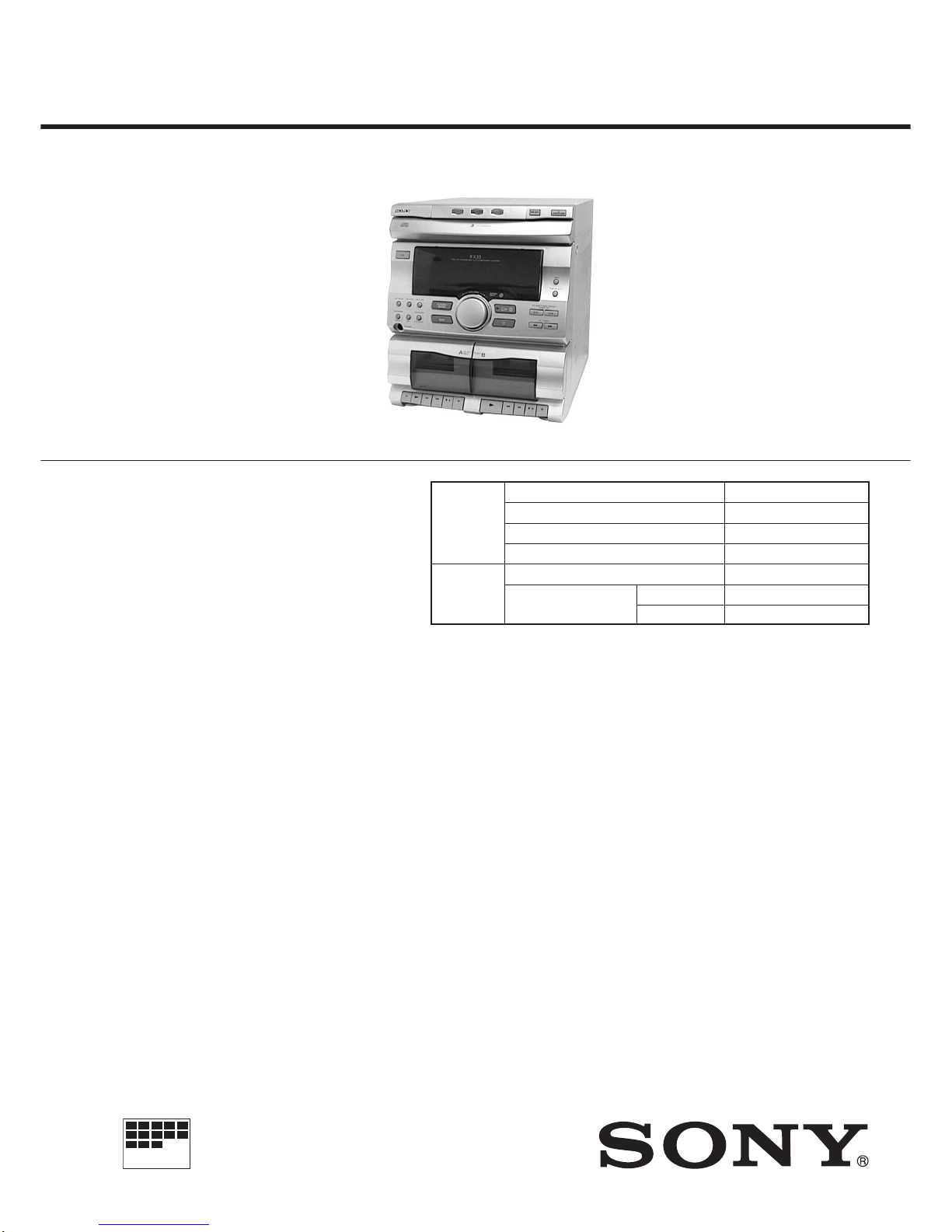
Sony HCD-RX33 User manual

HCD-RX33
AEP Model
UK Model
SERVICE MANUAL
MINI Hi-Fi COMPONENT SYSTEM
MICROFILM
HCD-RX33 is the tuner, deck, CD and
amplifier section in MHC-RX33.
— Continued on next page —
SPECIFICATIONS
Model Name Using Similar Mechanism HCD-G101
CD Mechanism Type CX3
Base Unit Type KSM-213BCM
Optical Pick-up Type KSS-213B/S-N
Model Name Using Similar Mechanism HCD-G101
DECK-A TK20FX-SW943-800
DECK-B TK20FX-SW943-800
CD
SECTION
TAPE
DECK
SECTION Tape Transport
Mechanism Type
The following measured at AC 230 V 50 Hz;
DIN power output (Rated) 25 W + 25 W (6 Ωat 1 kHz, DIN)
Continuous RMS power output (Reference)
35 W + 35W (6 Ωat 1 kHz, 10% THD)
Outputs
PHONES (stereo phone jack) :
accepts headphones of 8 Ωor more
SPEAKER : accepts impedance of 6 to 16 Ω
CD player section
System Compact disc and digital audio system
Laser Semiconductor laser (λ= 780 nm)
Emission duration: continuous
Laser output Max. 44.6 µW*
*This output is the value measured at a distance
of 200 mm from the objective lens surface on the
Optical Pick-up Block with 7 mm aperture.
Frequency response 20 Hz – 20 kHz (± 0.5 dB)
Wavelength 780 – 790 nm
Tape deck section
Recording system 4 -track 2 -channel stereo
Frequency response 60 – 13,000 Hz (± 3dB), using Sony
TYPE Ιcassette
Tuner section
FM stereo, FM/AM superheterodyne tuner
FM tuner section
Tuning range 87.5 – 108.0 MHz
Antenna FM lead antenna
Antenna terminal 75 Ωunbalanced
Intermediate frequency 10.7MHz
AM tuner section
Tuning range 531 – 1,602 kHz
Antenna AM loop antenna
Antenna terminals External antenna terminal
Intermediate frequency 450 kHz

— 2 —
CAUTION
Use of controls or adjustments or performance of procedures
other than those specified herein may result in hazardous
radiation exposure.
Notes on chip component replacement
• Never reuse a disconnected chip component.
• Notice that the minus side of a tantalum capacitor may be
damaged by heat.
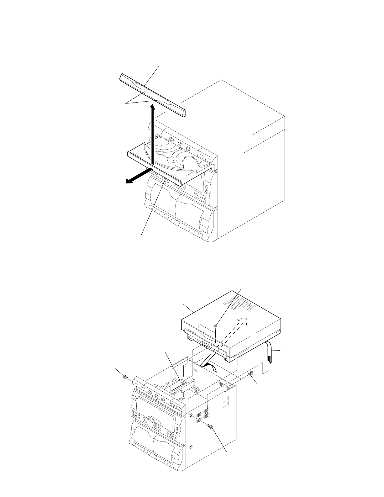
Flexible Circuit Board Repairing
• Keep the temperature of soldering iron around 270˚C
during repairing.
• Do not touch the soldering iron on the same conductor of the
circuit board (within 3 times).
• Be careful not to apply force on the conductor when soldering
or unsoldering.
Laser component in this product is capable of emitting radiation
exceeding the limit for Class 1.
This appliance is classified as
a CLASS 1 LASER product.
The CLASS 1 LASER
PRODUCT MARKING is
located on the rear exterior.
This caution
label is located
inside the unit.
SERVICING NOTE
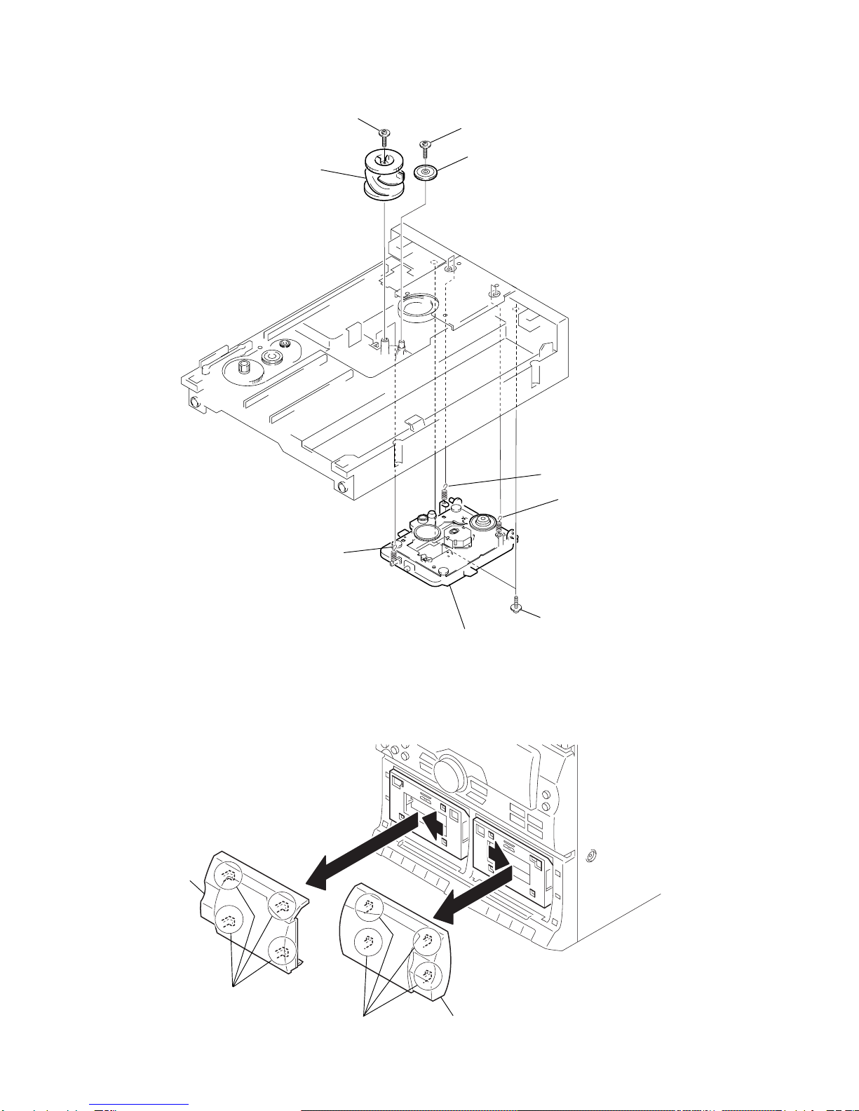
NOTES ON HANDLINGTHE OPTICAL PICK-UP BLOCK
OR BASE UNIT
The laser diode in the optical pick-up block may suffer electrostatic
break-down because of the potential difference generated by the
charged electrostatic load, etc. on clothing and the human body.
During repair, pay attention to electrostatic break-down and also
use the procedure in the printed matter which is included in the
repair parts.
The flexible board is easily damaged and should be handled with
care.
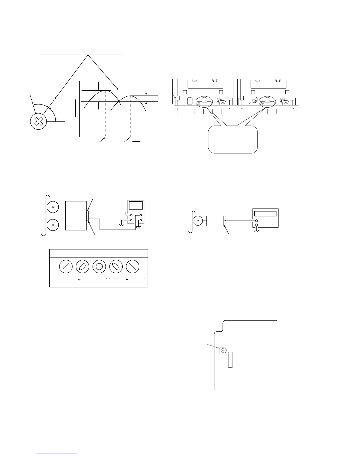
NOTES ON LASER DIODE EMISSION CHECK
The laser beam on this model is concentrated so as to be focused on
the disc reflective surface by the objective lens in the optical pick-
up block. Therefore, when checking the laser diode emission,
observe from more than 30 cm away from the objective lens.
SAFETY-RELATED COMPONENTWARNING!!
COMPONENTS IDENTIFIED BY MARK !OR DOTTED LINEWITH
MARK !ON THE SCHEMATIC DIAGRAMS AND INTHE PARTS
LIST ARE CRITICAL TO SAFE OPERATION. REPLACE THESE
COMPONENTS WITH SONY PARTS WHOSE PART NUMBERS
APPEAR AS SHOWN IN THIS MANUAL OR IN SUPPLEMENTS
PUBLISHED BY SONY.
General
Power requirements 230V AC, 50/60Hz
Power consumption 80 W
Dimensions (w/h/d) incl. projecting parts and controls
Approx. 280 ×320 ×371 mm
(11 1/8×12 5/8×14 5/8in)
Mass Approx. 7.2 kg (15 lb 14 oz.)
Supplied accessories: AM loop antenna (1)
Remote RM-SG5 (1)
FM lead antenna (1)
Design and specifications are subject to change without notice.

— 3 —
TABLE OF CONTENTS
1. GENERAL ..........................................................................4
2. DISASSEMBLY
2-1. CD Door ............................................................................. 5
2-2. CD Mechanism Deck ......................................................... 5
2-3. Front Panel ......................................................................... 6
2-4. Main Board and H.P Board ................................................6
2-5. CD Tray ..............................................................................7
2-6. CD Decoder Board .............................................................7
2-7. Base Unit ............................................................................8
2-8. Cassette Lid (L)/(R)............................................................8
3. MECHANICAL ADJUSTMENTS ............................... 9
4. ELECTRICAL ADJUSTMENTS ................................. 9
5. DIAGRAMS
5-1. Circuit Boards Location ................................................... 14
5-2. Block Diagrams
• Deck Section ................................................................... 15
• Tuner/CD Section ............................................................17
5-3. IC Block Diagrams........................................................... 19
5-4. Schematic Diagram —Main Section —........................... 24
5-5. Printed Wiring Board — Main Section — ....................... 29
5-6. Printed Wiring Board —CD Section — ...........................34
5-7. Schematic Diagram —CD Section —..............................39
5-8. Schematic Diagram — Panel Section — ......................... 43
5-9. Printed Wiring Board —Panel Section — ........................47
5-10. IC Pin Function ................................................................52
6. EXPLODED VIEWS
6-1. Cabinet Section................................................................. 54
6-2. Front Panel Section .......................................................... 55
6-3. Cassette Button Section....................................................56
6-4. Cassette Mechanism Deck Section................................... 57
6-5. CD Mechanism Deck Section 1 ....................................... 58
6-6. CD Mechanism Deck Section 2 ....................................... 59
6-7. Base Unit Section (KSM-213BCM)................................. 60
7. ELECTRICAL PARTS LIST ........................................ 61

— 4 —
SECTION 1
GENERAL
LOCATION OF PARTS AND CONTROLS
1Disc tray
2DISC 1 button
3DISC 2 button
4DISC 3 button
5DISC SKIP button
6§OPEN/CLOSE button
7DBFB button
8VOLUME knob
9Display window
!º CLOCK TIMER SET button
!¡ TIMER ON/OFF button
!™ DISPLAY DEMO
!£ TUNER/BAND
!¢ ·∏(play/pause) button
!∞ ENTER/NEXT button
!§ ≠±CD AMS/TUNER PRESET TIMER
SET buttons
!¶ FILE SELECT
!• I/u(POWER) button
!ª TUNER MEMORY REPEAT button
@º EDIT button
@¡ STEREO/M NO, PLAY MODE button
@™ TAPE button
@£ π(STOP) button
@¢ 0)CD/TUNER button
@∞ PHONES jack
@§ Deck A, PLAY/REC
@¶ Deck B, PLAY
@• Tape operaying buttons
r(recording)
((play)
0(fast rewind)
)(fast forward)
p6(stop/eject)
P(pause)
7
!¶
123456
9
!§
!∞
!¢8!£!™
!¡
!•
!º
!ª @º @¡ @™ @£ @¢
@∞
@§
@•
@¶

— 5 —
SECTION 2
DISASSEMBLY
Two claws
1
Pull out the CD tray and remove the CD door
with releasing claws into the direction of arrow.
2
CD door
2-1. CD DOOR
Note : Follow the disassembly procedure in the numerical order given.
6
CD mechanism deck
1
Two screws (+B 3
×
8)
3
Two screws (+BVTP 3
×
10)
2
Screw (+PTPWH 3
×
10)
2
Screw (+PTPWH 3
×
10)
4
Flat type wire (CN09)
5
Harness (CN302)
2-2. CD MECHANISM DECK

— 6 —
7
Screw
(+PTPWH 3
×
10)
3
Screw (+BVTP 3
×
10)
4
Screw (+BVTP 3
×
10)
5
Two screws (+BVTP 3
×
10)
6
Two screws
(+BVTP 3
×
10)
7
Screw (+PTPWH 3
×
10)
8
Screw (+BVTP 3
×
10)
2
Three screws
(+BVTP 3
×
10)
1
Connector (CN401)
9
Front panel
HOW TO SET THE
POWER CORD
power cord
1
Harness (CN303)
8
H.P board
2
Harness (CN204)
3
Connector
4
Connector (CN202)
5
Connector (CN201)
7
MAIN board
6
Two screws
(+KTP 3
×
8)
Craw
2-3. FRONT PANEL
2-4. MAIN BOARD AND H.P BOARD

— 7 —
1
Screw
(+P 2.6
×
4)
2
Bracket
4
Bracket
5
Flat type wire
(CN06)
3
Screw
(+P 2.6
×
4
)
6
CD tray
1
Two screws (+BVTP 3
×
10)
2
Two screws (+BVTP 3
×
10)
Two claws
7
CD DECODER board
3
Belt
6
Flat type wire (CN06)
5
Flat type wire (CN01)
4
Connector (CN05)
!º
Connector (CN03)
8
Two screw
(+BVTP 3
×
10)
9
Sheet
Claw
Claw
2-5. CDTRAY
2-6. CD DECODER BOARD

— 8 —
2
Screw
(+PTPWH 2.6
×
8)
3
UD-gear
4
Screw
(+PTPWH 2.6
×
8)
5
UD-Cam
8
Spring
7
Spring
6
Spring
1
Two screws
(+KTP 3
×
8
)
9
Base unit
Four claws
Four claws
2
Cassette lid (R)
1
Cassette lid (L)
2-7. BASE UNIT
2-8. CASSETTE LID (L) / (R)

— 9 —
Precaution
1. Clean the following parts with a denatured alcohol-moistened
swab:
record/playback head pinch rollers
erase head rubber belts
capstan idlers
2. Demagnetize the record/playback head with a head
demagnetizer.
3. Do not use a magnetized screwdriver for the adjustments.
4. After the adjustments, apply suitable locking compound to the
parts adjusted.
5. The adjustments should be performed with the rated power
supply voltage unless otherwise noted.
Torque Measurement
SECTION 3
MECHANICAL ADJUSTMENTS
Meter reading
40 to 70 g • cm
(0.56 - 0.97 oz • inch)
1 to 5 g • cm
(0.01 - 0.07 oz • inch)
55 to 140 g • cm
(0.76 - 1.94 oz • inch)
Torque
FWD
FWD
back tension
FF/REW
Torque meter
CQ-102C
CQ-102C
CQ-201B
SECTION 4
ELECTRICAL ADJUSTMENTS
1. Demagnetize the record/playback head with a head
damagnetizer.
2. Do not use a magnetized screwdriver for the adjustments.
3. After the adjustments, apply suitable locking compound to the
parts adjusted.
4. The adjustments should be performed with the rated power
supply voltage unless otherwise noted.
5. The adjustments should be performed in the order given in this
service manual. (As a general rule, playback circuit adjustment
should be completed before performing recording circuit
adjustment.)
6. The adjustments should be performed for both L-CH and R-
CH.
Record/Playback Head Azimuth Adjustment
(Deck A, Deck B)
Note: Perform this adjustments for both decks.
Procedure:
1. Mode : Playback
DECK SECTION 0 dB=0.775V
Tape
P-4-A100
WS-48B
Signal
10 kHz, –10 dB
3 kHz, 0 dB
Used for
AzimuthAdjustment
Tape Speed Adjustment
test tape
P-4-A100
(10kHz, –10dB) SPEAKER
terminal (JK501)
level meter
+
–
set

— 10 —
2. Turn the adjustment screw and check output peaks. If the peaks
do not match for L-CH and R-CH, turn the adjustment screw
so that outputs match within 2 dB of peak.
3. Mode: Playback
4. After the adjustments, apply suitable locking compound to the
parts adjusted.
Adjustment Location:
Remove the cassette lid before adjustment (See page 8)
test tape
WS-48B
(3kHz, 0dB)
Tape Speed Adjustment (Deck A)
Procedure:
1. Mode: Playback
2. Adjust the SFR201 so that the frequency counter reads 3,000
Hz ± 90Hz.
Adjustment Location: MAIN board
Sample Value of Wow and flutter
W. RMS (JIS) within 0.3%
(test tape: WS-48B)
[MAIN BOARD] — Component side —
CN204
L-CH
peak
R-CH
peak
screw
position
output
level within
2dB within 2dB
L-CH
peak
screw
position
R-CH
peak
test tape
P-4-A100
(10kHz, –10dB) SPEAKER
terminal (JK501)
(L-CH)
set
L
R
oscilloscope
SPEAKER
terminal (JK501)
(R-CH)
Waveform of oscilloscope
in phase 45˚ 90˚ 135˚ 180˚
good wrong
SPEAKER
terminal (JK501)
set
frequency counter
+
–
SFR201
Tape Speed
Adjustment screws
REC/PB head (deck A)
or PB head (deck B)

— 11 —
TUNER SECTION 0 dB=1µV
AM Tuning Voltage Adjustment
Procedure:
1. Set the reception frequency of the unit to 531 kHz.
2. Adjust L108 for 1.2 ± 0.05 V reading on the DC voltmeter.
3. Set the reception frequency of the unit to 1,602 kHz.
4. Confirm that the voltage reading on the DC voltmeter is within
8.0 ± 0.5 V.
Adjustment Location: MAIN board (See page 12)
AMTracking Adjustment
Procedure:
1. Tune the set to 600 kHz.
2. Set the output ofAM RF SSG so that the input level of the set
will become 60 dB (µV/m).
3. Adjust L107 so that when the waveform on the oscilloscope is
maximum, no noise appears.
4. Tune the set to 1,400 kHz.
5. Adjust TC101 so that when the waveform on the oscilloscope
is maximum, no noise appears.
• Repeat the procedures in each adjustment several times, and the
tracking adjustment should be finally done by the trimmer
capacitors.
Adjustment Location: MAIN board (See page 12)
TP1
+
DC voltmeter
Main board
–
F
G
VT
AM RF SSG
loop antenna
set
loop antenna
(Supplied accessories)
60 cm AM ANTENNA
terminal (TM1)
30% amplitude
modulation by
400 Hz signal Field strength dB (
µ
V/m) =SSG output level dB (
µ
V/m) –26 dB.

— 12 —
FMTuned Level Adjustment
set
Procedure:
1. Supply a 28 dB 98 MHz signal from theANTENNA terminal.
2. Tune the set to 98 MHz.
3. Adjust SFR101 to the point (moment) when the TUNED
indicator will change from going off to going on.
Adjustment Location: MAIN board
Adjustment Location
[MAIN BOARD] — Component side —
JK501
JK101
L108
TC101
L107
SFR101
IC102
TP1
IC103
AM
Trackin
g
AM Tuning
Voltage
FM Tuned Level
FM RF SSG
Carrier frequency : 98 MHz
Modulation : AUDIO 1 kHz, 75 kHz
deviation (100%)
Output level : 28 dB (at 75
Ω
open)
FM ANTENNA terminal
(JK101)
75
Ω
coaxial

— 13 —
IC03 VR02
VR01
R07
IC01
CN12
Focus Gain
Focus Bias
RF Level
CD SECTION
Note:
1. CD Block is basically constructed to operate without
adjustment. Therefore, check each item in order given.
2. UseYEDS-18 disc (3-702-101-01) unless otherwise indicated.
3. Use an oscilloscope with more than 10MΩimpedance.
4. Clean the object lens by an applicator with neutral detergent
when the signal level is low than specified value with the
following checks.
5. Adjust the focus biasadjustmentwhen optical block isreplaced.
Focus Bias Adjustment
RF Level Check
Procedure :
1. Connect oscilloscope to test pointTP (RF) on CD DECODER
board.
2. Turned Power switch on.
3. Put disc (YEDS-18) in and playback.
4. Confirm that oscilloscope waveform is clear and check RF
signal level is correct or not.
Note: Clear RF signal waveform means that the shape “◊” can be
clearly distinguished at the center of the waveform.
oscilloscope
level: 1.0 Vp-p
VOLT/DIV: 200 mV
TIME/DIV: 500 nS
+0.3
–0.2
Adjustment Location: CD DECODER board
Procedure:
1. Connect DC voltmeter to test point CN12 (FEO), (VC) on CD
DECODER board.
2. Turned Power switch on.
3. Put disc (YEDS-18) in and stop.
4. Adjust VR01 so that the DC voitmeter reading is 0 ± 20 mV.
Adjustment Location: CD DECODER board
Focus Gain Adjustment (VR02)
This gain has a margin, so even if it is slightly off.
There is no problem.
Therfore, do not perform this adjusment.
Please note that it should be fixed to mechanical center position
when you moved and do not know original position.
Adjustment Location
[CD DECODER BOARD] — Component side —
CD DECODER
boardCN12
FEO
VC
DC voltmeter
+
–
CD DECODER
board
TP (RF)
CN12 (VC)

— 14 —
SECTION 5
DIAGRAMS
5-1. CIRCUIT BOARDS LOCATION
SW (C) board
SW (D) board SW (B) board
DISK board
PANEL board
CD DECODER board
H.P board
SENSOR board
R/P SWITCH board
VR board
AC POWER boar
d
MAIN board
SW (A) board
MOTOR board
MOTOR (6P) (S) board

HCD-RX33
5-2. BLOCK DIAGRAMS
— DECK SECTION —
— 15 — — 16 —
HP901
PB
HEAD
TAPE B
HRP901
REC/PB
HEAD
TAPE A
R CHR CH
R CH
PLAY/REC
CONTROL
Q203, 205
PLAY/REC
CONTROL
DRIVE
Q207
MUTE
SWITCH
Q216
TAPE A/B
SWITCH
Q213
PLAY/REC
CONTROL
D209
L201
BIAS OSC
BIAS
OSC
Q218
HE901
ERASE
HEAD
R CH
1
2
9
3
REC OUT
PB OUT
A/B
5
19
11
10
REC/PB
EQ AMP
IC201
TAPE A/B
Q209
MUTE
TAPE A
SWITCH
Q214
Q211
Q220
REC SWITCH
MUTE
CONTROL
Q
Q217
D205 D203
D202
D212
D210
D211
D210
S201
A DECK
S202
B DECK
S203
PLAY
M
D207D206
M901
REC/CAPSTAN
MOTOR
TAPE SPEED
SFR201
+11.5V
D208
SW201
REC/PLAY
PLAY
REC
: FM
: CD
• Signal Path
• RCH is omitted
B
CD
SECTION
TU L
11
9
Q301
10
ST IND
TU MUTE
DO
CD L
12
CONTROL
3 2 1
CLK
14
DI
15
CE
13
SELECTOR
IC301
CLK
DI
CE
LINE AMP
IC302
7
5
BASS BOOST
SWITCH
Q307 Q303
MUTE
13 2
7 4
POWER AMP
IC501
SPEAKER
RELAY
DRIVE
Q551
Q553 1
26
IC502IC502
RL501
R CH
SPEAKER
PHONES
JK501
JK303
SCOR
SENS
SQSO
XLAT
SQCK
DATA
DI
CLK
CE
STB
26
STB
21
CE
22
CLK
23
DI
18
DATA
17
SQCK
20
XLAT
19
SQSO
51
SENS
38
SCOR
MUTE
DRIVE
Q583,584
Q604
MUTE
MUTE
SWITCH
Q603
CD SYNC
SWITCH
Q208
4
TU MUTE
24
DI1
48
SYS REC
7
DBFB
3
SYSTEM MUTE
2
POWER
LED DRIVE
IC602
2
3
4
36
ALATCH
11
13 LED
DRIVE
DI
CLK
Q208
Q605,606
RESET
SWITCH POWER
DOWN DET
Q601
10
RESET
15
POWER DOWN
Q602
LED602
LED601
Q602
D602
X2
11
X1
12
VR UP
44
X601
4.19MHz
VR DOWN
45
VR601
ENCODER
PIC UP
55
PIC DOWN
56
TRAY OPEN
59
TRAY CLOSE
60
TURN TABLE
58
DISC COUNT
57
AB
S02
TRAY
OPEN/CLOSE
DET
S03
DISC
COUNTER
DET
S04
TURNTABLE
OPERATION
DET
S01
CD DECK
UP/DOWN
DET
3
2
Q601 RM601
REMOTE
CONTROL
RECEIVER
39
REMOTE
64 78
KEY
MATRIX
S601-623
P1 P21 100 86
G1 G15
.81 85
33 29
KI0 KI4
FLD601
FLD DISPLAY
SYSTEM CONTROLLER/
FLD DRIVER
IC601
+5.6V
REG
Q404
SITCHING
Q406,407
+11.5V
(SWITCHED)
+11.5V FILTER
Q402
+7.9V
REG
Q403
+7.9V +12V
REG
Q401
RECT
D405-408
MUTE
Q585,586
P MUTE
CONT
Q409
AC OFF
DET
Q410
D417
D416
D553
RECT
D401
D409
-12V
-30V
+30V
-27V
REG
Q408
-27V VOLTAGE
DOUBLER
D414,415
AC
IN
PT001
AC3.4V
AC3.4V
12
16
A
TUNER
SECTION
: PB (DECK A)
: PB (DECK B)
: REC (DECK A)
Q207
Q201
CE
CLK
DI
COUNT
FOK
52
FOK
53
COUNT
47
FM ST IND

HCD-RX33
—TUNER/CD SECTION —
— 17 — — 18 —
CE
19 12
5
3
4
2
24
1
PLL
IC102
FM
XO
XI CLK
DI
DO
CE
CLK
DI
DO
OPTICAL PICK-UP
BLOCK
APC
Q01 38
+5V
VC
LD
GND
A
C
B
E
F
FOCUS
COIL
F+
F
T+
T
TRACKING
COIL
33
34
39
36
35
48
APC
FOCUS PHASE
COMPENSATION
DECODER
SERIAL/
PARALLEL
CONVERTER
FE
AMP
RF
AMP
IIL
TTL
TTL
IIL
COMAND
VC
TRACKING PHASE
COMPENSATION
LD
PD
E
F
PD1
PD2
6
24
23
20
19
22
21
31
25
SENS
RFO
FOK
C OUT
DATA
XLT
CLK
XRST
13
FEO TAO
IC03
T.T/TRAY MOTOR
DRIVER
CD RF/SERVO
PROSSESOR
IC01 (1/2)
4
5
T IN
3
2
1
VR
PD
PD
18
17
20
19
6
F IN
22
SL IN
13
T.T F IN
F+
F
T+
T
SL+
SL
SP+
SP
M
M
MOTOR
M102
SLED
MOTOR
M101
SPINDOL
EFM
DEMO.
XRST
CLV
SERVO
DIGITAL
CLV
D/A
I/F
SUB CODE
PROSSESOR
CPU I/F
911 5 4 7 61
MDP
SENS
SCOR
SQSO
SQCK
CLOCK
DATA
CLK
XLT
DAT
SE
CN
FOK
RF
SERIAL
I/F PWM
PWM 70
69
73
74
NL
L
XTA1
XTA0 X701
MUTE
R-CH
CD DIGITAL
SIGNAL PROCESSOR
IC04
16
:FM
:CD
• SIGNAL PATH
14
7
8
4
2
1
6
10
DETECTOR
16
OSC
FM
75Ω
AM
ANTENNA
JK101
8RF MIX 1
3
FM FRONT END
FE101
RF IF
AMP
Q101
CF101
10.7MHz CF102
10.7MHz
L105
MW OSC
IF
G
VT
AM/FM
TUNING
VOLTAGE
TP1
L107
AM ANT
AM RF
AMP
Q103
MPX
16
FM IF
1
OSC
23
AFC
22 AM RF
21
FM
IF
AF DET
18
FM
DET
AM/FM
IF BUFF
AM
OSC AM
MIX
AM
DET
SMET
20
CF103
450kHz
MUTE
AGC
AM
IF
DECODER 14
L
15
R
4
2
T102
AM IFT
8
FM DET
17
MPX VCO
CF104
10.7MHz
CF105
19kHz
R CH
FM/AM MPX
IC101
L.P.F
Q104,105
FM
TUNED
LEVEL
PD1
21
X201
7.2MHz
FM B+
17
TUB+
B+
Q105
PL DET
13
18
AM
OSC/FMSD
24
B+
7
SD
PH DET
11
PH DET
12
14
ST/MONO
TU LED
6
13
AM/FM
SD
15
L CTR 16
R CTR
7
ST IND
10
AM/FM
MUTE
Q107
TU L
ST IND
TU MUTE
DO
A
MAIN
SECTION
D
5
LD ON
SWITCH
Q02
LD
PD
F/T COIL
SL/SP MOTOR
CN12
CN2
ATSC
45 FEO
1
TEO
42
FOCUS
TRACKING
37 40
FE BIAS EI
RV01
FOCUS
GAIN
RV02
14
15
30
31
T.T+
T.T
TR+
TR
M
M
MOTOR
T/T
MOTOR
TRAY
21
SP IN
29
TR F IN
12
T.T R IN
28
TR T IN
27
MUTE IN
IC06
IC01 (2/2)
67
REG
Q11
9
REG I
10
REG B
11
REG OUT
7
VCC 8
VCC
+5V
+7.5V
XRST
6
SPEED
11
CONTRL
5
SWITCH
Q04
13
14
TR+
TR
7
14
T.T+
T.T
4
MUTE
2
DATA 3
CLOK
1
STB
IC02
MOTOR DRIVE
REG CONTROL
T.T/TRAY
36
23
14
13
15
16
17
8
25
18
SPOA
LIMIT
SWITCH
S05
10
XLAT
CLOCK
GEN.
PWM
PWM 77
78
NR
R
22
XLON
1
3
2IC05
MIX AMP
MUTE
Q311
CD L
SCOR
SENS
SQSO
XLAT
SQCK
DATA
CE
STB
CLK
DI
B
MAIN
SECTION
:AM
• RCH is omitted
SFR101
CLK
DI
COUNT
FOK

— 19 —
DRIVER
DRIVER
GND
MUTE
CONTROL
XRST
T.T(M)
POSI.1
POSI.2
T.T.SW
VDD
STB
CLOK
DATA I
DATA 0
LOADING
M-
LOADING
M+
SENSOR
1
8
2
3
4
5
6
7
16
9
15
T
C14
13
12
11
10
SERIAL I/O
CONTROL
LATCH
LATCHLATCH
IC02 (CD DECORD BOARD)TC9173P
5-3. IC BLOCK DIAGRAMS
+–
LEVEL SHIFT
+–
+–
1 2 345678910 11 12 13 14
28 27
LEVEL SHIFT
+–
+
–
MUTE
+
–
+–
LEVEL SHIFT
+–
+–
LEVEL SHIFT
+–
+
–
+
–
15
1617
18
19
21 20
22
26 25 24 23
+–
NC
Vcc
VccVcc
VCC
BIAS IN
IN1B
IN1A
IN2B
IN2A
GND
GND
MUTE
VCC
OUT2A
OUT2B
OUT1A
OUT1B
IN4B
IN4A
IN3B
IN3A
OP OUT
OP IN (–)
OP IN (+)
GND
NC
VCC
OUT3A
OUT3B
OUT4A
OUT4B
IC03 (CD DECORD BOARD) BA5941FP

— 20 —
36
PHD2
PHD1
PHD
33
LD
32
RF M
31
RF O
30
RF I
29
CP
28
CB
27
CC1
26
CC2
25
FOK
24 SENS
23 C. OUT
22 XRST
21 DATA
20 XLT
19 CLK
18 VCC
17 ISET
16 SL 0
15 SL M
14 SL P
13
12
TA O
TA M
11
FSET
10
TG2
9
TGU
8
SRCH
7
FE M
6
FE O
5
FLB
4
FGD
3
FDFCT
2
FEI
1
FEO
48VC
47TDFCT
46TZC
45ATSC
44TEI
43LPFI
42TEO
41VEE
40EI
39E
38F
37FE BIAS
+
+
–
+
+
–
+
–
+
–
+
–
+
–
+
–
+
+
+
–
+
–
+
–
+
–
+
–
+
–
+
–
+
–
–
+
+
–
–
+
+
–
+
–
+
–
+
–
+
–
APC
–
–
–
–
LEVELS
FOK
MIRR
DFCT
RF IV AMP2
RF IV AMP1
FE AMP
F IV AMP
E IV AMP
TE AMP
FZC COMP
BAL1
BAL2
BAL3
TOG1
TOG2
TOG3
TTL
IIL
IIL
TTL
TTL
IIL
• IIL DATA RESISTOR • INPUT SHIFT RESISTOR
• ADDRESS DECODER
• OUTPUT DECODER
HPF COMP LPF COMP
TZC COMP
DFCT
DFCT
TM1
FS4
ATSC
• WINDOW COMP
• FCS PHASE
COMPENSATION
• TRACKING
• PHASE
COMPENSATION
• ISET
FS1
FS2
TM4
TM5
TM6
TM3
TM7
TG2
• F SET
TG1
TM2
+
–
TOG1-3 FS1-4 TG1-2 TM1-7 PS1-4
BAL1-3
35 34
IC01 (CD DECORD BOARD) CXA1782BQ

— 21 —
FM IF REG GND VCC
FM DET
S-CURVE TUNING
DRIVE
LEVEL
DET
AM/FM
IF BUFE
ALC
BUFFER
AM
OSC AM
MIX
AM
RF AMP
AGC
AM DETAM IF
COMP
FM
AM
MUTE DECORDER
STEREO DRIVE
FF
TRIG
PHASE
DET
VCO
AM/FM
SW
PILOT
DET
STEREO SW
36 9 122 5 8 11
14 7 10
22 19 16 13
23 20 17 14
24 21 18 15
OSC/FMSD OSC AFC AM RF SMET AM HPF AF DET MPX VCO MPX IN R OUT L OUT PL DET
FM IF AM MIX REG AM IF GND TU LED ST IND FM DET VCC AM/FM PH DET PH DET
XIN
CE
DI
CL
DO
SYC
IN0
IN1
OUT0
OUT1
OUT2
OUT3
SHIFT REGISTER
LATCH
12 BIT
PROGRAMMABLEDIVIDER
SWALLOW COUNTER
1/16 . 1/17 BIT
REFERENCE
DIVIDER PHASE DETECTOR
CHARGE PUMP
1 / 2
X OUT
VSS
PD2
PD1
VDD
FM IN
AM IN
OUT 6
HCTR
LCTR
OUT 5
OUT 4
UNIVERSAL
COUNTER
7
10
11
12
9
8
6
5
4
3
2
1
13
14
24
23
22
21
20
19
18
17
16
15
IC102 (MAIN BOARD) LA1831
IC103 (MAIN BOARD) LC7218-ST

— 22 —
+
–
3
6
9
12
15
2
5
8
11
14
1
4
7
10
13
28
25
22
19
16
29
26
23
20
17
30
27
24
21
18
+
–
+
–
+
–
LATCH
DECODER
CONTROL
SHIFT
REGISTER
–
+
LVROUT
LVRIN
LTOUT
LTCOM
LT4
LT3
LT2
LT1
L4
L3
L2
L1
VDD
CL
DI
RVROUT
RVRIN
RTOUT
RTCOM
RT4
RT3
RT2
RT1
R4
R3
R2
R1
VREF
VSS
CE
CH2/A CH2/B NF VCC CG NF ALC
METAL
OUT PRE
OUT TAPE A
/TAPE B REC
OUT REC
IN
CH1/A CH1/B NF GND1 M/H NF
CH2 CH2
ALC
M/N
CH1
GNDGND
CH1
+
–+
–
+
–+
–
A/B
GNDMETAL
OUT PRE
OUT MIX
OUT REC
OUT REC
IN
IREF VREF2
VREF1
24 23 22 21 20 19 18 17 16 15 14 13
123456789101112
IC301 (MAIN BOARD) LC75392
IC201 (MAIN BOARD)TA8189N
Table of contents
Other Sony Stereo System manuals

Sony
Sony MHC-G100 User manual

Sony
Sony HCD-VZ0 User manual

Sony
Sony CMT-CP100K User manual

Sony
Sony ZS-BTG905 User manual

Sony
Sony CMT-GS30DAB User manual

Sony
Sony HCD-BX6AV User manual

Sony
Sony LBT-SH2000 User manual

Sony
Sony HCD-ZX66I - Cd/receiver Component For Compact Hi-fi Stereo... User manual

Sony
Sony WX-GT90BT User manual

Sony
Sony WHG-SLK1i - Audio System Component User manual