Sony MHC-EC619iP User manual

SERVICE MANUAL
Sony Corporation
Published by Sony Techno Create Corporation
HOME AUDIO SYSTEM
9-893-792-01
2013H33-1
© 2013.08
US Model
MHC-EC619iP/EC719iP
Canadian Model
AEP Model
UK Model
E Model
MHC-EC619iP
Australian Model
MHC-EC619iP/EC719iP/EC919iP
Ver. 1.0 2013.08
4-467-785-11 MANUAL, INSTRUCTION (ENGLISH)
(EC619iP: US, CND, UK, E2, AUS)
4-467-785-21 MANUAL, INSTRUCTION (FRENCH)
(EC619iP: CND, AEP, E2)
4-467-785-31 MANUAL, INSTRUCTION (SPANISH)
(EC619iP: US, AEP, E2)
4-467-785-41 MANUAL, INSTRUCTION (GERMAN)
(EC619iP: AEP)
4-467-785-51 MANUAL, INSTRUCTION (DUTCH)
(EC619iP: AEP)
4-467-785-61 MANUAL, INSTRUCTION (ITALIAN)
(EC619iP: AEP)
4-467-785-71 MANUAL, INSTRUCTION (POLISH)
(EC619iP: AEP)
4-467-786-11 MANUAL, INSTRUCTION (ENGLISH)
(EC719iP/EC919iP)
4-467-786-31 MANUAL, INSTRUCTION (SPANISH)
(EC719iP: US)
• The service policy of these models are Product Exchange.
The following parts are available for service parts of these models.
PARTS LIST
Ref. No. Part No. Description Remark
MHC-EC619iP/EC719iP/EC919iP
HCD-EC619iP/EC719iP/EC919iP/SS-EC719iP/ECL5/WG919iP
• MHC-EC619iP/EC719iP/EC919iP are composed of following models.
MHC-EC619iP MHC-EC719iP MHC-EC919iP
Compact Disc Receiver HCD-EC619iP HCD-EC719iP HCD-EC919iP
Front Speaker SS-ECL5 SS-EC719iP SS-EC719iP
Subwoofer – – SS-WG919iP
• Abbreviation
AUS : Australian model
CND : Canadian model
E2 : 120V AC area in E model
Note 1: The speaker (SS-ECL5) supplied with MHC-EC619iP has a different service policy
from the speaker (SS-ECL5) supplied with other models. For SS-ECL5 supplied with
models other than MHC-EC619iP, refer to the separate SS-ECL5 service manual.
Be sure to check the system model name before beginning service.
Note 2: The speaker (SS-EC719iP) supplied with MHC-EC719iP (US and Australian models)
and the speakers (SS-EC719iP/WG919iP) supplied with MHC-EC919iP (Australian
model) have different service policies from speakers (SS-EC719iP/WG919iP) sup-
plied with different models (or intended for different regions).
For SS-EC719iP or SS-WG919iP supplied with models other than MHC-EC719iP (US
and Australian models) and MHC-EC919iP (Australian model), refer to the separate
SS-EC719iP/WG919iP service manual.
Be sure to check the system model name before beginning service.
1 A-1970-520-A REMOTE COMMANDER (RM-AMU185)
(Remote control) (EC619iP)
1 A-1970-521-A REMOTE COMMANDER (RM-AMU186)
(Remote control) (EC719iP/EC919iP)
2 4-486-327-01 SPEAKER PAD (PORON T2) (Speaker pads)
(4 pieces, 1 sheet) (EC619iP)
2 4-486-328-01 SPEAKER PAD (SILICON T4) (Speaker pads)
(4 pieces, 1 sheet) (EC719iP/EC919iP)
3 9-885-189-78 AM ANTENNA (AM loop antenna)
(EC719iP/EC919iP)
4 9-885-189-79 FM ANTENNA (FM lead antenna)
Ref. No. Part No. Description Remark
1
RM-AMU185
2
Speaker pads
3
AM loop antenna
(MHC-EC719iP/EC919iP)
4
FM lead antenna
1
RM-AMU186

MHC-EC619iP/EC719iP/EC919iP
REVISION HISTORY
Ver. Date Description of Revision
1.0 2013.08 New

SERVICE MANUAL
Sony Corporation
Published by Sony Techno Create Corporation
HCD-EC719iP/EC919iP
SPECIFICATIONS
COMPACT DISC RECEIVER
9-893-801-01
2013H33-1
© 2013.08
US Model
Canadian Model
HCD-EC919iP
AEP Model
UK Model
HCD-EC719iP
Ver. 1.0 2013.08
• HCD-EC719iP is compact disc receiver in MHC-EC719iP.
• HCD-EC919iP is compact disc receiver in MHC-EC919iP.
Model Name Using Similar Mechanism NEW
Mechanism Type TDL-5
Photo: HCD-EC919iP

HCD-EC719iP/EC919iP
2
SAFETY-RELATED COMPONENT WARNING!
COMPONENTS IDENTIFIED BY MARK 0OR DOTTED LINE
WITH MARK 0ON THE SCHEMATIC DIAGRAMS AND IN
THE PARTS LIST ARE CRITICAL TO SAFE OPERATION.
REPLACE THESE COMPONENTS WITH SONY PARTS
WHOSE PART NUMBERS APPEAR AS SHOWN IN THIS
MANUAL OR IN SUPPLEMENTS PUBLISHED BY SONY.
CAUTION
Use of controls or adjustments or performance of procedures
other than those specified herein may result in hazardous radia-
tion exposure.
SAFETY CHECK-OUT
After correcting the original service problem, perform the follow-
ing safety check before releasing the set to the customer:
Check the antenna terminals, metal trim, “metallized” knobs,
screws, and all other exposed metal parts for AC leakage.
Check leakage as described below.
LEAKAGE TEST
The AC leakage from any exposed metal part to earth ground and
from all exposed metal parts to any exposed metal part having a
return to chassis, must not exceed 0.5 mA (500 microamperes.).
Leakage current can be measured by any one of three methods.
1. A commercial leakage tester, such as the Simpson 229 or RCA
WT-540A. Follow the manufacturers’ instructions to use these
instruments.
2. A battery-operated AC milliammeter. The Data Precision 245
digital multimeter is suitable for this job.
3. Measuring the voltage drop across a resistor by means of a
VOM or battery-operated AC voltmeter. The “limit” indication
is 0.75 V, so analog meters must have an accurate low-voltage
scale. The Simpson 250 and Sanwa SH-63Trd are examples
of a passive VOM that is suitable. Nearly all battery operated
digital multimeters that have a 2 V AC range are suitable. (See
Fig. A)
1.5 kΩ0.15 μF
AC
voltmeter
(0.75 V)
To Exposed Metal
Parts on Set
Earth Ground
Fig. A. Using an AC voltmeter to check AC leakage.
ATTENTION AU COMPOSANT AYANT RAPPORT
À LA SÉCURITÉ!
LES COMPOSANTS IDENTIFIÉS PAR UNE MARQUE 0SUR
LES DIAGRAMMES SCHÉMATIQUES ET LA LISTE DES
PIÈCES SONT CRITIQUES POUR LA SÉCURITÉ DE FONC-
TIONNEMENT. NE REMPLACER CES COMPOSANTS QUE
PAR DES PIÈCES SONY DONT LES NUMÉROS SONT DON-
NÉS DANS CE MANUEL OU DANS LES SUPPLÉMENTS
PUBLIÉS PAR SONY.

HCD-EC719iP/EC919iP
3
1. SERVICING NOTES ............................................. 4
2. DISASSEMBLY
2-1. Disassembly Flow........................................................... 7
2-2. Side Cover, Top Cover Block ......................................... 8
2-3. Power Cord (AC1), Rear Panel Block ............................ 9
2-4. CD Door.......................................................................... 10
2-5. Front Panel Block ........................................................... 10
2-6. MAIN Board Block ........................................................ 11
2-7. MAIN Board ................................................................... 11
2-8. POWER Board................................................................ 12
2-9. FRONT Board................................................................. 13
2-10. USB Board...................................................................... 14
2-11. Loader with FFC (TDL-5) (CDM1) ............................... 14
3. TEST MODE ............................................................ 15
4. ELECTRICAL CHECK ......................................... 15
5. DIAGRAMS
5-1. Block Diagram ................................................................ 16
5-2. Printed Wiring Board - MAIN Board - ........................... 18
5-3. Schematic Diagram - MAIN Board (1/7) - ..................... 19
TABLE OF CONTENTS
5-4. Schematic Diagram - MAIN Board (2/7) - ..................... 20
5-5. Schematic Diagram - MAIN Board (3/7) - ..................... 21
5-6. Schematic Diagram - MAIN Board (4/7) - ..................... 22
5-7. Schematic Diagram - MAIN Board (5/7) - ..................... 23
5-8. Schematic Diagram - MAIN Board (6/7) - ..................... 24
5-9. Schematic Diagram - MAIN Board (7/7) - ..................... 25
5-10. Printed Wiring Board - FRONT Board -......................... 26
5-11. Schematic Diagram - FRONT Board - ........................... 27
5-12. Printed Wiring Board - POWER Board -........................ 28
5-13. Schematic Diagram - POWER Board - .......................... 29
5-14. Schematic Diagram
- USB/TUNER/DOCKING Boards -.............................. 30
5-15. Printed Wiring Boards
- USB/TUNER/DOCKING Boards -.............................. 31
6. EXPLODED VIEWS
6-1. Cover Section.................................................................. 32
6-2. Rear Panel Section .......................................................... 33
6-3. Front Panel Section ......................................................... 34
6-4. Main Section ................................................................... 35
7. ELECTRICAL PARTS LIST .............................. 36

HCD-EC719iP/EC919iP
4
SECTION 1
SERVICING NOTES
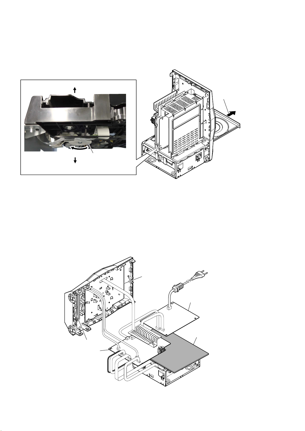
NOTES ON HANDLING THE OPTICAL PICK-UP
BLOCK OR BASE UNIT
The laser diode in the optical pick-up block may suffer electro-
static break-down because of the potential difference generated by
the charged electrostatic load, etc. on clothing and the human body.
During repair, pay attention to electrostatic break-down and also
use the procedure in the printed matter which is included in the
repair parts.
The flexible board is easily damaged and should be handled with
care.
NOTES ON LASER DIODE EMISSION CHECK
The laser beam on this model is concentrated so as to be focused
on the disc reflective surface by the objective lens in the optical
pickup block. Therefore, when checking the laser diode emission,
observe from more than 30 cm away from the objective lens.
UNLEADED SOLDER
Boards requiring use of unleaded solder are printed with the lead-
free mark (LF) indicating the solder contains no lead.
(Caution: Some printed circuit boards may not come printed with
the lead free mark due to their particular size)
: LEAD FREE MARK
Unleaded solder has the following characteristics.
• Unleaded solder melts at a temperature about 40 °C higher
than ordinary solder.
Ordinary soldering irons can be used but the iron tip has to be
applied to the solder joint for a slightly longer time.
Soldering irons using a temperature regulator should be set to
about 350 °C.
Caution: The printed pattern (copper foil) may peel away if
the heated tip is applied for too long, so be careful!
• Strong viscosity
Unleaded solder is more viscous (sticky, less prone to flow)
than ordinary solder so use caution not to let solder bridges
occur such as on IC pins, etc.
• Usable with ordinary solder
It is best to use only unleaded solder but unleaded solder may
also be added to ordinary solder.
ABOUT PART REPAIR OF EACH BOARD
When boards installed by this unit are defective, replace the com-
plete board. However, AMP IC (U481, U482 and U483 (U483 is
EC919iP only)) on the MAIN board and fuse (F501) on the POW-
ER board are replaceable.
Printed wiring board and schematic diagram that have been de-
scribed on this service manual are for reference.
TEST DISCS
Use following TEST DISC (for CD) when this unit confirms the
operation and checks it.
Part No. Description
3-702-101-01 DISC (YEDS-18), TEST
4-225-203-01 DISC (PATD-012), TEST
RELEASING THE DISC TRAY LOCK
The disc tray lock function for the antitheft of sample disc in the
shop is equipped.
Releasing Procedure:
1. Press the [?/1] button to turn the power on.
2. Press two buttons of the [x] and [Z] simultaneously for five
seconds.
3. The message “UNLOCKED” is displayed on the fluorescent
indicator tube and the disc tray is unlocked.
Note: When “LOCKED” is displayed, the disc tray lock is not released by
turning power on/off with the [?/1] button.
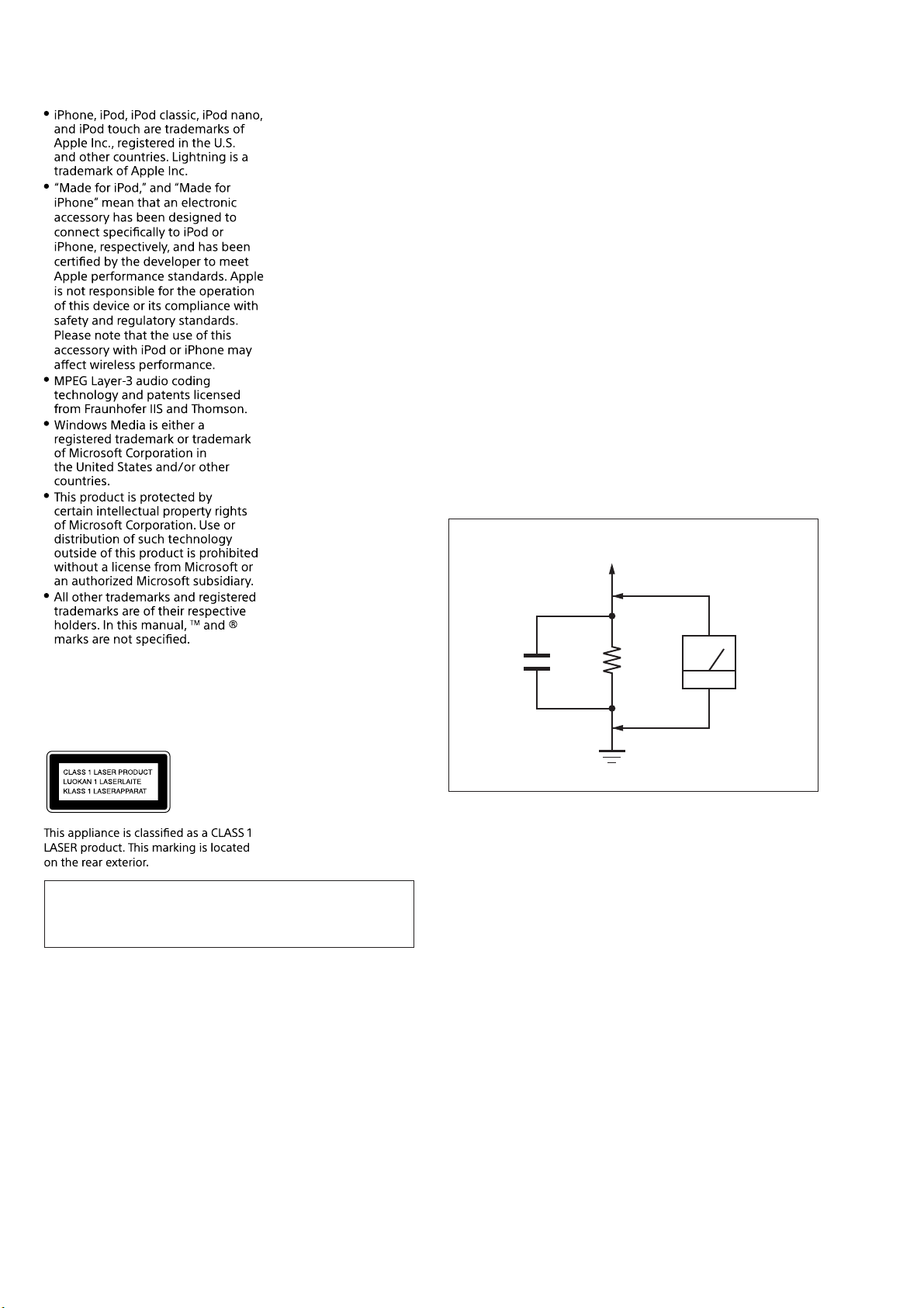
CAPACITOR ELECTRICAL DISCHARGE PROCESSING
When checking the board, the electrical discharge is necessary for
the electric shock prevention.
Connect the resistor to both ends of respective capacitors.
• POWER Board
CE503, CE504
– POWER Board (Conductor Side) –
800 :/2 W
(for CE503)
800 :/2 W
(for CE504)

HCD-EC719iP/EC919iP
5
MODEL IDENTIFICATION
Distinguish by model number label stuck on the rear side of a main unit.
Note: The printed contents of following figure model number label may be different from the model number label of a main unit.
– Rear view –
MODEL NUMBER LABEL
HCD-EC919iP: US model
HCD-EC919iP: Canadian model
HCD-EC719iP: AEP and UK models

HCD-EC719iP/EC919iP
6
HOW TO EJECT THE DISC WHEN POWER SWITCH TURN OFF
SERVICE POSITION
3Pull out the disc tray.
1Refer to “SECTION 2. DISASSEMBLY” (page 7), remove the side cover,
the top cover block and the rear panel block from the unit.
– Rear view –
2Turn the traverse gear in
the direction of an arrow.
bottom side
top side
– Rear view –
MAIN board
POWER board
FRONT board
USB board
insulating sheet

HCD-EC719iP/EC919iP
7
SECTION 2
DISASSEMBLY
• This set can be disassembled in the order shown below.
2-1. DISASSEMBLY FLOW
2-2. SIDE COVER,
TOP COVER BLOCK
(Page 8)
SET
2-3. POWER CORD (AC1),
REAR PANEL BLOCK
(Page 9)
2-4. CD DOOR
(Page 10)
2-6. MAIN BOARD BLOCK
(Page 11)
2-8. POWER BOARD
(Page 12)
2-7. MAIN BOARD
(Page 11)
2-10. USB BOARD
(Page 14)
2-11. LOADER WITH FFC (TDL-5) (CDM1)
(Page 14)
2-9. FRONT BOARD
(Page 13)
2-5. FRONT PANEL BLOCK
(Page 10)

HCD-EC719iP/EC919iP
8
Note: Follow the disassembly procedure in the numerical order given.
2-2. SIDE COVER, TOP COVER BLOCK
3
3
7Remove the top cover block
in the direction of an arrow.
8top cover block
2five claws
5connector
(XP8)
2two claws
2five claws
4right side cover
4left side cover
6four claws
2two claws
2two claws
2two claws
WireVeWWiQJ
1rear screw
(black 3 u8)
1rear screw
(black 3 u8)
1rear screw
(black 3 u8) 1rear screw
(black 3 u8)
1rear screw
(black 3 u8)
1rear screw
(black 3 u8)

HCD-EC719iP/EC919iP
9
2-3. POWER CORD (AC1), REAR PANEL BLOCK
5connector
(XP16)
4fan connector
(XP14)
7claw
7claw
9rear panel block
8Remove the rear panel block
in the direction of an arrow.
1power cord connector
(CN501)
3power cord
(AC1)
– Rear view –
7claw
7claw
(EC919iP)
OK
NG
Note 2: When installing the rear
panel block, check that
jacks are properly secured.
Jacks are fitted to
the surface.
Jacks has been
depressed.
6screw
(silver 3 u8)
6screw
(silver 3 u8)
6screw
(silver 3 u8)
2
Power cord setting
– Rear view –
Note 1: When installing the power cord (AC1),
check the direction of connector.

HCD-EC719iP/EC919iP
10
2-5. FRONT PANEL BLOCK
2-4. CD DOOR
4CD door
3four claws
2Pull out the disc tray.
– Rear view –
1Turn the traverse gear in
the direction of an arrow.
bottom side
top side
– Rear view –
4two claws
4two claws
5front panel block
– Rear right view –
3connector
(XP15)
2connector
(XP7)
1connector
(XP19)
Wire setting
Wire from USB board
is upper.
Wire from FRONT board
is lower.
– Right view –
MAIN board
heatsink
front panel block
resistor
Note: When installing the wire,
be careful not to touch the
resistor.

HCD-EC719iP/EC919iP
11
2-7. MAIN BOARD
2-6. MAIN BOARD BLOCK
5Solder the short-land.
Note 2: When assembling the MAIN board block,
remove the solder of short-land after
connecting all flexible flat cable
and connector.
2connector
(XP4)
6flexible flat cable
(XP3)
7MAIN board block
4Lift the MAIN board block
in the direction of an arrow.
1connector (XP5)
Note 3: Since the wire is very thin, it is easy to cut.
When disconnecting, do it while holding the
connector part.
3two claws
3two claws
3four claws
Note 1: Before disconnecting the flexible flat cable of the loader with FFC (TDL-5) (CDM1), solder the short-land.
7MAIN board
2connector
(XP2)
1connector
(XP1)
– Rear right view –
3screw
(silver 3 u8)
3screw
(silver 3 u8)
3two screws
(silver 3 u8)
6heatsink
5three heat sink
screws
(3 u8)
5heat sink
screw
(3 u8)
4Remove the MAIN board block
in the direction of an arrow.
(EC919iP)

HCD-EC719iP/EC919iP
12
2-8. POWER BOARD
– Rear view –
0POWER board
2connector
(XP2)
1connector
(XP1)
9Draw out the
wires. 8Remove the power board
in the direction of an arrow.
6ECL7/9 shield cover
5
– Rear view –
4six claws
4claw
3screw
(silver 3 u8)
7screw
(silver 3 u8)
7screw
(silver 3 u8)
7two screws
(silver 3 u8)

HCD-EC719iP/EC919iP
13
2-9. FRONT BOARD
2two screws
(silver 3 u8)
2two screws
(silver 3 u8)
3ground plate
5FRONT board
4two claws
1VOL knob
(plating)
– Front panel block rear view –
2screw
(silver 3 u8)
2screw
(silver 3 u8)
FRONT board
Wire setting
– Front panel block rear view –
FRONT board
Wire setting
– Front panel block rear view –

HCD-EC719iP/EC919iP
14
2-10. USB BOARD
2-11. LOADER WITH FFC (TDL-5) (CDM1)
3USB board
– Front panel block rear view –
2ground plate
Wire setting FRONT board
USB board
– Front panel block rear view –
1USB PWB screw
(2.6 u8)
1USB PWB screw
(2.6 u8)
2loader with FFC (TDL-5)
(CDM1)
– Bottom view –
1screw
(silver 3 u8)
1screw
(silver 3 u8)
Note: The wire is soldered to the
terminal of the switch.
Be careful so that not cut
or bend the terminal.

HCD-EC719iP/EC919iP
HCD-EC719iP/EC919iP
1515
SECTION 3
TEST MODE
SOFTWARE VERSION
It can confirm the software version.
Procedure:
1. Press the [?/1] button to turn the power on.
2. Press the [Z] button to open the disc tray.
3. Press the button on the remote commander as following order.
[CLEAR] →[B] →[RETURN]
(Displayed values in the following figure are example)
R1395P28
Screen display
MCU version MPEG version
Model Region
Model
Model Display
HCD-EC719iP 7
HCD-EC919iP 9
4. The software version display disappears in about 5 seconds,
and it returns to the display of the normal mode.
FACTORY RESET
It can clear all data including preset data stored in the memory to
initial conditions. Execute this mode when returning the this unit
to the customer.
Procedure:
1. Press the [?/1] button to turn the power on.
2. Press two buttons of the [x] and [EQ] simultaneously for five
seconds.
3. The message “RESET OK” is displayed on the fluorescent in-
dicator tube, then returns to the normal mode.
TRAY LOCK
It can be unable to take sample disc out of disc tray in the shop.
Procedure:
1. Press the [?/1] button to turn the power on.
2. Press the [Z] button to open the disc tray.
3. Set a disc on the disc tray.
4. Press the [Z] button to close the disc tray.
5. Press two buttons of the [x] and [Z] simultaneously for five
seconds.
6. The message “LOCKED” is displayed on the fluorescent indi-
cator tube and the disc tray is locked.
(Even if pressing the [Z] button, the message “LOCKED” is
displayed on the fluorescent indicator tube and the disc tray is
locked)
Releasing method:
1. Press two buttons of the [x] and [Z] simultaneously for five
seconds.
2. The message “UNLOCKED” is displayed on the fluorescent
indicator tube and the disc tray is unlocked.
CHILD LOCK
It can lock except for the [?/1] button of a main unit to prevent
from being operated by mistake.
Procedure:
1. Press the [?/1] button to turn the power on.
2. Press the [x] button for five seconds.
3. The message “LOCK ON” is displayed on the fluorescent indi-
cator tube and the except for the [?/1] button is locked.
(Even if pressing except for the [?/1] button, the message
“LOCK ON” is displayed on the fluorescent indicator tube and
the operation is locked)
Releasing method:
1. Press the [x] button for five seconds.
2. The message “LOCK OFF” is displayed on the fluorescent in-
dicator tube and the all buttons are unlocked.
Note: This mode is not released even if it unplugs a power cord.
VFD TEST
It can confirm the fluorescent indicator tube.
Procedure:
1. Press the [?/1] button to turn the power on.
2. Press two buttons of the [x] and [ENTER] simultaneously for
five seconds.
3. All segments on the fluorescent indicator tube light up.
Screen display
4. All segments turn off the light in about 3 seconds, and it re-
turns to the display of the normal mode.
SECTION 4
ELECTRICAL CHECK
CD SECTION
Note:
1. CD block is basically constructed to operate without adjustment.
2. Use YEDS-18 disc (Part No. 3-702-101-01) unless otherwise indicat-
ed.
3. Use an oscilloscope with more than 10 Mimpedance.
4. Clean the object lens by an applicator with neutral detergent when the
signal level is low than specified value with the following check.
RF SIGNAL CHECK
+
–
MAIN board
TP27 (PUHRF)
TP31 (VREF1)
oscilloscope
(DC range)
Procedure:
1. Connect the oscilloscope to TP27 (PUHRF) and TP31
(VREF1) on the MAIN board.
2. Press the [?/1] button to turn the power on.
3. Press the [FUNCTION] button to turn the CD function.
4. Press the [Z] button to open the disc tray.
5. Set the disc (YEDS-18) on the disc tray.
6. Press the [Z] button to close the disc tray.
7. Press the [u] button to playback.
8. Confirm that oscilloscope waveform is as shown in the figure
below. (eye pattern)
A good eye pattern means that the diamond shape () in the
center of the waveform can be clearly distinguished.
VOLT/DIV: 200 m
V
TIME/DIV: 400 ns
level: 1.2 ± 0.2 Vp-p
Connection Location:
TP31
(VREF1)
TP27
(PUHRF)
– MAIN Board (Conductor Side) –
TP31
(VREF1)
TP27
(PUHRF)

HCD-EC719iP/EC919iP
HCD-EC719iP/EC919iP
1616
SECTION 5
DIAGRAMS
5-1. BLOCK DIAGRAM
MCU
STM8S003K3
IR
2*I/O
5V
SDRAM
64M(Byte)
FLASH
2M(Byte)
LOADER
TDL-5+IM OPU
Moto driver IC
AM5890
AUDIO
SW IC
74HC4052
CP 2.0C
I2C
VFD
Audio IN
FM/AM
I2C
SPI
IR
ADC
data
Over
USB
Ipod
Lightning
USB
RTC
KEY
Power KEY
I2C
USB S/W
*0
I/O
UART
+
-
+
-
INT
USB
protect
SPI
I2C
AUDIO
PROCESSOR
AMP
STA516B
PWM
PBTL
I2S
VOLUME
OP
MPEG Decoder
SPHE8104WW(CD)
/
SPHE8202W(DVD)
Power derating
AMP
STA516B
AMP
STA516B
CVBS
DVD Model
Model with Dock
Model with SW

HCD-EC719iP/EC919iP
HCD-EC719iP/EC919iP
1717
For Schematic Diagrams.
Note:
• All capacitors are in μF unless otherwise noted. (p: pF) 50
WV or less are not indicated except for electrolytics and
tantalums.
• All resistors are in Ωand 1/4 W or less unless otherwise
specified.
THIS NOTE IS COMMON FOR PRINTED WIRING BOARDS AND SCHEMATIC DIAGRAMS.
(In addition to this, the necessary note is printed in each block.)
For Printed Wiring Boards.
Note:
• : Pattern from the side which enables seeing.
(The other layers’ patterns are not indicated.)
Caution:
Pattern face side:
(Conductor Side)
Parts face side:
(Component Side)
Parts on the pattern face side seen
from the pattern face are indicated.
Parts on the parts face side seen from
the parts face are indicated.
• Circuit Boards Location
USB board
DOCKING board POWER board
FRONT board
TUNER board
MAIN boar
d
Note: The components identified by mark 0or dotted
line with mark 0are critical for safety.
Replace only with part number specified.
Note: Les composants identifiés par une marque 0sont
critiques pour la sécurité.
Ne les remplacer que par une piéce portant le nu-
méro spécifié.

HCD-EC719iP/EC919iP
HCD-EC719iP/EC919iP
1818
5-2. PRINTED WIRING BOARD - MAIN Board -
MAIN BOARD (COMPONENT SIDE) MAIN BOARD (CONDUCTOR SIDE)
A
B
C
D
E
1 2 3 4 5 6 7 8 9 10 11 12
F
G
• : Uses unleaded solder.
• See page 17 for Circuit Boards Location.
Other manuals for MHC-EC619iP
2
This manual suits for next models
8
Table of contents
Other Sony Stereo System manuals

Sony
Sony NAS-CZ1 M-Crew User manual

Sony
Sony CMT-HX3 User manual

Sony
Sony HCD-SHAKE33 User manual

Sony
Sony HCD-GNX60 User manual

Sony
Sony CMT-HX3 User manual

Sony
Sony S2 Sports ZS-X10 User manual

Sony
Sony SAV-E525 User manual

Sony
Sony LBT-D670AV - Compact Hifi Stereo System User manual

Sony
Sony HCD-VX90AV User manual

Sony
Sony WX-900BT User manual