ST EVSPIN958 User manual

Introduction
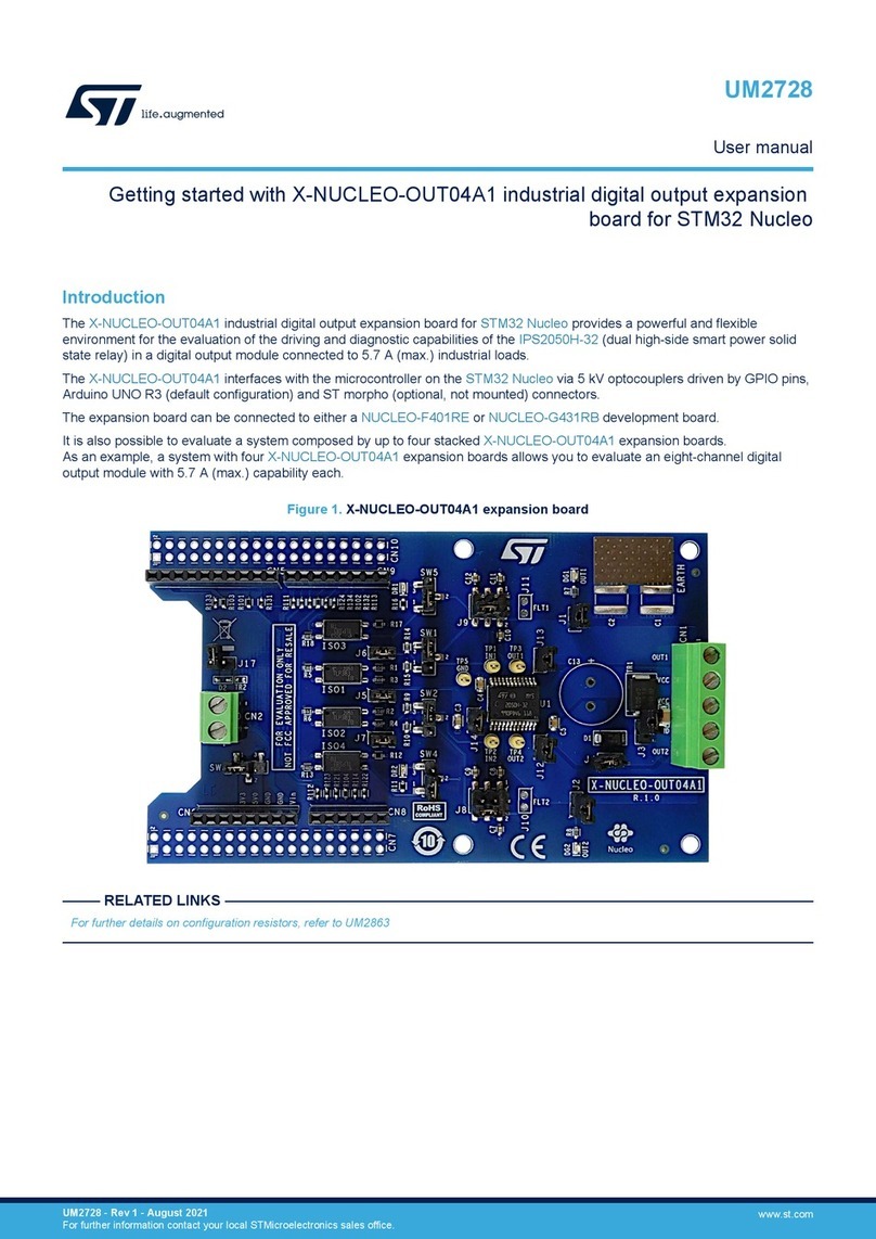
The EVSPIN958 single brushed DC motor driver expansion board is based on the STSPIN958.
It provides an affordable and easy-to-use solution for the implementation of brushed DC motor driving applications. Thanks
to the parallel operation, it can be easily converted to a single half-bridge with double current capability. In addition to the
internal current limiter, the integrated amplifiers allow it to be used in systems with external current control. The EVSPIN958 is
compatible with the Arduino UNO R3 connector and most STM32 Nucleo boards.
Figure 1. EVSPIN958 expansion board
Getting started with the EVSPIN958 brushed DC motor driver expansion board
based on the STSPIN958
UM3056
User manual
UM3056 - Rev 1 - September 2022
For further information contact your local STMicroelectronics sales office.
www.st.com

1Safety precautions
Warning: Some of the components mounted on the board could reach hazardous temperatures
during operation.
While using the board, please follow the following precautions:
• Do not touch the components or the heatsink.
• Do not cover the board.
• Do not put the board in contact with flammable materials or with materials releasing smoke when heated.
• After operation, allow the board to cool down before touching it.
UM3056
Safety precautions
UM3056 - Rev 1 page 2/18

2Getting started
The main features of the EVSPIN958 expansion board are:
• Voltage range from 5 V to 58 V
• Phase current up to 5 A r.m.s
• Adjustable output slew rate
• Seven different driving modes
• One current limiter with adjustable OFF time
• Two integrated amplifiers with fixed gain
• Full protection set including: overcurrent, undervoltage lock out and thermal shutdown
• Compatibility with Arduino UNO R3 connector and STM32 Nucleo boards
The EVSPIN958 evaluation board is ready to be used in few steps. Follow this procedure to start your evaluation:
1. Check the setting of the jumpers based on your configuration as described in Section 3
2. Connect the board with the STM32 Nucleo board through the Arduino UNO R3
3. Supply the board through the input 2 (VS) and 1 (ground) of the connector CN1
Further support material is available on the STSPIN958 product page www.st.com
UM3056
Getting started
UM3056 - Rev 1 page 3/18

3Hardware description and configuration
Figure 2. EVSPIN958 overview
The following tables provide the detailed pinout of the Arduino UNO R3 and ST Morpho connectors.
Table 1. Arduino UNO R3 connector table
Connector Pin(1) Signal Remarks
CN5
2 Operational amplifiers offset enable
3 Standby (active low)
6 Operational amplifier 1 output
7 Ground
CN9
3 Voltage reference current limiter
5 PWM1 input
7 Enable bridge
CN6
2 VDD
6 Ground
7 Ground
CN8
2 PWM2 input
3 TOFF signal Digital output in
PWM trimming mode
6 Operational amplifier 2 output
1. All non-listed pins are not connected.
3.1 Driving mode selection
The EVSPIN958 can drive up to 2 DC motors at the same time.
UM3056
Hardware description and configuration
UM3056 - Rev 1 page 4/18

The driving mode selection is done setting J1 and J2 jumpers (connected to MODE1 and MODE2 pins of the
device) on the top of the board.
J6 solder jumper on the bottom of the board must be closed/opened according to the selected driving mode.
The table below briefly summarizes the possible configurations:
Table 2. Driving mode settings
J1 J2 Driving
mode
Typical
application J6(1)
Max.
output
current
(each
motor)
Output
RDS(ON
)
Minimu
m OCD
threshol
d
1-2 1-2 Dual half-
bridge
2 x unidirectional
brushed DC
(Figure 3)
open
5 Arms
0.2Ω
7 A
1 x bidirectional
brushed DC
(Figure 4)
closed 0.4Ω
1-2 2-3 Single full-
bridge
1 x bidirectional
Figure 4 closed 5 Arms 0.4Ω 7 A
2-3 1-2 Single half-
bridge
1 x high current
unidirectional
brushed DC(2)
(Figure 5)
closed 10 Arms 0.2Ω 14 A
2-3(3) 2-3(3)
Single full-
bridge with
mixed decay
1 x bidirectional
brushed DC
or
Half bipolar
stepper
(Figure 4)
closed 5 Arms 0.4Ω 7 A
1. When J6 is closed, the removal of the shunt resistor 2 (R9) is recommended for higher precision of the triggering of the
current limiter
2. The motor can be connected between OUT and either LSS (like in the figure) or VS, paying attention to properly connect
PWM2 to GND or to VDD respectively.
3. This configuration is only available with current limiter in Fixed OFF time mode (see Section 3.2 ).
UM3056
Driving mode selection
UM3056 - Rev 1 page 5/18

Figure 3. Two unidirectional DC motors
OUT2
OUT1
M
M
VVS
GND
+
UM3056
Driving mode selection
UM3056 - Rev 1 page 6/18

Figure 4. One bidirectional DC motor
OUT2
OUT1
M
VVS
GND
+
UM3056
Driving mode selection
UM3056 - Rev 1 page 7/18

Figure 5. One unidirectional DC motors – higher current
OUT2
OUT1
M
VVS
GND
+
3.2 Current limiter mode
The behavior of the current limiter can be changed by setting the J3 jumper (connected to MODE3 of the device)
as follows:
Table 3. Current limiter mode settings
J3 Current limiter mode J5 and J3 Decay time
1-2 Fixed OFF time Closed Depending on R6 resistor
(Figure 6)
2-3 PWM trimming Open Depending on PWM input signals
In Fixed OFF time mode, the current limiter can be disabled by setting R6 to its minimum value.
The current threshold can be set in two different ways:
• Trimming R13 resistor, leaving CN9.3 floating
• Applying a square wave with variable duty cycle to CN9.3, setting R13 to its minimum value
UM3056
Current limiter mode
UM3056 - Rev 1 page 8/18

Figure 6. tOFF versus ROFF
3.3 Output slew rate
The output slew rate can be increased moving the rotative switch SW1 clockwise. With the STSPIN958 device,
the slew rate value can be chosen from four different values, as shown in Table 4.
Table 4. Slew rate settings
SW1 RSR Slew rate (typ. at VS = 58 V)
C-1 closed 10 kΩ 0.3 V/ns
C-2 closed 5.6 kΩ 0.6 V/ns
C-3 closed 2.2 kΩ 1.2 V/ns
C-4 closed 1 kΩ 2 V/ns
UM3056
Output slew rate
UM3056 - Rev 1 page 9/18

4Thermal performance
An example of the thermal performances of the EVSPIN958 is provided in Figure 7 . The board is used in
full-bridge and parallel half-bridge configuration in a typical application to drive an inductive load with different
output currents ranging from 0.5 A to 4 A.
Set-up conditions:
•Planar orientation of the board and natural convection only
•Tambient = 25 °C
•PWM frequency = 20 KHz
•VS = 30 V
•Output slew rate setting = 2 V/ns
Figure 7. EVSPIN958 - thermal performances
0
20
40
60
80
100
120
140
160
0 1 2 3 4
Maximum
temperature [°C]
Output current [ARMS]
Parallel half bridge
Full bridge
Figure 8. Thermal images (IOUT = 2ARMS)
Full-bridge configuration Parallel half-bridge configuration
UM3056
Thermal performance
UM3056 - Rev 1 page 10/18

5Bills of material
Table 5. EVSPIN958 bill of material
Item Qty. Ref. Description Part/Value Manufact. Order code
1 1 CN1 Connector 5.08 mm Close Vertical MORSV-508-2P_
screw
Wurth
Elektronik
691312510002 or
equivalent
2 1 CN2 Connector 5.08 mm close vertical MORSV-508-4P_
screw
Wurth
Elektronik
691312510004 or
equivalent
3 1 CN5 Connector through-hole-pitch 2.54 CON-1x10 Samtec SSQ-110-04-F-S
4 2 CN6,CN9 Connector through-hole-pitch 2.54 CON-1x8 Samtec SSQ-108-04-F-S
5 2 CN7,CN10 Connector through-hole-pitch 2.54 N.M. Samtec ESQ-119-24-G-D
6 1 CN8 Connector through-hole-pitch 2.54 CON-1x6 Samtec SSQ-106-04-F-S
7 2 C1,C8 SMT ceramic capacitor 100 n 15 V
8 1 C2 SMT ceramic capacitor 1 u 15 V
9 2 C3,C4 Through-hole aluminum elect.
capacitor 220 u 100 V Panasonic EEUFS2A221B
10 1 C5 SMT ceramic capacitor 220 n 15 V
11 2 C6,C7 SMT ceramic capacitor 1 n 15 V
12 2 C9,C10 SMT ceramic capacitor 100 p 15 V
13 1 C11 SMT ceramic capacitor 10 n 15 V
14 2 C12,C13 SMT ceramic capacitor 470 n 100 V
15 1 C14 SMT ceramic capacitor 100 n 100 V
16 2 D1,D2 Yellow LED Yellow
17 1 D3 Red LED Red
18 1 SW1 Rotative switch x4 ROT-SWITCH Nidec CS-4-14-NTB or
equivalent
19 3 J1,J2,J3 Header connector 1x3 pins Closed 1-2
21 1 J5 Header connector 1x2 pins Closed
22 1 J6 Solder jumper Open
23 2 Q1,Q2 P MOSFET MOSFET P NXP NX3008PBKW
24 1 R1 SMT resistor 22 k 1/10 W
25 2 R2,R20 SMT resistor 1 k 1/10 W
26 1 R3 SMT resistor 2.2 k 1/10 W
27 1 R4 SMT resistor 5.6 k 1/10 W
28 2 R5,R15 SMT resistor 10 k 1/10 W
29 1 R6 1/4" square trimpot trimming
potentiometer, top adjust 500 k Bourns 3266W-1-504 LF
30 2 R7,R8 SMT resistor 4.7 k 1/10 W
31 2 R9,R10 SMT resistor 0.05 1% 3 W Bourns CRA2512-FZ-
R050ELF
32 1 R11 SMT resistor 47 k 1/10 W
33 2 R12,R17 SMT resistor 330 R 1/10 W
34 1 R13 1/4" square trimpot trimming
potentiometer, top adjust 1 k Bourns 3266W-1-102 LF
35 1 R14 SMT resistor 3.3 k 1/10 W
UM3056
Bills of material
UM3056 - Rev 1 page 11/18

Item Qty. Ref. Description Part/Value Manufact. Order code
36 1 R16 SMT resistor 39 k 1/10 W
37 2 R18,R19 SMT resistor 10 k ½ W
38 9
R21,R22,R23
R24,R25,R26
R27,R28,R29
SMT resistor 0 R 1/10 W
39 9
TP1,TP2,TP3
TP4,TP5,TP6
TP7,TP8,TP9
Test point TP-SMD-
S1751-46R Harwin S1751-46R
40 1 U1 STSPIN958 STSPIN958
UM3056
Bills of material
UM3056 - Rev 1 page 12/18

6Schematic diagrams
Figure 9. EVSPIN958 schematic diagram
ST
NUCLEO & LOGO
FOR EVALUATION PURPOSE ONLY
ROHS COMPLIANT 2002/95/IEC & LOGO
PWM2/PH
PWM1
REF
OUT1
OUT2
VDD
GND GND
VS 0 - 58V
VS
GND
EN
STBY
OFFSET
V1
TOFF
V2
REF
M1 M2 M3
REF
TOFF
V2
V1
LSS2
LSS1
SR
V1
nS TDBY
OFFSE T
EN_nFAULT
EN_MCU
nS TDBY
PWM1
PWM2
PWM1
PWM2
EN_nFAULT
EN_MCU
MODE1
MODE1 MODE2
REF
OFFSE T
OUT2
OUT1
TOFF
V2
REF_MCU
LSS 2
LSS 1
REF_MCU
MODE2
MODE3
MODE3
V2V1
TOFF
REF
OUT1
OUT2
LSS 1
LSS 2
VDD VDD
VDD
VDD VDD
VS
VS
VDD
VDD
VDD
U1
STSP IN958
OUT2 25
LSS 2 24
VS 27
VS 28
OUT2 26
LSS 2 23
OUT1 32
OUT1 31
LSS 1 2
LSS 1 1
VS 30
VS 29
VSP UMP 4
CP 2 6
CP 1 5
VBOOT 7
nS TDBY
10
EN/nF AULT
14
PWM1
11
PWM2
12
VDD 13
REF
15
MODE3
18
TOFF
16
MODE1
20
MODE2
19
SR
21
GNDP UMP
3
GND
22
EP AD
33
OFFSE T
9
V1
8
V2
17
R6
500k
CN8
CON-1x6
STRIP25 4P -F-6
1
2
3
4
5
6
R510k
C9
100p
R1
22k
C1
100n
CN7
CON-2x19
1
3
5
7
9
11
13
15
17
19
21
23
25
27
29
31
33
35
37
2
4
6
8
10
12
14
16
18
20
22
24
26
28
30
32
34
36
38
C13
470n
TP3
R2
1k D2
YELLOW
1 2
TP8
TP2
C6
1n
R18
10K
CN1
1
2
J2
CON3
1
2
3
D3
Re d
1 2
R27 0R
R14
3.3 k
CN9
CON-1x8
1
2
3
4
5
6
7
8
R21 0R
C7
1n
R15
10k
R24 0R
CN6
CON-1x8
STRIP25 4P -F-8
1
2
3
4
5
6
7
8
R7
4.7 k
D1
YELLOW
1 2
R13
1k
C11
10n
J3
CON3
1
2
3
R17
330R
C5
220n
R12
330R
R9
0.0 5R 3 W
R3
2.2 k
R20 1k
Q2
MOSFET P
2
1
3
TP5
J1
CON3
1
2
3
C14
100n
C12
470n
C8
100n
R8
4.7 k
R29 0R
TP6
R23 0R
TP9
R11
47k
C3
220u
CN5
CON-1x10
1
2
3
4
5
6
7
8
9
10
C2
1u
R28 0R
R25 0R
J6
1 2
R4
5.6 k
J5
1
2
TP7
R10
0.0 5R 3 W
C10
100p
R16
39k
CN2
1
2
3
4
TP4
C4
220u
Q1
MOSFET P
2
1
3
R19
10K
R22 0R
R26 0R
CN10
CON-2x19
1
3
5
7
9
11
13
15
17
19
21
23
25
27
29
31
33
35
37
2
4
6
8
10
12
14
16
18
20
22
24
26
28
30
32
34
36
38
SW1
4
3
2
NC
C
1
TP1
UM3056
Schematic diagrams
UM3056 - Rev 1 page 13/18

Revision history
Table 6. Document revision history
Date Version Changes
14-Sep-2022 1 Initial release.
UM3056
UM3056 - Rev 1 page 14/18

Contents
1Safety precautions.................................................................2
2Getting started ....................................................................3
3Hardware description and configuration ...........................................4
3.1 Driving mode selection ..........................................................4
3.2 Current limiter mode ............................................................8
3.3 Output slew rate ...............................................................9
4Thermal performance .............................................................10
5Bills of material...................................................................11
6Schematic diagrams ..............................................................13
Revision history .......................................................................14
List of tables ..........................................................................16
List of figures..........................................................................17
UM3056
Contents
UM3056 - Rev 1 page 15/18

List of tables
Table 1. Arduino UNO R3 connector table .........................................................4
Table 2. Driving mode settings .................................................................5
Table 3. Current limiter mode settings ............................................................8
Table 4. Slew rate settings ...................................................................9
Table 5. EVSPIN958 bill of material ............................................................ 11
Table 6. Document revision history ............................................................. 14
UM3056
List of tables
UM3056 - Rev 1 page 16/18

List of figures
Figure 1. EVSPIN958 expansion board .........................................................1
Figure 2. EVSPIN958 overview ...............................................................4
Figure 3. Two unidirectional DC motors ..........................................................6
Figure 4. One bidirectional DC motor ...........................................................7
Figure 5. One unidirectional DC motors – higher current ..............................................8
Figure 6. tOFF versus ROFF ..................................................................9
Figure 7. EVSPIN958 - thermal performances .................................................... 10
Figure 8. Thermal images (IOUT = 2ARMS)...................................................... 10
Figure 9. EVSPIN958 schematic diagram ....................................................... 13
UM3056
List of figures
UM3056 - Rev 1 page 17/18

IMPORTANT NOTICE – READ CAREFULLY
STMicroelectronics NV and its subsidiaries (“ST”) reserve the right to make changes, corrections, enhancements, modifications, and improvements to ST
products and/or to this document at any time without notice. Purchasers should obtain the latest relevant information on ST products before placing orders. ST
products are sold pursuant to ST’s terms and conditions of sale in place at the time of order acknowledgment.
Purchasers are solely responsible for the choice, selection, and use of ST products and ST assumes no liability for application assistance or the design of
purchasers’ products.
No license, express or implied, to any intellectual property right is granted by ST herein.
Resale of ST products with provisions different from the information set forth herein shall void any warranty granted by ST for such product.
ST and the ST logo are trademarks of ST. For additional information about ST trademarks, refer to www.st.com/trademarks. All other product or service names
are the property of their respective owners.
Information in this document supersedes and replaces information previously supplied in any prior versions of this document.
© 2022 STMicroelectronics – All rights reserved
UM3056
UM3056 - Rev 1 page 18/18
Table of contents
Other ST Computer Hardware manuals

ST
ST STEVAL-ISF001V1 User manual

ST
ST STM32 Nucleo User manual

ST
ST X-NUCLEO-OUT16A1 User manual

ST
ST STEVAL-IFP043V1 User manual

ST
ST X-NUCLEO-IHM07M1 User manual

ST
ST UM2033 User manual

ST
ST X-NUCLEO-6283A1 User manual

ST
ST STEVAL-DPSG474 User manual

ST
ST STM32F4 Series Owner's manual

ST
ST I-CUBE-LRWAN User manual

ST
ST X-NUCLEO-IHM11M1 User manual

ST
ST STM32 Nucleo User manual

ST
ST X-NUCLEO-IOD02A1 User manual

ST
ST X-NUCLEO-EEPRMA2 User manual

ST
ST X-NUCLEO-OUT14A1 User manual

ST
ST CLT01-38SQ7 User manual

ST
ST X-CUBE-CELLULAR User manual

ST
ST STEVAL-IFP047V1 User manual

ST
ST X-NUCLEO-IHM17M1 User manual

ST
ST STEVAL-IDZ3V1 Series User manual