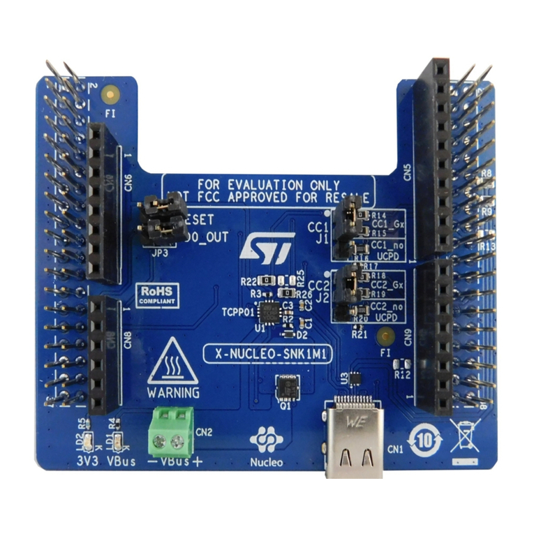
ST X-NUCLEO-DRP1M1 User manual

Introduction
The X-NUCLEO-DRP1M1 expansion board allows evaluating the features of TCPP03-M20 and the USB Type-C™ features and
protections required for VBUS and CC lines suitable for dual role power (DRP) applications.
The expansion board can be stacked on top of any STM32 Nucleo-64 with Power Delivery (UCPD) peripheral embedded in their
microcontrollers.
The X-NUCLEO-DRP1M1 effectively demonstrates the dead battery and Sink operation, thanks to the integrated ST715PU33R
LDO linear regulator that supplies the connected STM32 Nucleo development board. It also demonstrates USB Type-C™
Source operation when a compatible external Source is connected to the board.
Moreover, the expansion board allows Dual Role Data functionalities for sourcing devices.
The X-NUCLEO-DRP1M1 is compliant with the USB Type-C™ and Power Delivery specifications 3.1 standard power range
(SPR) and is USB-IF certified as a 100 W DRP solution supporting programmable power supply (PPS).
The companion software package (X-CUBE-TCPP) contains the application examples for development boards embedding
UCPD-based microcontrollers (NUCLEO-G071RB, NUCLEO-G474RE and NUCLEO-G0B1RE).
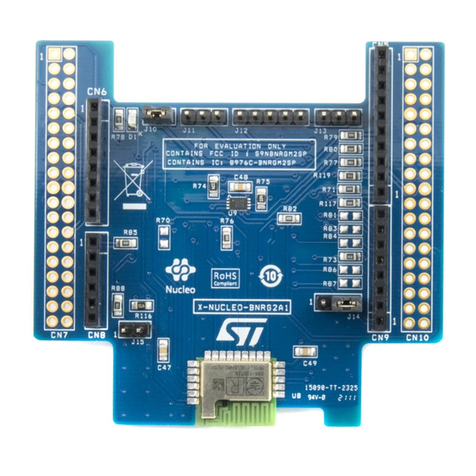
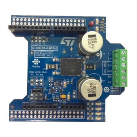
Figure 1. X-NUCLEO-DRP1M1 expansion board
Getting started with the X-NUCLEO-DRP1M1 USB Type-C™ Power Delivery
dual role port expansion board based on TCPP03-M20 for STM32 Nucleo
UM2891
User manual
UM2891 - Rev 1 - June 2021
For further information contact your local STMicroelectronics sales office.
www.st.com

1Getting started
1.1 Overview
The X-NUCLEO-DRP1M1 expansion board features:
• Support for all USB Type-C™ Power Delivery SPR profiles up to 100 W
• Management of Dual Role Data/Power configuration
• USB 2.0 Dual Role Data compliant according to STM32 USB data capability
• 8/20 μs surge, overvoltage, overcurrent protection and discharge for VBUS
• Short to VBUS protection for CC1 and CC2 configuration channel pins
• ESD protection (IEC61000-4-2 level 4 ± 8 kV contact discharge) for CC1, CC2, D+ and D-
• Overvoltage, overcurrent protection and discharge for VCONN
• Common mode filter on D+/D- data lines
• Three power modes to optimize current consumption
• Compliant with Programmable Power Supplies (PPS)
• Free comprehensive development firmware library
• Compliant with STM32 Nucleo-64 boards featuring an STM32 with UCPD
The X-NUCLEO-DRP1M1 interfaces three main blocks for USB Type-C™ Power Delivery dual role port (DRP):
• Type-C™ connector
• the power delivery controller embedded into the STM32 (UCPD) on the STM32 Nucleo development board
and
• the power management
It also provides USB 2.0 data line interface connection to the STM32 on the STM32 Nucleo development board.
The bill of materials has been optimized without compromising the protection:
• VBUS line: overvoltage, overcurrent and surge protections
• CC lines: overvoltage, overcurrent and ESD protections
• Data lines: ESD protection and EMI filtering
The embedded TCPP03-M20 features comply with the Power Delivery protocol:
• CC lines switch matrix for VCONN
• VBUS discharge
• VCONN discharge
Fault mode report and three optimized power modes are also available.
All these features are managed through I²C communication.
VBUS current analog readout is also possible with STM32 ADC connected to the TCPP03-M20 differential
amplifier output.
UM2891
Getting started
UM2891 - Rev 1 page 2/27

Figure 2. X-NUCLEO-DRP1M1 board on top of STM32 Nucleo development board block diagram (full lines
identify Type-C™ connector connections/dotted lines identify internal connections)
UCPD
STM32
Firmware
I2C
USB Type-C™
connector
VBUS
Power bus
Provider path
CC1/CC2 lines
D+/D- lines
Configuration channels
N-MOSFET
SOURCE
N-MOSFET
SINK
Consumer path
USB 2.0
Data lines
Protections
NUCLEO board
X-NUCLEO-DRP1M1 board
ADC
TCPP03-M20
1.2 Hardware architecture
The X-NUCLEO-DRP1M1 expansion board can be used with any STM32 Nucleo-64 development board
embedding the UCPD peripheral (mainly NUCLEO-G071RB, NUCLEO-G474RE and NUCLEO-G0B1RE).
The expansion board must be plugged on the matching pins of the development board CN7 and CN10 ST
morpho connectors.
When plugged onto an STM32 Nucleo development board, the expansion board can be supplied in two different
ways:
• through the STM32 Nucleo ST-LINK supply using the development board internal LDO
• by the VBUS provided when a Source is plugged into the CN1 USB Type-C™ connector and thanks to the
integrated ST715PU33R LDO linear regulator (U2) that supplies the entire system, which supports Dead
Battery operation mode and source powered mode.
UM2891
Hardware architecture
UM2891 - Rev 1 page 3/27

Figure 3. X-NUCLEO-DRP1M1 main functional blocks (top view)
1-2. Morpho connectors
3-6. Arduino connectors
7. Type-C™ connector
8. Provider path screw connector plus LED
9. Consumer path screw connector plus LED
10. 3.3 V LED
11. Jumpers for self-powering (LDO out plus NRST)
12. TCPP03-M20 - USB-C DRP protection
13. ECMF02-2AMX6 - common mode filter plus ESD protection
14. ESDA25P35-1U1M - TVS diode
12
3
4
5
6
78 9
10
11
12 13
14
UM2891
Hardware architecture
UM2891 - Rev 1 page 4/27

Figure 4. X-NUCLEO-DRP1M1 main functional blocks (bottom view)
1. Morpho connector
2. Morpho connector
3. OVP threshold solder bridges (R0, SH2, SH3, SH4, SH5)
4. ST715PU33R high input voltage LDO linear regulator (U2)
5. STL40DN3LLH5 dual N-channel 30 V, 0.016 Ohm, 11 A STripFET H5 Power MOSFET (Q1 and Q2)
6. Current sense shunt resistor
12
3
4
5
6
1.3 Type-C™ connector
The USB Type-C™ receptacle (CN1) gathers the VBUS path and the main connections, such as CC lines and
USB 2.0 data lines (DP, DM), before dispatching data to the main functional blocks.
UM2891
Type-C™ connector
UM2891 - Rev 1 page 5/27

Figure 5. Type-C™ receptacle (CN1) and ESDA25P35-1U1M TVS diode (D1)
VBUS
GNDGND
GND
C1
330pF 50V
CN1
ConUSB31_632723300011_recept
CC1
A5
Dn1
A7
Dp1
A6
GND1
GND1
GND2
GND2
GND3
A1
GND5
A12
GND6
B12
SBU1
A8
SHELL1
SHELL1
SHELL2
SHELL2
SHELL3
SHELL3
SHELL4
SHELL4
SHELL5
SHELL5
SHELL6
SHELL6
SSRXn1
B10
SSRXn2
A10
SSRXp1
B11
SSRXp2
A11
SSTXn1
A3
SSTXp1
A2
VBUS1
A4
VBUS2
A9
VBUS4
B9
Dn2
B7
Dp2
B6
GND4
B1
SBU2
B8
SSTXn2
B3
SSTXp2
B2
VBUS3
B4
CC2
B5
C13
2.2uF 50V
C2
330pF 50V
TP3
TP1
TP5
TP4
TP2
D1
ESDA25P35-1U1M
CC1c
CC2c
An ESDA25P35-1U1M TVS diode (D1) has been integrated to protect the VBUS power line and, consequently, the
entire system against electrical over-stress (EOS) when a Source/Sink is connected through the USB-C cable.
330 pF C1 and C2 capacitors and 2.2 µF C13 capacitor are required by the USB Power Delivery standard.
C13 capacitor also ensures a good system robustness.
1.4 USB 2.0 data path and configuration settings
The X-NUCLEO-DRP1M1 expansion board allows STM32 Nucleo development boards that feature a USB2.0
peripheral to expose the D+/D- lines on the Type-C™ receptacle (CN1).
Most STM32 Nucleo-64 development boards feature this functionality on the ST morpho connector CN10-12 and
CN10-14 pins, whereas NUCLEO-L412RB-P, NUCLEO-L433RC-P, NUCLEO-L452RE-P and NUCLEO-L476RG
boards map USB2.0 data pins on CN10-33 and CN10-17 pins.
Two couples of resistances has been implemented and connected to the ECMF02-2AMX6 (U3) USB2.0 data lines
protection to extend the use of this peripheral to all STM32 Nucleo-64 development boards.
UM2891
USB 2.0 data path and configuration settings
UM2891 - Rev 1 page 6/27

Figure 6. USB2.0 data lines protection ECMF02-2AMX6 (U3) and resistor setup
GND
DP
DP_other
DM
CC1_G4
ESD
ESD ESD
ESD
U3
ECMF02-2AMX6
2
D-
3
GND
4
NC
5
D-1
6
D+1
1
D+
SH11
R19 0
SH13
R20 0
D+ D+ecmf
D- D-ecmf
90 ohms
ZDiff
90 ohms
ZDiff
By default, the X-NUCLEO-DRP1M1 mounts R19 and R20 resistors fitted to guarantee USB2.0 compatibility to
all the main microcontroller families, but, for the L4 family (NUCLEO-L412RB-P, NUCLEO-L433RC-P, NUCLEO-
L452RE-P and NUCLEO-L476RG) only, they must be removed and replaced by SH11 and SH13 solder bridges.
1.5 ST morpho and Arduino V3 connectors
The figure below shows the X-NUCLEO-DRP1M1 expansion board ST morpho and Arduino UNO V3 connectors,
detailing the main connections, functions, and configuration settings.
Figure 7. ST morpho and Arduino V3 connectors
3.3V
GND
GND
GND
5 V
I2C1_SCL
I2C1_SDA
NRST
CC1_G4 DP
DM
CC1
ADC_Vbusc
ADC_Prov
ADC_Cons
CC1_G0
ADC_Isense
CC2
DP_other
ENABLE
FLGN
SSQ-108-03-F-S
1
2
3
4
5
6
7
8
R24 0
ESQ-119-14-T-D
2
4
6
8
10
12
14
16
18
20
22
24
26
28
30
32
34
36
38
1
3
5
7
9
11
13
15
17
19
21
23
25
27
29
31
33
35
37
R27 0
R25 0
SSQ-106-03-G-S
1
2
3
4
5
6
R26 0
ESQ-119-14-T-D
2
4
6
8
10
12
14
16
18
20
22
24
26
28
30
32
34
36
38
1
3
5
7
9
11
13
15
17
19
21
23
25
27
29
31
33
35
37
R31
0
SSQ-108-03-F-S
1
2
3
4
5
6
7
8 1
2
3
4
5
6
7
8
9
10
CC2_G0
CC2_G4
3.3V
GND
GND
GND
5 V
I2C1_SCL
I2C1_SDA
NRST
DP
DM
ADC_Vbusc
ADC_Prov
ADC_Cons
ADC_Isense
CC2
DP_other
ENABLE
FLGN
1
2
3
4
5
6
7
8
2
4
6
8
10
12
14
16
18
20
22
24
26
28
30
32
34
36
38
1
3
5
7
9
11
13
15
17
19
21
23
25
27
29
31
33
35
37
R27 0
1
2
3
4
5
6
R26 0
2
4
6
8
10
12
14
16
18
20
22
24
26
28
30
32
34
36
38
1
3
5
7
9
11
13
15
17
19
21
23
25
27
29
31
33
35
37
R31
0
1
2
3
4
5
6
7
8
SSQ-110-03-F-S
1
2
3
4
5
6
7
8
9
10
CC2_G0
CC2_G4
CN10
CN9
CN5
CN6
CN7
CN8
CC lines are connected to the UCPD connection of the ST morpho connectors (CN7, CN10). Two configurations
are possible according to the ST morpho connectors on the STM32 Nucleo development board. To limit pin count
on the STM32, unused lines can be disconnected by removing R26/R25 or R24/R27.
TCPP03-M20 (U1) FLGN pin corresponds to an STM32 wake-up pin to optimize power consumption when no
Type-C™ cable is connected. TCPP03-M20 OFF/hibernate/low power modes can be used with STM32 sleeping
modes. STM32 is then woken up when a voltage is present on VBUS thanks to the FLGN pin.
TCPP03-M20 ENABLE pin is managed by an STM32 GPIO. Consumption is almost null in hibernate mode (only
the I2C interface dynamic current consumption occurs when using the I2C bus).
UM2891
ST morpho and Arduino V3 connectors
UM2891 - Rev 1 page 7/27

1.6 I2C bus
An I2C communication is implemented between the STM32 Nucleo development board master port and the
TCPP03-M20 (U1) slave port through SCL and SDA pins.
TCPP03-M20 I2C default address is 0x68. It can be changed to 0x6A by closing SH16 solder bridge and
unsoldering R28; level high is then connected to TCPP03-M20 I2C_ADD pin.
I2C pull-up 1 kΩ resistors (R11 and R12) are present on the X-NUCLEO-DRP1M1.
1.7 Voltage/current analog sense connection to STM32 ADC
The X-NUCLEO-DRP1M1 features three voltage senses connected to the STM32 ADC:
• ADC_VBUSc: measures voltage on VBUS; it is mandatory to ensure system operation (as example, for
vSafe0V measurement)
• ADC_Prov: for information on the provider path voltage
• ADC_Cons: for information on the consumer path voltage
Voltage dividers (ratio 6) are compatible with 24 V DC voltages.
Figure 8. VBUS voltage sense for STM32 ADC
ADC_VBUSc
R9
40.2k
C12
NM
R8
200k
The X-NUCLEO-DRP1M1 implements the analog current sense output of TCPP03-M20 (U1, IANA pin) and
connects it to the STM32 ADC (ADC_Isense).
The TCPP03-M20 has an internal differential amplifier (42 V/V) which measures the current flowing though R5 (7
mΩ). As the current measurement is bi-directional, it is functional for both Source and Sink.
Capacitor footprints (C9, C10, C11 and C12) have been added for potential filtering on analog senses.
1.8 Consumer and provider path
Consumer and provider path can be connected to VBUS thanks to two dual STL40DN3LLH5 N-MOSFETs (Q1 and
Q2) controlled by TCPP03-M20 gate drivers (U1- GDCs, GDCg, GDPs and GDPg pins).
UM2891
I2C bus
UM2891 - Rev 1 page 8/27

Figure 9. Consumer and provider path
3.3V
GND
GND
GND
GND
GND
GND
SINK
SOURCE
ADC_Cons
ADC_Prov
FLGN
R1
200k
D9
NM
R2
40.2k
R3
200k
CN2
1725656
1
2
R4
40.2k C9
NM
C8
NM
Q2B
STL40DN3LLH5
D5
G
4
3S
Q1A
STL40DN3LLH5
D
7
G
2
1
S
CN3
1725656
1
2
Q2A
STL40DN3LLH5
D
7
G
2
1
S
R10
47K
D10
NM
U1
TCPP03-M20
ENABLE
FLGn 19
SCL
18
SDA
17
I2C_ADD
CC1c
15
CBIAS
14
CC2c
13
GND
12
VSENSE
11
ISENSE
10
VBUSc
9
GDCs 8
GDCg 7
GDPs 6
GDPg 5
IANA
CC2
VCC / VCONN 2
CC1
exp pad GND
21
C7
NM
C10
NM
Q1B
STL40DN3LLH5
D5
G
4
3S
CC1c
CC2c
When TCPP03-M20 is OFF and, by default, at turn-on, the consumer path is closed in order to power the system
when the battery is fully depleted.
Note: TCPP03-M20 does not allow Q1 and Q2 closed at the same time to avoid any provider and consumer
connection.
Voltage presence on the provider and consumer path is indicated by a LED (D7 blue on the provider path and
D6 red on the consumer path). These LEDs does not indicate the N-MOSFET state. For example, Source LED
D5 can be ON indicating voltage presence on the provider path but Q2 can be OFF without connection of the
provider path on VBUS.
You can access the consumer path and provider path thanks to CN2 and CN3 screw connectors. Additional
protections (transient or free wheel diode) can be added on D9 and D10 footprints compatible with ESDAP series
(from ESDA7P120-1U1M to ESDA25P35-1U1M).
Inrush current is managed by TCPP03-M20 gate driver charge pump output current associated to
STL40DN3LLH5 drain to gate MOSFET capacitance (also called Miller capacitance or reverse transfer
capacitance). This association avoids any potential parasitic OCP triggering due to inrush current generated
by cSnkBulk (between 1 µF and 10 µF) as defined by USB Power Delivery standard.
When another MOSFET reference is used, C7 and C8 external capacitors can be associated to other MOS
references to avoid OCP trigger due to inrush current, if drain to gate capacitance is too low. The effective drain to
gate capacitance including C7 and C8 must be higher than 20 pF.
When a higher cSnkBulk capacitance is used, Q1 or Q2 must be closed slower and C7 or C8 capacitor must be
mounted and selected with 100 pF to every additional 10 µF on cSnkBulk terminal.
UM2891
Consumer and provider path
UM2891 - Rev 1 page 9/27

1.9 VBUS and CC lines over-current protection
R5 terminal voltage (voltage between TCPP03-M20 and ISENSE) is used for TCPP03-M20 overcurrent protection
on VBUS. When this voltage is higher than 0.042 V, OCP turns on and the consumer and provider paths are
opened.
Table 1. VBUS currents according to shunt resistor
Max. nominal current OCP threshold Shunt resistor R5
0.5 A 0.9 A 47 mΩ
1.5 A 1.9 A 22 mΩ
3.0 A 4.2 A 10 mΩ
5.0 A 6.0 A 7 mΩ (default value)
TCPP03-M20 protects CC1 and CC2 lines against overcurrent (OCP on CC turn-on at 47 mA), in case of
overcurrent when VCONN is used.
When overcurrent fault is detected:
• FLGN falls
• Register 2 is updated
• Recovery word is mandatory to get back to operational system. Recovery words are:
– 0x18 written on I2C register 0 to return to normal mode
– 0x28 written on I2C register 0 to return to low power mode
– 0x08 written on I2C register 0 to return to hibernate mode
The recovery word erases the error register (register 2) but does not connect consumer or the provider path to
VBUS nor VCONN: the corresponding bits must be written to close switch(es) on an additional step.
1.10 VBUS and CC lines overvoltage protection
TCPP03-M20 VBUS overvoltage protection (OVP) threshold is set by a resistive bridge connected to the TCPP03-
M20 (U1) VSENSE pin. When the voltage on VSENSE pin is above 1.16 V, VBUS, OVP turns on, the consumer
and provider paths are opened and register 2 is updated.
On the X-NUCLEO-DRP1M1 expansion board, the resistor connected to VBUS (R6) is set to 10 kΩ. OVP
threshold can be adjusted thanks to the resistor connected to GND. R13 to R17 resistors can be selected with R0,
SH2, SH3, SH4 and SH5.
R0, selected by default, sets the OVP threshold to 22 V. To select another threshold value, R0 must be removed
and the solder bridge that corresponds to the selected voltage must be filled.
When a defective power source plugged onto the Type-C™ connector produces a voltage higher than the
selected OVP threshold, the TCPP03-M20 OVP mechanism controls the external MOSFET and opens the VBUS
line.
UM2891
VBUS and CC lines over-current protection
UM2891 - Rev 1 page 10/27

Figure 10. VBUS OVP setting resistors
GND
Vsense
R17 2.4k
R16 1.3k
R0 0
SH2
R15 976
R14 732
SH5
R13 560
SH4
SH3
Vbus Max
22 V
17 V
13 V
10 V
6 V
P Max
100 W
45 W
36 W
27 W
15 W
TCPP03-M20 protects CC1 and CC2 lines against overvoltage (OVP on CC turn-on at 5.75 V).
When a defective cable is unplugged from the Type-C™ connector with a voltage higher than 5 V can produce a
VBUS short to CC lines (adjacent lines) and apply a voltage higher than the one specified by STM32 ARM on CC
line (FT IO). The TCPP03-M20 OVP on CC lines protects the STM32 as well.
1.11 LDO
ST715PU33R (U2) is a 3.3 V high input voltage LDO. It is supplied by two input voltages: provider path and
consumer path. BAT54KFILM diodes (D4 and D5) select the highest available voltage and block the other
voltage.
To supply the system through LDO output, JP1 must be closed with:
• jumper between 1 – 2 to connect 3.3 V output voltage to the system 3.3 V
• jumper between 3 – 4 to force STM32 NRST pin to 3.3 V (otherwise it would be HZ with potential parasitic
reset)
D8 LED signals the 3.3 V presence on X-NUCLEO-DRP1M1.
UM2891
LDO
UM2891 - Rev 1 page 11/27

Figure 11. LDO configuration
High input voltage
85 mA LDO linear regulator
GND
GND GND
3.3V
GND
NRST
SOURCE
SINK
R23
1k
R22
4k
D8
LED green
U2ST715PU33R
IN
1
9
Exp Pad GND
OUT 8
NC1
2
NC2
3
GND
4
NC3 7
NC4 6
FB 5
D5
BAT54KFILM
JP1
TSW-102-07-F-D
1 2
3 4
D6
LED red
D4
BAT54KFILM
R21
4k
C5
100n 25V 1
2
C6
470n 5V
1
2
D7
LED blue
3. 3 V
Consumer
Provider
1.12 TCPP03-M20
3.3 V is connected to TCPP03-M20 VCC/VCONN pin. It supplies the IC and provides the input voltage for VCONN.
According to the USB-PD standard, VCONN voltage can be between 3.0 and 5.5 V. VCC/VCONN is compatible with
this voltage range.
All TCPP03-M20 I/Os connected to the STM32 are 3.3 V and 1.8 V compliant (FLGn, ENABLE, IANA, SDA,
SLC), except CC1 and CC2 I/O in which they are in accordance with USB-PD standard voltages. I2C_ADD is also
3.3 V and 1.8 V compliant.
TCPP03-M20 ENABLE pin is connected to the STM32 GPIO but it can also be connected directly to 3.3 V
through R29 resistor.
CBIAS pin (C3) is the TCPP03-M20 ESD capacitor. Its value must be 100 nF or higher and 50 V rated to limit
voltage de-rating.
Figure 12. TCPP03-M20
3.3V
GND
GND
3.3V 3.3V
CC1
CC2
I2C1_SDA
ENABLE
I2C_ADD
Vsense
I2C1_SCL
FLGN
R29
NM
R6
10k
C3
100n 50V
R12
1K
R11
1K
R10
47K
U1
TCPP03-M20
ENABLE 20
FLGn 19
SCL
18
SDA
17
I2C_ADD 16
CC1c
15
CBIAS
14
CC2c
13
GND
12
VSENSE
11
ISENSE
10
VBUSc
9
GDCs 8
GDCg 7
GDPs 6
GDPg 5
IANA 4
CC2 3
VCC / VCONN 2
CC1 1
exp pad GND
21
CC1c
CC2c
UM2891
TCPP03-M20
UM2891 - Rev 1 page 12/27

2STM32 resources
STM32 resources provided to TCPP03-M20 are 1.8 V and 3.3 V compatible. This allows using 1.8 V STM32 by
a slight change on the voltage divider bridge connected to ADC (R2, R4 and R9 resistors decreased to 20 kΩ,
obtaining a divider ratio of 11).
Some resources are needed on the STM32 to start a USB Power Delivery dual role port (DRP):
• UCPD peripheral to manage USB Power Delivery protocol
• I2C bus that can be shared with other slaves
• ADC to get the VBUS voltage image
To optimize power consumption on battery powered systems, two additional GPIO can be used:
• when attaching the cable, TCPP03-M20 needs to be switched from hibernate mode (Sink only) or low
power mode (Sink to Source toggling) to normal mode. Wake-up GPIO connected to TCPP03-M20 FLGn
pin triggers STM32 to activate useful resources, fully enabling TCPP03-M20. If not used, leave FLGn pin
unconnected
•TCPP03-M20 ENABLE pin supplies the I2C interface. It consumes current for I2C requests not addressed to
TCPP03-M20 (dynamic current consumption). In hibernate mode, this current consumption can be disabled
by setting the ENABLE pin to 0. If not used, leave the ENABLE pin connected to 3.3 V or 1.8 V.
Other resources are:
• USB 2.0 peripheral
• ADC to get consumer and provider path voltages as well as current on VBUS images
Table 2. X-NUCLEO-DRP1M1 - STM32 resources
STM32 resource USB-PD minimal
resources
USB-PD low
power
resources
Additional
features X-NUCLEO-DRP1M1 associated connection
UCPD CC1 X USB-PD CC
UCPD CC2 X USB-PD CC
I2C SCL X I2C bus clock
I2C SDA X I2C bus data
GPIO Flgn X STM32 wake up GPIO
ADC Vbusc X VBUS voltage info
ADC Provider X Provider path voltage info
ADC Consumer X Consumer path voltage info
ADC Isense X Current on VBUS for PPS
GPIO ENABLE X VDD via GPIO for low power
USB D+ X USB 2.0 data line
USB D- X USB 2.0 data line
UM2891
STM32 resources
UM2891 - Rev 1 page 13/27

3Demo application setup
The X-NUCLEO-DRP1M1 expansion board flexibility allows demonstrating the TCPP03-M20 protection features
and capabilities with a wide range of STM32 Nucleo development boards with UCPD peripheral on the STM32
MCU.
The X-CUBE-TCPP companion software package contains dedicated application examples for the STM32 Nucleo
featuring USB Type-C™ and Power Delivery management (NUCLEO-G071RB, NUCLEO-G474RE and NUCLEO-
G0B1RE).
3.1 STM32G474RE application example overview
This application example shows how to start battery-powered DRP applications with TCPP03-M20 and
STM32G474RE using X-NUCLEO-DRP1M1 expansion board stacked on a NUCLEO-G474RE development
board.
There are two modes:
1. Programming mode:
–STM32G474RE is powered by ST-LINK
–STM32G474RE power supply is always present as ST-LINK power line is connected
2. System validation:
–STM32G474RE is powered by:
◦ the battery (5 V voltage power supply)
or
◦ the Type-C™ connector (USB Type-C™ wall charger)
When the battery is empty and no source is attached to the Type-C™ connector, the STM32G474RE is
not powered:
◦STM32G474RE cannot be programmed as ST-LINK does not supply the system
◦STM32CubeMonUCPD is still working when the ST-LINK is connected
These two modes cannot be merged as the STM32 NRST pin is managed by 3.3 V coming from ST-LINK. If
ST-LINK is not powered, STM32 NRST pin becomes HZ and might generate parasitic resets.
Figure 13. Power path of X-NUCLE-DRP1M1 stacked on top NUCLEO-G474RE
Power path:
• Consumer (yellow dotted lines)
• Provider (green dotted lines)
•STM32G474RE powered by ST-LINK (light grey line)
•STM32G474RE powered by the system (pink line)
UM2891
Demo application setup
UM2891 - Rev 1 page 14/27

3.2 Programming/debugging example for STM32G474RE
3.2.1 Hardware configuration
Step 1. Add no jumper on the X-NUCLEO-DRP1M1 expansion board.
Step 2. On the NUCLEO-G474RE, add:
– 5V_STLINK jumper on JP5 to select 5 V from ST-LINK USB as power source for STM32G474RE
– 1-2 jumper on JP8 to select 5 V as reference voltage initiator
Step 3. Connect a USB type A to micro-USB cable to the NUCLEO-G474RE development board.
3.2.2 Software programming/monitoring
Step 1. Drag and drop G4_DRP1M1_DRP.bin to the NUCLEO-G474RE node (or use an IDE for programming).
Step 2. Monitor with STM32CubeMonUCPD.
3.2.3 Applicative use cases
1. Battery working (5 V source connected on the Source connector) and Sink device connected to the Type-
C™ connector:
– Sink device can be a smartphone, USB key, hardware drive, accessory, etc.
– Sink device is being supplied and STM32CubeMonUCPD indicates 5 V and the associated current
– 3.3 V LED on, Source LED on
2. Battery working (5 V source connected on the Source connector) and Source device connected to the
Type-C™ connector:
– Source device (for example, a wall adapter) presents its highest voltage available on the Source
indicated by STM32CubeMonUCPD
– 3.3 V LED on, Source LED on, Sink LED on
3. Battery empty (no source connected to the Source connector) and no Source device is connected to the
Type-C™ connector:
–ST-LINK used to program STM32G474RE powers the MCU continuously
– 3.3 V LED on, while it should be off
4. Battery empty (no source connected on the Source connector) and a Source device is connected to the
Type-C™ connector:
– Source device (for example, a wall adapter) presents its highest voltage available on the Source
indicated by STM32CubeMonUCPD
– 3.3 V LED on, Source LED off, Sink LED on
3.3 STM33G474RE system validation
3.3.1 Hardware configuration
Step 1. On the X-NUCLEO-DRP1M1, add two jumpers on JP1:
LDO OUT 3.3 V and NRS 3.3 V to power STM32G474RE with 3.3 V LDO output.
Step 2. On the NUCLEO-G474RE add:
– no jumper on JP5
– 2-3 jumper to JP8 to select 3.3 V as reference voltage initiator
Step 3. Connect a USB type A to micro-USB cable to the NUCLEO-G474RE development board.
3.3.2 Software configuration
Step 1. Monitor with STM32CubeMonUCPD.
UM2891
Programming/debugging example for STM32G474RE
UM2891 - Rev 1 page 15/27

3.3.3 Applicative use cases
1. Battery working (5 V source connected on the Source connector) and Sink device connected to the Type-
C™ connector:
– Sink device can be a smartphone, USB key, hardware drive, accessory, etc.
– Sink device is being supplied and STM32CubeMonUCPD indicates 5 V and the associated current
– 3.3 V LED on, Source LED on
2. Battery working (5 V source connected on the Source connector) and Source device connected to the
Type-C™ connector:
– Source device (for example, a wall adapter) presents its highest voltage available on the Source
indicated by STM32CubeMonUCPD
– 3.3 V LED on, Source LED on, Sink LED on
3. Battery empty (no source connected to the Source connector) and no Source device is connected to the
Type-C™ connector:
– all LEDs are off
4. Battery empty (no source connected on the Source connector) and a Source device is connected to the
Type-C™ connector:
– Source device (for example, a wall adapter) presents its highest voltage available on the Source
indicated by STM32CubeMonUCPD
– 3.3 V LED on, Sink LED on
UM2891
STM33G474RE system validation
UM2891 - Rev 1 page 16/27

4Schematic diagrams
Figure 14. X-NUCLEO-DRP1M1 schematic diagram (1 of 3)
VBUS
3.3V
GNDGND
GND
GND
GND
GND
GND
GND
GND
GND
GND
GND
GND
3.3V 3.3V
CC1
CC2
I2C1_SDA
ENABLE
I2C_ADD
DP
DP_other
DM
CC1_G4
Vsense
I2C1_SCL
SINK
SOURCE
ADC_Cons
ADC_Prov
ADC_VBUSc
ADC_Isense
FLGN
R9
40.2k
R1
200k
D9
NM
R2
40.2k
R3
200k
CN2
1725656
1
2
C1
330pF 50V
CN1
ConUSB31_632723300011_recept
CC1
A5
Dn1
A7
Dp1
A6
GND1
GND1
GND2
GND2
GND3
A1
GND5
A12
GND6
B12
SBU1
A8
SHELL1
SHELL1
SHELL2
SHELL2
SHELL3
SHELL3
SHELL4
SHELL4
SHELL5
SHELL5
SHELL6
SHELL6
SSRXn1
B10
SSRXn2
A10
SSRXp1
B11
SSRXp2
A11
SSTXn1
A3
SSTXp1
A2
VBUS1
A4
VBUS2
A9
VBUS4
B9
Dn2
B7
Dp2
B6
GND4
B1
SBU2
B8
SSTXn2
B3
SSTXp2
B2
VBUS3
B4
CC2
B5
C12
NM
R4
40.2k
C13
2.2uF 50V
C9
NM
R29
NM
C8
NM
Q2B
STL40DN3LLH5
D5
G
4
3S
R6
10k
C2
330pF 50V
Q1A
STL40DN3LLH5
D
7
G
2
1
S
CN3
1725656
1
2
R30
0
C3
100n 50V
R12
1K
ESD
ESD ESD
ESD
U3
ECMF02-2AMX6
2
D-
3
GND
4
NC
5
D-1
6
D+1
1
D+
Q2A
STL40DN3LLH5
D
7
G
2
1
S
SH11
R8
200k
R19 0
R11
1K
R10
47K
R5
0.007
TP3
D10
NM
U1
TCPP03-M20
ENABLE 20
FLGn 19
SCL
18
SDA
17
I2C_ADD 16
CC1c
15
CBIAS
14
CC2c
13
GND
12
VSENSE
11
ISENSE
10
VBUSc
9
GDCs 8
GDCg 7
GDPs 6
GDPg 5
IANA 4
CC2 3
VCC / VCONN 2
CC1 1
exp pad GND
21
C7
NM
C10
NM
Q1B
STL40DN3LLH5
D5
G
4
3S
TP1
SH13
TP5
TP4
TP2
C11
NM
R20 0
D1
ESDA25P35-1U1M
CC1c
CC1c
CC2c
CC2c
D+ D+ecmf
D- D-ecmf
Isense
90 ohms
ZDiff
90 ohms
ZDiff
UM2891 - Rev 1 page 17/27
UM2891
Schematic diagrams

Figure 15. X-NUCLEO-DRP1M1 schematic diagram (2 of 3)
3.3V
GND
3.3V
GND
GND
GND
GND
3.3V
5 V
5 V
GND
I2C1_SDA
I2C1_SCL
I2C1_SDA
NRST
CC1_G4 DP
DM
CC1
ADC_Vbusc
ADC_Prov
ADC_Cons
CC1_G0
ADC_Isense
CC2
DP_other
I2C_ADD
SOURCE
I2C1_SCL
ENABLE
FLGN
CN9
SSQ-108-03-F-S
1
2
3
4
5
6
7
8
SH17
SH16
CN4
M20-9980446
1 2
3 4
5 6
7 8
R24 0
CN7
ESQ-119-14-T-D
2
4
6
8
10
12
14
16
18
20
22
24
26
28
30
32
34
36
38
1
3
5
7
9
11
13
15
17
19
21
23
25
27
29
31
33
35
37
R27 0
R25 0
CN8
SSQ-106-03-G-S
1
2
3
4
5
6
R26 0
CN10
ESQ-119-14-T-D
2
4
6
8
10
12
14
16
18
20
22
24
26
28
30
32
34
36
38
1
3
5
7
9
11
13
15
17
19
21
23
25
27
29
31
33
35
37
R31
0
CN6
SSQ-108-03-F-S
1
2
3
4
5
6
7
8
CN5
SSQ-110-03-F-S
1
2
3
4
5
6
7
8
9
10
R28
1k
CC2_G0
CC2_G4
UM2891 - Rev 1 page 18/27
UM2891
Schematic diagrams

Figure 16. X-NUCLEO-DRP1M1 schematic diagram (3 of 3)
High input voltage
85 mA LDO linear regulator
GND
GND GND
3.3V
GND
GND
NRST
SOURCE
SINK
Vsense
R23
1k
R17 2.4k
R16 1.3k
R0 0
R22
4k
SH2
R15 976
D8
LED green
R14 732
SH5
R13 560
U2ST715PU33R
IN
1
9
Exp Pad GND
OUT 8
NC1
2
NC2
3
GND
4
NC3 7
NC4 6
FB 5
D5
BAT54KFILM
JP1
TSW-102-07-F-D
1 2
3 4
SH4
D6
LED red
D4
BAT54KFILM
R21
4k
C5
100n 25V 1
2
C6
470n 5V
1
2
SH3
D7
LED blue
Vbus Max
22 V
17 V
13 V
10 V
6 V
P Max
100 W
45 W
36 W
27 W
15 W
3. 3 V
Consumer
Provider
UM2891 - Rev 1 page 19/27
UM2891
Schematic diagrams

5Bill of materials
Table 3. X-NUCLEO-DRP1M1 bill of materials
Item Q.ty Ref. Part/Value Description Manufacturer Order code
1 1 U1 TCPP03-M20,
QFN20 4.0x4.0
Type-C™ Port
Protection DRP ST TCPP03-M20
2 1 U3 ECMF02-2AMX6,
DFN6 1.7x1.5
Common mode
filter with ESD
protection
ST ECMF02-2AMX6
3 1 D1
ESDA25P35-1U1
M, DFN 1.6x1.0,
25 V
TVS 25 V 35 A ST ESDA25P35-1U1M
4 2 Q1, Q2
STL40DN3LLH5,
PowerFLAT
5.0x6.0 double
island, 30 V
Dual N-MOS 30 V
40 A ST STL40DN3LLH5
5 1 U2
ST715PU33R,
DFN8 3.0x3.0, 24
V
LDO 24 V – 4 V
to 3.3 V - 2 W ST ST715PU33R
6 2 D4, D5 BAT54KFILM,
SOD523, 40 V
Small signal
Schottky diodes
300 mA 40 V
ST BAT54KFILM
7 1 CN1 USB_TypeC_Rec
eptacle
Type-C™
connector
Wurth
Electronics Inc. 632723300011
8 2 CN2, CN3 2.54 2 pos. screw
connector
Through-Hole 2x1
2.54 mm pitch
screw connector
Phoenix
Contact 1725656
9 1 CN4 2.54 2x4 jumper,
2.54mm 2x4
2x4 2.54 mm
male connector
Wurth
Electronics Inc. 61300821121
10 1 JP1 2.54 2x2 jumper,
2.54 2x4
2x2 2.54 mm
male connector
Wurth
Electronics Inc. 61300421121
11 1 CN5 Arduino UNO 10
pins, 2.54 10
Arduino
connector
Wurth
Electronics Inc. 61301011821
12 2 CN6, CN9 Arduino UNO 8
pins, 2.54 8
Arduino
connectors
Wurth
Electronics Inc. 61300811821
13 1 CN8 Arduino UNO 6
pins, 2.54 6
Arduino
connector
Wurth
Electronics Inc. 61300611821
14 2 CN7,CN10 Strip 19x2p 2.54 Morpho
connectors SAMTEC ESQ-119-24-T-D
15 1 D6 SMD 0603 Red LED Wurth
Electronics Inc. 150060SS75020
16 1 D7 SMD 0603 Blue LED Wurth
Electronics Inc. 150060BS75000
17 1 D8 SMD 0603 Green LED Wurth
Electronics Inc. 150060GS75020
18 2 C1 C2 330pF, 0402, 50
V, ±10%
MLCC 0402 X7R
50VDC
Wurth
Electronics Inc. 885012205058
19 1 C3 100nF, 0402, 50
V, ±20%
MLCC 0402 X7R
50VDC TDK C1005X7R1H104M05
0BB
20 1 C5 100nF, 0402, 25
V, ±10%
MLCC 0402 X7R
25VDC
Wurth
Electronics Inc. 885012205085
UM2891
Bill of materials
UM2891 - Rev 1 page 20/27
Table of contents
Other ST Computer Hardware manuals

ST
ST X-NUCLEO-STMODA1 User manual

ST
ST ST25DV-DISCOVERY User manual

ST
ST X-NUCLEO-OUT17A1 User manual

ST
ST STM32 Nucleo User manual

ST
ST X-NUCLEO-S2915A1 User manual

ST
ST 32F412GDISCOVERY User manual

ST
ST X-NUCLEO-OUT06A1 User manual

ST
ST X-NUCLEO-IDW04A1 User manual

ST
ST QFN20 User manual

ST
ST SPC58NH-DISP User manual

ST
ST STEVAL-IFP046V1 User manual

ST
ST EVSPIN958 User manual

ST
ST X-NUCLEO-NFC03A1 Parts list manual

ST
ST X-NUCLEO-OUT08A1 User manual

ST
ST STM32 Nucleo User manual

ST
ST X-NUCLEO-IHM01A1 User manual

ST
ST STM32 ODE User manual

ST
ST STEVAL-MKI015V1 Quick start guide
ST
ST STEVAL-BCN002V1B User manual

ST
ST UM2033 User manual