ST X-NUCLEO-OUT08A1 User manual

Introduction
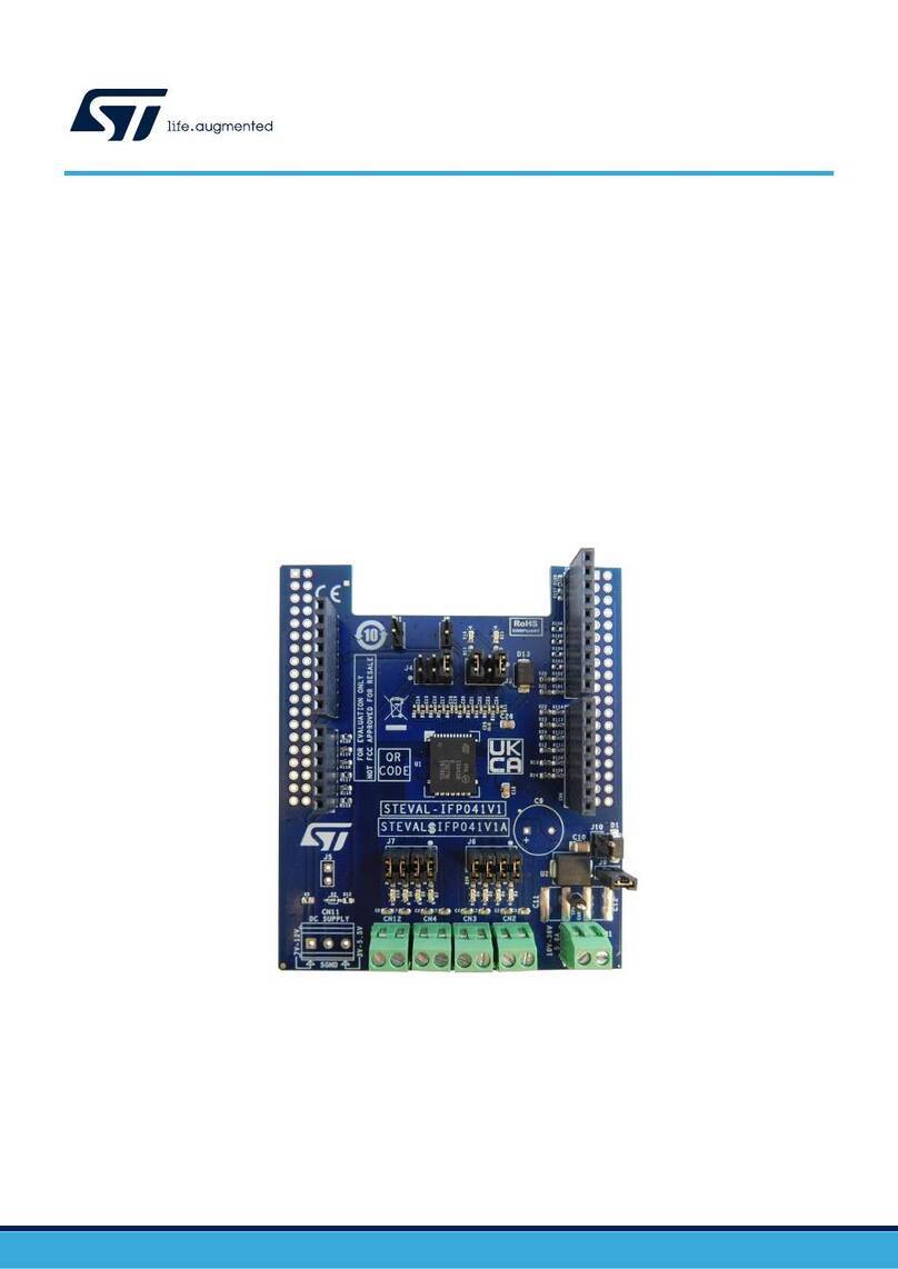
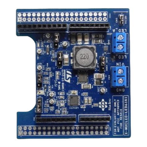
The X-NUCLEO-OUT08A1 industrial digital output expansion board for STM32 Nucleo provides a powerful and flexible
evaluation and development environment for 2 A (typ.) digital output modules, featuring the safe driving and smart diagnostic
capabilities of the IPS160HF single high-side switch.
The X-NUCLEO-OUT08A1 interfaces with the microcontroller on the STM32 Nucleo via 3 kV optocouplers driven by GPIO pins
and Arduino™ UNO R3 (default configuration) and ST morpho (optional, not mounted) connectors.
The expansion board should be connected to either a NUCLEO-F401RE or NUCLEO-G431RB development board, and can
also be stacked with another X-NUCLEO-OUT08A1 or X-NUCLEO-OUT10A1.
Two X-NUCLEO-OUT08A1 expansion boards allows you to evaluate a dual channel digital output module with 2 A (typ.)
capability each, or a 2 A (typ.) single channel safety digital output module. In the second scenario, the first shield output is
connected to the supply of the second one. Dedicated on-board hardware can be enabled or disabled to activate fast discharge
of high capacitive loads, output voltage sensing and additional surge pulse output line protection.
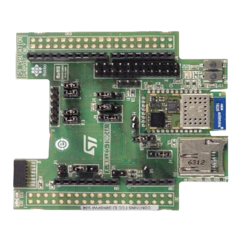
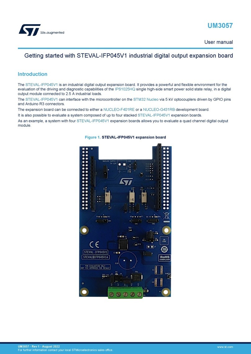
Figure 1. X-NUCLEO-OUT08A1 expansion board
Getting started with X-NUCLEO-OUT08A1 industrial digital output expansion
board for STM32Nucleo
UM2715
User manual
UM2715 - Rev 1 - June 2020
For further information contact your local STMicroelectronics sales office.
www.st.com

1Getting started
1.1 Overview
The X-NUCLEO-OUT08A1 industrial digital output expansion board, embedding the IPS160HF intelligent power
switch (IPS), is designed to meet the application requirement in terms of galvanic isolation between user interface
(or logic side) and power interface (or process side).
This requirement is satisfied by an optical isolation implemented through two couples of optocouplers:
1. The first couple includes:
a. ISO1: for signal forwarding to the device
and
b. ISO2: for diagnostic signal (DIAG pin) feedback
2. The second couple incudes:
a. ISO3: for the additional output voltage feedback signal
and
b. ISO4: for the additional circuitry driving Q1 to allow fast discharge of the output rail
The main features of the X-NUCLEO-OUT08A1 expansion board are:
• Based on IPS160HF single high-side switch, which features:
– Operation up to 60 V/2.4 A
– Low power dissipation (RON(MAX) = 120 mΩ)
– Fast decay for inductive loads
– Open load detection and diagnostics
– Overload and overheating protections with thermal shut-down and cut-off
– PowerSSO-12L package
• Application board operating range: 12 to 33 V/0 to 2.4 A
• Extended voltage operating range (J1 open) up to 60 V
• Status and diagnostic LEDs
• 3 kV galvanic isolation
• Supply rail reverse polarity protection
• Ready for Safety Digital Output Architecture
• EMC compliance with IEC61000-4-2, IEC61000-4-3, IEC61000-4-5
• Wide application development potential in STM32 Nucleo development environment
• Equipped with Arduino™ UNO R3 connectors
• CE certified
• RoHS and China RoHS compliant
1.1.1 Digital section
The digital section is associated with the STM32 interface and digital supply voltage to and from the X-NUCLEO-
OUT08A1 expansion board.
The digital and power sections are isolated by 3.3 mm creepage. Communication between the two sections is
guaranteed by ISO1, ISO2, ISO3 and ISO4 optocouplers.
UM2715
Getting started
UM2715 - Rev 1 page 2/15

Figure 2. X-NUCLEO-OUT08A1 expansion board: digital interface components
The four Arduino® UNO R3 connectors:
• allow expansion board communication with the STM32 Nucleo development board accessing STM32
peripheral and GPIO resources;
• provide digital supply voltage between the STM32 Nucleo development board and the X-NUCLEO-
OUT08A1 expansion board, in either direction.
Normally, the STM32 Nucleo development board supplies the expansion board by 3v3 or 5v0 (JP5 pins 1-2
closed) generated by the USB. You can select the preferred voltage on the expansion board via SW2 (3v3 by
closing pins 1-2; 5v0 by closing pins 2-3).
Alternatively, it is possible to supply the STM32 Nucleo development board by the expansion board. In this case,
an external supply voltage (7-12 V) should be connected to CN2 connector (not mounted by default) on the
expansion board and the ground loop should be closed by mounting D2 (that enables reverse polarity protection)
or by closing J3 (without reverse polarity).
To supply the VIN voltage rail is necessary to:
• close jumper JP5 between pins 2 and 3 and open jumper JP1 on the NUCLEO-F401RE
• open jumper JP5 between pins 1 and 2 and close jumper JP5 between pins 3 and 4 on the NUCLEO-
G431RB
1.1.2 Power section
The power section involves the power supply voltage (CN1, pin 1 VCC, pin 2 GND), load connection (between
CN1 pin 3 and CN1 pin 2) and electromagnetic compatibility (EMC) protection (U2).
UM2715
Overview
UM2715 - Rev 1 page 3/15

Figure 3. X-NUCLEO-OUT08A1 expansion board: power stage components
For EMC:
• the transient voltage suppressor (U2), enabled by closing J1, is placed between VCC and GND tracks to
protect the IPS160HF against surge discharge on the supply rail path up to ±1 kV/2Ω coupling;
• in common mode surge testing, two single-layer capacitors (C1 and C2 - not included) must be soledered at
the predisposed locations;
• the IPS160HF output stages do not require additional EMC protections with respect to IEC61000-4-2 (± 10
kV contact, ±16 kV air), IEC61000-4-4 (± 4 kV), IEC61000-4-5 (± 3.5 kV) standards.
1.2 Hardware requirements
The X-NUCLEO-OUT08A1 expansion board is designed to be used with the NUCLEO-F401RE or NUCLEO-
G431RB STM32 Nucleo development boards.
To function correctly, the X-NUCLEO-OUT08A1 must be plugged onto the matching Arduino® UNO R3 connector
pins on the STM32 Nucleo board as shown below.
UM2715
Hardware requirements
UM2715 - Rev 1 page 4/15

Figure 4. X-NUCLEO-OUT08A1 and STM32 Nucleo stack
1.3 System requirements
To use the STM32 Nucleo development boards with the X-NUCLEO-OUT08A1 expansion board, you need:
• a Windows PC/laptop (Windows 7 or above)
• a type A to mini-B USB cable to connect the STM32 Nucleo board to the PC when using a NUCLEO-
F401RE development board
• a type A to micro-B USB cable to connect the STM32 Nucleo board to the PC when using a NUCLEO-
G431RB development board
• the X-CUBE-OUT8 firmware and software package installed on your PC/laptop
1.4 Board setup
Step 1. Connect the X-NUCLEO-OUT08A1 to the NUCLEO-F401RE or NUCLEO-G431RB development board
through the Arduino connectors.
Step 2. Connect the X-NUCLEO-OUT08A1 power section (see Section 1.1.2 Power section).
Step 3. Connect the load between CN1 pins 2 and 3.
Step 4. Connect the mini-USB (for NUCLEO-F401RE) or micro-USB (for NUCLEO-G431RB) cable between
your PC and the STM32 Nucleo board.
Step 5. Download the selected firmware (STSW-OUT8F4 for NUCLEO-F401RE or STSW-OUT8G4 for
NUCLEO-G431RB) onto the microcontroller.
Step 6. Provide the digital supply voltage (see Section 1.1.1 Digital section).
Step 7. Reset the example sequence by pushing the black button on the STM32 Nucleo board.
UM2715
System requirements
UM2715 - Rev 1 page 5/15

Step 8. Push the blue button on STM32 Nucleo board to choose among the examples provided in the default
firmware package.
Note: When using two boards stacked (e.g. dual channel digital output or single channel safety digital output
application), you have to move some signal enabler resistors from DEFAULT to ALTERNATE position. You can
refer to the expansion board schematic and/or to the table below (where board 0 mounts all the resistors in their
DEFAULT position).
Table 1. Pin position when using a board stack
Board 0 Board 1
IN1 Nch_DRV DIAG OUT_FB IN1 Nch_DRV DIAG OUT_FB
R101 R102 R103 R104 R111 R134 R112 R131
UM2715
Board setup
UM2715 - Rev 1 page 6/15

2Schematic diagrams
Figure 5. X-NUCLEO-OUT08A1 circuit schematic (1 of 2)
J1
5
27
16
IN1
36
1
2
DIAG
R121 100 (N.M.)
1
1
R125 100 (N.M.)
16
Arduino Connectors
OUT_FB
PA9
2
17
OUT1
Nch-DRV
11
6
R101 100
6
J3
4
Nch-DRV
20
3
12
8
38
2
214
31
19
109
CN5
SSQ-110-04-F-S
Alternate Nucleo Supply
7V - 12 V
+
3
DIAG
1
23
3
18
5
22
8
5
1
35
17
Not Assembly
OUT_FB
7
3
PB5
PC7
21
31
ALTERNATE USE
R124 100 (N.M.)
13
9
2
PB0
PC0
PA5
24
2
34
R104 100
Nch-DRV
4
13
6
CN9
SSQ-108-04-F-S
3V3
J2
R133 100 (N.M.)
Nch-DRV
7
R111 100 (N.M.)
Analog supply
8V - 60 V
OUT_FB
33
VIN
R103 100
C3
2.2uF
PA1
PB4
PA3
8
ALTERNATE USE
4
5
OUT_FB
R102 100
21
TP9
5001
24
4
OUT_FB
26
DIAG R112 100 (N.M.)
20
R123 100 (N.M.)
IN1
OUT_FB
DIAG
2
7
5
default open
VIN
EARTH
D2 BAT48 (N.M.)
IN1
25
ALTERNATE USE
ALTERNATE USE
DEFAULT
ALTERNATE USE
ALTERNATE USE
ALTERNATE USE
ALTERNATE USE
ALTERNATE USE
3
Nch-DRV
4
2
19
35
IN1
10
30
38
C8
47uF (N.M.)
DIAG
26
28
4
10
5V
6
CN7
SSQ-119-04-L-D (N.M.)
2
8
22
DEFAULT
DEFAULT
ALTERNATE USE
36
1
32
7
12
DIAG
TP8
5001
IN1
ALTERNATE USE
Nch-DRV
3v3
30
7
CN6
SSQ-108-04-F-S
18
32
C1
4700pF
3
6
1
STPS1H100A
37
3
15
9
VCC
GND
U2
SM15T39CA
2
1
OUT1
6
PA7
PC1
15
ALTERNATE USE
29
5v0
AVDD
IOREF
R122 100 (N.M.)
33
Morpho Connectors
(N.M.)
R131 100 (N.M.) IN1
default closed
default open
5
CN2
Con2
14
25
R130 100 (N.M.)
28
C2
4700pF
34
R132 100 (N.M.)
37
CN1
Con3
PB8
PA10
PA4
PA2
PB9
PA0
PB10
CN8
SSQ-106-04-F-S
29
8
PA8
PA6
PB6
(7V-12V NUCLEO supply voltage)
R134 100 (N.M.)
VCC
11
27
23
1
1
U3
ESDA15P60-1U1M (N.M.)
CN10
SSQ-119-04-L-D (N.M.)
NRST
D1
PB3
DEFAULT
UM2715 - Rev 1 page 7/15
UM2715
Schematic diagrams

Figure 6. X-NUCLEO-OUT08A1 circuit schematic (2 of 2)
NC1
5
3DIAG
12
VCC
13
1
3v3
ANY
R3
R15
TP7
STPS1H100A
2
R13
27K
con8-2x4-strip-male
4
10nF
default closed
(open load detection = active)
con8-2x4-strip-male
2
8
2
2
R4
1
3
2.2K
ANY
ACPL-217-50AE
R11
2
R2
1
Vcc_TAB
OUT1
J7
TR3
27K
3
con3-strip-male
2
Nch-DRV
100nF
R96.8k
VCC
TP3
2
OUT2
OUT3 10
C6
22k
7
3
8
SW2
2.2K
J14
8
OUT1
D7
Q1
0.1uF
R14
C
3
27K
ACPL-217-50AE
9
ISO2
1Vcc1
C5
IPS160HF
VCC
5001
J13
1
1
4
68k
CoD
4
390
1
J9
GND 7
OUT4 11
5001
4
ACPL-217-50AE
1k
3
IN
2
ISO4
1
4
ISO3
6
1k
C7
47nF
2
SW1
con3-strip-male
U1
1
J8
D8
BAT41ZFILM
TP6
3
A
RED
C
Vcc2
5
4
3
R6
1.5k
D6
NC2
6
2.2K
R12
R16
TDZ6V2J,115
R7
SM15T10AY
1
STN2NF10
DIAG
R5
R10
6.8k
J5
OUT1
5v0
6
5001
R8
J4
default: closed
default:
close 1-2
default:
closed
default:
CLOSE 2-3
default:
3-4 = CLOSE
default:
1-2, 5-6, 7-8 = OPEN
closed
default:
open
default:
3-4 = CLOSE
2
D5
R1
150060VS75000
4
3
A
ACPL-217-50AE
IN1
ISO1
1-2, 5-6, 7-8 = OPEN
D3
22k
OUT_FB
390
5
7
3
C4
UM2715 - Rev 1 page 8/15
UM2715
Schematic diagrams

3Bill of materials
Table 2. X-NUCLEO-OUT08A1 bill of materials
Item Q.ty Ref. Part/Value Description Manufacturer Order code
1 2 C1, C2 4700 pF Capacitors Vishay Vitramon HV1825Y472KXHATHV
2 1 C3 2.2 µF Capacitor AVX 12061C225KAT2A
3 1 C4 100 nF Capacitor Wurth Electronics
Inc. 885012207128
4 1 C5 10 nF Capacitor Murata Electronics
North America GRM188R71H103KA01D
5 1 C6 47 nF Capacitor Murata Electronics
North America GCM188R71H473KA55D
6 1 C7 0.1 µF Capacitor Kemet C0603C104K5RACTU
7 1 C8 47 µF Capacitor Wurth Electronics
Inc. 860040875002
8 1 CN1 Con3 Fixed terminal
block
Wurth Electronics
Inc. 691214110003
9 1 CN2 Con2 Fixed terminal
block
Wurth Electronics
Inc. 691214110002
10 1 CN5 SSQ-110-04-F-S Connector Samtec Inc. SSQ-110-04-F-S
11 2 CN6, CN9 SSQ-108-04-F-S Connectors Samtec Inc. SSQ-108-04-F-S
12 2 CN7, CN10 SSQ-119-04-L-D
(N.M.) Connectors Samtec Inc. SSQ-119-04-L-D
13 1 CN8 SSQ-106-04-F-S Connector Samtec Inc. SSQ-106-04-F-S
14 2 D1, D7 STPS1H100A 100 V, 1 A power
Schottky rectifier ST STPS1H100A
15 1 D2 BAT48 (N.M.)
40 V, 350 mA axial
general purpose
signal Schottky
diode
ST BAT48JFILM
16 1 D3 BAT41ZFILM
100 V, 200 mA
surface mount
general purpose
signal Schottky
diode
ST BAT41ZFILM
17 1 D5 150060RS75000 LED Wurth Electronics
Inc. 150060RS75000
18 1 D6 150060VS75000 LED Wurth Electronics
Inc. 150060VS75000
19 1 D8 TDZ6V2,J115 Zener diode Nexperia USA Inc. TDZ6V2,J115
20 4 ISO1 ISO2 ISO3
ISO4 ACPL-217-50AE Optocouplers Broadcom Ltd. ACPL-217-50AE
21 8 J1, J2, J3, J4, J5,
J7, J8, J9
Strip 2x1 pitch
2.54 mm., con2-
strip-male
Jumpers Sullins Connector
Solutions STC02SYAN
22 2 J13, J14
con8-2x4-strip-
male pitch 2.54
mm
Connectors Amphenol ICC 67996-408HLF
UM2715
Bill of materials
UM2715 - Rev 1 page 9/15

Item Q.ty Ref. Part/Value Description Manufacturer Order code
23 1 Q1 STN2NF10
N-channel 100 V,
0.23 Ohm, 2.4 A
STripFET(TM) II
power MOSFET
ST STN2NF10
24 2 R1, R2 27 K Resistors Yageo RC0603FR-0727KL
25 2 R3, R4 2.2 K Resistors Yageo RC0603FR-072K2L
26 2 R5, R6 390 Resistors Yageo RC0603FR-07390RL
27 2 R7, R8 15 k Resistors Yageo RC0603FR-0715KL
28 2 R9 R10 6.8 k Resistors Yageo RC0603FR-076K8L
29 1 R11 1 k Resistor Yageo RC0603FR-071KL
30 3 R12, R13, R14 22 k Resistors Yageo RC0603FR-0722KL
1 R15 68 k Resistor Yageo RC0603FR-0768KL
32 1 R16 10 k Resistor Yageo RC0603FR-0710KL
33 4 R101, R102,
R103, R104 100 k Resistors Yageo RC0603FR-07100RP
34 12
R111, R112,
R121, R122,
R123, R124,
R125, R130,
R131, R132,
R133, R134
100 k (N.M.) Resistors Yageo RC0603FR-07100RP
35 2 SW1, SW2 con3-strip-male Switches Any Any
36 5 TP3, TP6, TP7,
TP8, TP9 5001 Test points Keystone
Electronics 5001
37 1 TR3 SM15T10AY Automotive 1500
W TVS in SMC ST SM15T10AY
38 1 U1 IPS160HF Single high-side
switch ST IPS160HF
39 1 U2 SM15T39CA 1500 W, TVS in
SMC ST SM15T39CA
40 1 U3 ESDA15P60-1U1
M (N.M.)
High-power
transient voltage
suppressor (TVS)
ST ESDA15P60-1U1M
UM2715
Bill of materials
UM2715 - Rev 1 page 10/15

Revision history
Table 3. Document revision history
Date Revision Changes
12-Jun-2020 1 Initial release.
UM2715
UM2715 - Rev 1 page 11/15

Contents
1Getting started ....................................................................2
1.1 Overview .....................................................................2
1.1.1 Digital section ...........................................................2
1.1.2 Power section ...........................................................3
1.2 Hardware requirements .........................................................4
1.3 System requirements ...........................................................5
1.4 Board setup ...................................................................5
2Schematic diagrams ...............................................................7
3Bill of materials....................................................................9
Revision history .......................................................................11
UM2715
Contents
UM2715 - Rev 1 page 12/15

List of tables
Table 1. Pin position when using a board stack .....................................................6
Table 2. X-NUCLEO-OUT08A1 bill of materials .....................................................9
Table 3. Document revision history ............................................................. 11
UM2715
List of tables
UM2715 - Rev 1 page 13/15

List of figures
Figure 1. X-NUCLEO-OUT08A1 expansion board...................................................1
Figure 2. X-NUCLEO-OUT08A1 expansion board: digital interface components ..............................3
Figure 3. X-NUCLEO-OUT08A1 expansion board: power stage components ................................4
Figure 4. X-NUCLEO-OUT08A1 and STM32 Nucleo stack.............................................5
Figure 5. X-NUCLEO-OUT08A1 circuit schematic (1 of 2) .............................................7
Figure 6. X-NUCLEO-OUT08A1 circuit schematic (2 of 2) .............................................8
UM2715
List of figures
UM2715 - Rev 1 page 14/15

IMPORTANT NOTICE – PLEASE READ CAREFULLY
STMicroelectronics NV and its subsidiaries (“ST”) reserve the right to make changes, corrections, enhancements, modifications, and improvements to ST
products and/or to this document at any time without notice. Purchasers should obtain the latest relevant information on ST products before placing orders. ST
products are sold pursuant to ST’s terms and conditions of sale in place at the time of order acknowledgement.
Purchasers are solely responsible for the choice, selection, and use of ST products and ST assumes no liability for application assistance or the design of
Purchasers’ products.
No license, express or implied, to any intellectual property right is granted by ST herein.
Resale of ST products with provisions different from the information set forth herein shall void any warranty granted by ST for such product.
ST and the ST logo are trademarks of ST. For additional information about ST trademarks, please refer to www.st.com/trademarks. All other product or service
names are the property of their respective owners.
Information in this document supersedes and replaces information previously supplied in any prior versions of this document.
© 2020 STMicroelectronics – All rights reserved
UM2715
UM2715 - Rev 1 page 15/15
Table of contents
Other ST Computer Hardware manuals

ST
ST STM32 Nucleo User manual

ST
ST UM2033 User manual

ST
ST STM32F10 Series Installation and operating instructions

ST
ST STDES-65ACFADP Specification sheet

ST
ST ST7-EMU3 Series User manual

ST
ST STEVAL-BCN002V1B User manual

ST
ST STEVAL-IHM017V1 User manual

ST
ST STM32F4 Series Owner's manual

ST
ST ST25DV-DISCOVERY User manual

ST
ST X-NUCLEO-6283A1 User manual

ST
ST STM32F4 Series User manual

ST
ST UM2168 User manual

ST
ST STM32G0 User manual

ST
ST X-NUCLEO-IDW04A1 User manual
ST
ST X-NUCLEO-IHM09M1 User manual

ST
ST X-NUCLEO-DRP1M1 User manual

ST
ST X-NUCLEO-OUT06A1 User manual

ST
ST ControlBD-7FMC2 User manual

ST
ST STEVAL-ST25R3916B User manual

ST
ST STEVAL-ISF001V2 User manual