ST X-NUCLEO-OUT17A1 User manual

Introduction
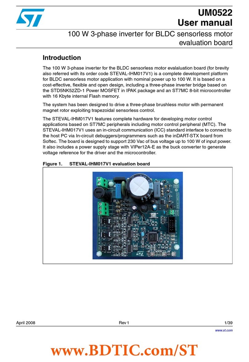
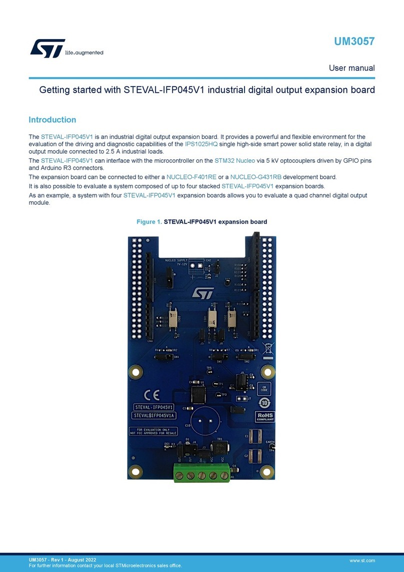
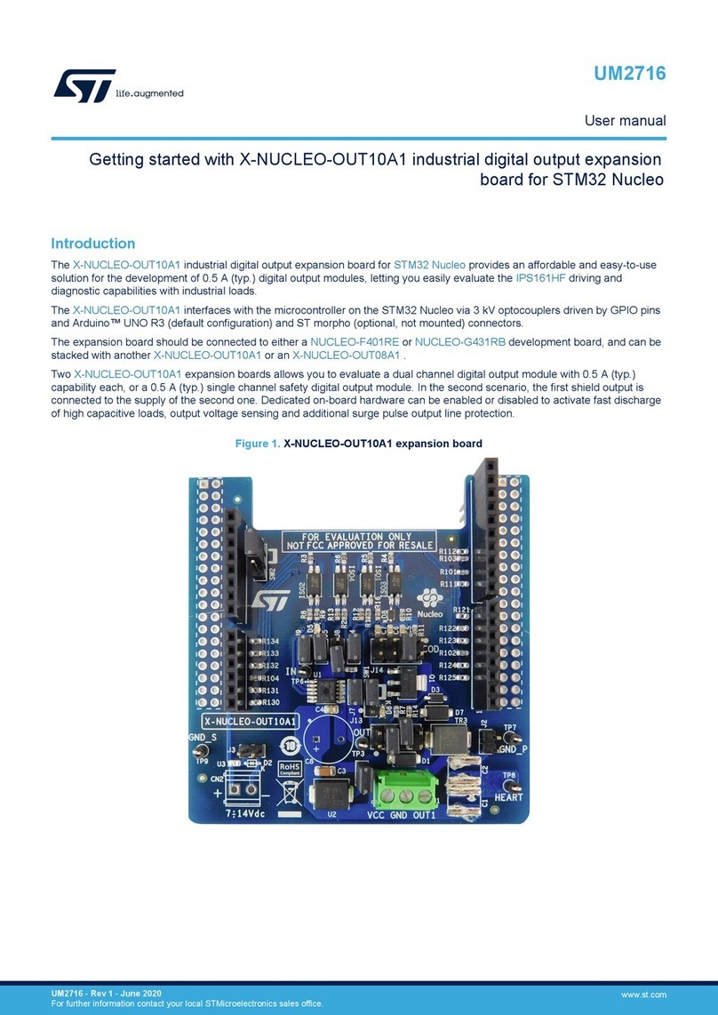
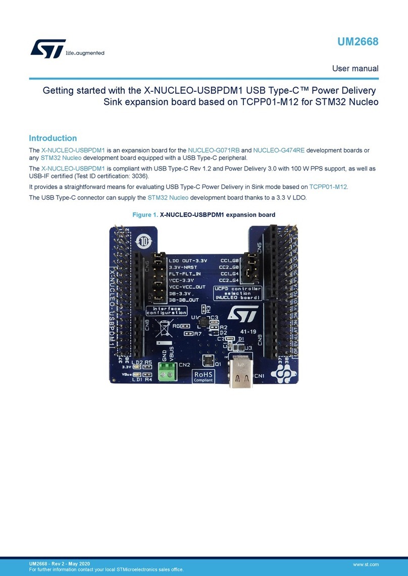
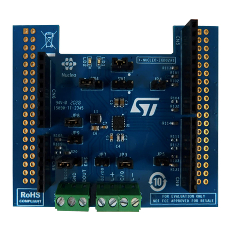
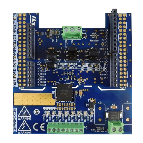
The X-NUCLEO-OUT17A1 is an industrial digital output expansion board for STM32 Nucleo. It provides a powerful and flexible
environment for the evaluation of the driving and diagnostic capabilities of the IPS8200HQ-1 octal high-side, smart power, solid-
state relay in a digital output module connected to 1.0 A industrial loads.
The X-NUCLEO-OUT17A1 interfaces with the microcontroller on the STM32 Nucleo via STISO620 and STISO621 and
Arduino® UNO R3 connectors.
The user can select which driving mode controls the IPS8200HQ-1: parallel (SEL2 = L by JP21 = open) or SPI (SEL2 = H by
JP21 = closed).
In the case of SPI selection, the user can select the communication protocol between 8 bits (SEL1 = L by JP22 = open) or 16
bits (SEL1 = H by JP22 = closed).
The VCC supply pin of the IPS8200HQ-1 is provided by the connector CN1, while the loads (driven by the 8 output channels of
the IPS8200HQ-1) can be connected between the connectors CN2, CN3, CN4, CN12, and the pin 2 of the connector CN1.
The on-board digital isolators (STISO620 and STISO621) feature the 2.8k VRMS (4k VPK) galvanic isolation between the two
application sides: logic and process sides.
The logic side is the application side of the MCU and it is supplied by the VISO_L rail (3.3 or 5.0 V). VISO_L can be supplied by
an external power supply connected to CN13 or, alternatively by the pin 4 (SW1 = close 1-2) or pin 5 (SW1 = close 2-3) of CN6.
The process side is the application side of the industrial loads and it is supplied by the VCC and VISO_P rails. The VISO_P (3.3
or 5.0 V) is usually supplied by the VREG rail (JP31 = closed) that can be generated by the step-down embedded in the
IPS8200HQ-1 (SW17 = close 1-2, JP20 = closed, JP15 = closed and JP28 = close 2-4 (VREG = 3.3 V) or JP28 = 1-3 (VREG =
5.0 V)).
Alternatively, VREG can be provided by an external power supply connected to CN14 (SW17 = close 2-3, JP20 = open, JP15 =
open).
In parallel driving mode (active with the default jumper and switch settings) the application board can work even without any
Nucleo board: in this case, the user must provide the process side voltage (usually 24 V) by the CN1 and the VISO_L (usually
3.3 V) by the CN13. The INX signals, available on CN5[1, 2, 3], CN8[4] and CN9[3, 5, 7, 8], drives on/off the correspondent
OUTX connected to the loads on the process side.
The INX pins can be driven low/high swinging between 0V and VISO_L. The activation of each OUTX (OUT1… OUT8) can be
monitored by the green LEDs DOX (DO1… DO8).
The activation of the three diagnostic pins (TWARN, PGOOD, FAULT) can be visualized on the correspondent red LEDs (D11,
D12, D13, respectively) or monitored by an oscilloscope on CN8[5], CN5[9], CN5[10].
The SPI driving mode can be set by changing the default configuration (JP21 = close; SW4, SW5, SW6, SW7, SW9, SW10,
SW11, SW12, SW13, SW14, SW15 and SW20 = close 2-3, SW18 = close 1-2). The SPI-8bits is the default mode (JP22 =
open), while the SPI-16bits mode can be activated by JP22 = close.
In SPI driving mode it is also possible to activate the MCU freeze detection feature by setting SW3 = close 2-3.
The expansion board can be connected to either a NUCLEO-F401RE or a NUCLEO-G431RB development board. In this case
the companion firmware X-CUBE-IPS detects the selected configuration (GPIO, SPI-8bits, SPI-16bits) by reading the signals
SEL2_L and SEL1 from CN8[1] and CN8[6]. The activation of the MCU freeze feature is detected by WDEN(in) on CN9[4].
It is also possible to evaluate a system composed of a X-NUCLEO-OUT17A1 stacked on other expansion boards. In fact, SPI
driving mode allows the daisy-chaining communication with another X-NUCLEO-OUT17A1 stacked through the Arduino
connectors: the two stacked boards must be configured with SW6, SW18 = close 2-3 on one board, and SW6, SW18 = close
1-2 on the other board.
Getting started with the X-NUCLEO-OUT17A1 industrial digital output expansion
board for STM32 Nucleo
UM3247
User manual
UM3247 - Rev 1 - November 2023
For further information contact your local STMicroelectronics sales office. www.st.com
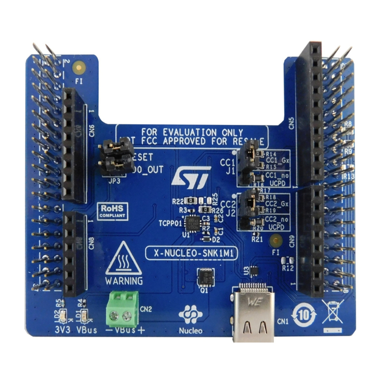
Figure 1. X-NUCLEO-OUT17A1 expansion board
UM3247
UM3247 - Rev 1 page 2/25

1 Getting started
1.1 Overview
The X-NUCLEO-OUT17A1 embeds the IPS8200HQ-1 intelligent power switch (IPS), which features serial/parallel
selectable interface on-chip, 8-bit and 16-bit SPI interface for IC command and control diagnostic, Power Good
diagnostic, IC warning temperature detection, overcurrent and overtemperature protection for safe output loads
control.
The board is designed to meet the application requirements for the galvanic isolation between the user and power
interfaces.
An optical isolation satisfies this requirement. The isolation is implemented through three dual channel digital
isolators with 2 – 0 channel directionality (U3, U11, U12) for the input signals forward to the device, and four dual
channel digital isolators with 1 – 1 channel directionality (U4, U6, U7, U10) for the diagnostic feedback signals of
the device and the daisy chaining service lines.
The expansion board features:
• Based on the IPS8200HQ-1 octal high-side switch, which features:
– Operating range 10.5 to 36 V
– Operating output current ≤ 1.0 A
– Low power dissipation (RON(MAX) = 200 mΩ)
– Undervoltage lock-out
– Selectable driving modes parallel or 5 MHz SPI (8 or 16 bits)
– Embedded step-down converter
– 4x2 LED matrix for efficient status indication
– MCU freeze detection
– Fast decay for inductive loads
– Overload and overtemperature protections
– Loss of ground protection
– Junction Overtemperature and parity check diagnostic pin (FAULT)
– Case overtemperature diagnostic pin (TWARN)
– Supply voltage Level diagnostic pin (PGOOD)
– QFN48L 8x6 mm package
• Application board voltage operating range: 12 to 33 V
• Extended voltage operating range (J9 open) up to 36 V
• Operating current: up to 1.0 A per channel
• Blue LED showing SPI mode selection
• Yellow LED showing SPI mode 16-bits selection
• Red LED for FAULT diagnostic pin (JP12 closed)
• Red LED for PGOOD diagnostic pin (JP13 closed)
• Red LED for TWARN diagnostic pin (JP27 closed)
• 4 kVPK galvanic isolation guaranteed by STISO620 and STISO621
• Supply rail reverse polarity protection
• Compatible with STM32 Nucleo development boards
• Equipped with Arduino® UNO R3 connectors
• RoHS and China RoHS compliant
• CE certified
UM3247
Getting started
UM3247 - Rev 1 page 3/25

1.2 Board configuration
A set of jumpers and switches is available to configure the board. Table 1 shows the configurations to be used
respectively for Parallel 8 Channels Mode, SPI 8 Channels Mode and Daisy Chain Mode.
Table 1. X-NUCLEO-OUT17A1
Jumpers/Switches Parallel 8 Ch SPI 8 Ch Daisy Chain
SW1, SW3, SW17 Closed 1-2 Closed 1-2 Closed 1-2
JP1, JP2, JP3, JP4, JP5, JP6, JP7,
JP8, JP9, JP12, JP13, JP15, JP20,
JP23, JP24, JP25, JP27, JP31
Closed Closed Closed
JP10, JP14, JP16, JP17, JP18, JP19 Open Open Open
JP11 Not mounted Not mounted Not mounted
JP28 Closed 2-4 Closed 2-4 Closed 2-4
JP29, JP30 Closed 1-2, 3-4, 5-6,
7-8 Closed 1-2, 3-4, 5-6, 7-8 Closed 1-2, 3-4, 5-6, 7-8
SW4, SW5, SW7, SW9, SW10,
SW11, SW12, SW13, SW14, SW15 Closed 1-2 Closed 2-3 Board 0: Closed 2-3
Board 1: Closed 1-2
SW6 Closed 1-2 Closed 2-3 Board 0: Closed 2-3
Board 1: Closed 1-2
SW18 Open Closed 1-2 Board 0: Closed 2-3
Board 1: Closed 1-2
SW20 Closed 1-2 Closed 2-3 Closed 2-3
JP21 Open Closed Closed
JP22 Open Open (SEL1 L, SPI 8bits)
Closed (SEL1 H, SPI 16 bits)
Open (SEL1 L, SPI 8bits)
Closed (SEL1 H, SPI 16 bits)
UM3247
Board configuration
UM3247 - Rev 1 page 4/25

1.3 Digital section
The digital section is associated with the STM32 interface and the digital supply voltage to and from the X-
NUCLEO-OUT17A1 expansion board.
Figure 2. X-NUCLEO-OUT17A1 expansion board: digital interface section
The dotted green line indicates the whole digital interface section. The pink rectangles identify the Arduino® UNO
R3 connectors and the yellow ones identify STISO620 and STISO621 digital isolators.
The four Arduino® UNO R3 connectors:
• allow the expansion board to communicate with the STM32 Nucleo development microcontroller board
accessing the STM32 peripheral and GPIO resources;
• provide the digital supply voltage between the STM32 Nucleo development board and the X-NUCLEO-
OUT17A1 expansion board, in either direction.
The five digital isolators (STISO620 and STISO621) provide 4 kVPK galvanic isolation between logic and process
sides of the expansion board.
Usually, the STM32 Nucleo development board supplies the expansion board by a 3.3 V or 5.0 V generated by
the USB.
Alternatively, it is possible to supply the STM32 Nucleo development board from the expansion board. In this
case, an external supply voltage (7-12 V) should be connected to the CN11 connector (not mounted by default)
on the expansion board and the ground loop should be closed by mounting D2 (enabling the reverse polarity
protection) or by closing JP11 (without reverse polarity).
To supply the VIN voltage rail, it is necessary to:
UM3247
Digital section
UM3247 - Rev 1 page 5/25

• close the JP5 jumper between pins 2 and 3 and open the JP1 jumper on the NUCLEO-F401RE;
• open the JP5 jumper between pins 1 and 2 and close the JP5 jumper between pins 3 and 4 on the
NUCLEO-G431RB.
Logic side is then supplied by the VISO_L rail (3.3 V or 5.0 V). VISO_L can be supplied by an external power
supply connected to CN13 (SW1 open) or, alternatively by the pin 4 (SW1 = close 1-2) or pin 5 (SW1 = close 2-3)
of CN6.
The user can select which driving mode controls the IPS8200HQ-1: parallel (SEL2 = L by JP21 = open) or SPI
(SEL2 = H by JP21 = closed). In the case of SPI selection, the user can select the communication protocol
between 8 bits (SEL1 = L by JP22 = open) or 16 bits (SEL1 = H by JP22 = closed).
UM3247
Digital section
UM3247 - Rev 1 page 6/25

1.4 Power section
The power section involves the power supply voltage (CN1, pin 1 for VCC, pin 2 for GND), the load connection
(eight loads can be connected between each pin of CN2, CN3, CN4, and CN12 and pin 2 of CN1), EMC
protections (U2), and supply reverse polarity protection (D1).
Figure 3. X-NUCLEO-OUT17A1 expansion board: power section
1. IPS8200HQ-1
2. Output and power supply connector
3. Output channels - green LEDs
4. FAULT (diagnostic pin) red LED
5. PGOOD (diagnostic pin) red LED
6. TWARN (diagnostic pin) red LED
7. SEL2 H (SPI) blue LED
8. SEL1 H (16 bits SPI data width) yellow LED
The process side is supplied by the VCC and VISO_P rails. The VISO_P (3.3 or 5.0 V) is usually supplied by the
VREG rail (JP31 = closed) that can be generated by the step-down embedded in the IPS8200HQ-1 (SW17 =
close 1-2, JP20 = closed, JP15 = closed and JP28 = close 2-4 (VREG = 3.3 V) or JP28 = 1-3 (VREG = 5.0 V)).
Alternatively, VREG can be provided by an external power supply connected to CN14 (SW17 = close 2-3, JP20 =
open, JP15 = open).
For EMC:
• the SMC30J30CA transient voltage suppressor (U2), enabled by closing J9, is placed between VCC and
GND tracks to protect the IPS8200HQ-1 against surge discharge on the supply rail path up to ±1 kV/2 Ω
coupling;
UM3247
Power section
UM3247 - Rev 1 page 7/25

• in the common mode surge testing, two single-layer capacitors (C11 and C12 - not included) must be
soldered at the predisposed locations;
• the IPS8200HQ-1 output stages do not require additional EMC protections with respect to the
IEC61000-4-2, IEC61000-4-3, IEC61000-4-4, IEC61000-4-5, IEC61000-4-8 standards.
The EMC performance of the X-NUCLEO-OUT17A1 is detailed below:
• for emission (when the DC input port of the board is powered by an AC-DC, DC-DC or battery with a cable
that does not exceed a three-meter length), compliance with standards:
– EN IEC 61000-6-3:2021
– EN 55032:2015 +A1:2020
• for immunity, compliance with standards:
– EN IEC 61000-6-1:2019
– EN 55035:2017 +A11:2020
UM3247
Power section
UM3247 - Rev 1 page 8/25

1.5 Hardware requirements
The X-NUCLEO-OUT17A1 expansion board is designed to be used with the NUCLEO-F401RE or NUCLEO-
G431RB STM32 Nucleo development boards.
To function correctly, the X-NUCLEO-OUT17A1 must be plugged onto the matching Arduino® UNO R3 connector
pins on the STM32 Nucleo board as shown below.
Figure 4. X-NUCLEO-OUT17A1 and STM32 Nucleo stack
1.6 System requirements
To use the STM32 Nucleo development boards with the X-NUCLEO-OUT17A1 expansion board, you need:
• a Windows PC/laptop (Windows 7 or above)
• a type A to mini-B USB cable to connect the STM32 Nucleo board to the PC when using a NUCLEO-
F401RE development board
• a type A to micro-B USB cable to connect the STM32 Nucleo board to the PC when using a NUCLEO-
G431RB development board
• the X-CUBE-IPS firmware and software package installed on your PC/laptop
UM3247
Hardware requirements
UM3247 - Rev 1 page 9/25

1.7 Board setup
Step 1. Connect the mini-USB or micro-USB cable to your PC to use the X-NUCLEO-OUT17A1 with NUCLEO-
F401RE or NUCLEO-G431RB development board
Step 2. Download the proper firmware (.bin) onto the STM32 Nucleo development board microcontroller
through STM32 ST-LINK utility, STM32CubeProgrammer, and according with the information detailed
in the table below. The X-NUCLEO-OUT17A1 can be used to control the IPS8200HQ-1 device in three
different operating modes available for the user in three different example projects:
Parallel_8_Channels (one board configured in parallel 8 channels mode, direct pin input interface),
SPI_8_Channels (one board configured in SPI 8 channels mode, SPI input interface) and DaisyChain
(two stacked boards properly configured in Daisy chain mode, SPI input interface with daisy chaining).
The binary files provided with the X-CUBE-IPS software package enable the user to choose the
preferred control mode by selecting the binary file contained in the proper example project Binary
folder, as reported in the following table
Table 2. Nucleo development boards binary files
Nucleo board Binary path
NUCLEO-F401RE
Projects\STM32F401RE-Nucleo\Examples\OUT17A1\DaisyChain\Binary\DaisyChain.bin
Projects\STM32F401RE-
Nucleo\Examples\OUT17A1\Parallel_8_Channels\Binary\Parallel_8_Channels.bin
Projects\STM32F401RE-
Nucleo\Examples\OUT17A1\SPI_8_Channels\Binary\SPI_8_Channels.bin
NUCLEO-G431RB
Projects\STM32G431RB-Nucleo\Examples\OUT17A1\DaisyChain\Binary\DaisyChain.bin
Projects\STM32G431RB-
Nucleo\Examples\OUT17A1\Parallel_8_Channels\Binary\Parallel_8_Channels.bin
Projects\STM32G431RB-
Nucleo\Examples\OUT17A1\SPI_8_Channels\Binary\SPI_8_Channels.bin
Note: Additional details on each operating mode configuration are available inside the X-CUBE-IPS
software package as reported in the below table:
Table 3. Additional information on board configuration
Board configuration Readme file
DaisyChain Examples\OUT17A1\DaisyChain\readme.html
Parallel_8_Channels Examples\OUT17A1\Parallel_8_Channels\readme.html
SPI_8_Channels Examples\OUT17A1\SPI_8_Channels\readme.html
Step 3. Connect the IPS8200HQ-1 device supply voltage via CN1 (see Section 1.4 Power section).
Step 4. Provide the digital supply voltage (see Section 1.3 Digital section).
Step 5. Connect the load on the output connector (see Section 1.4 Power section).
Step 6. Reset the example sequence by pushing the black button on the STM32 Nucleo board.
Step 7. Push the blue button on the STM32 Nucleo board to choose among the examples provided in the
default firmware package.
UM3247
Board setup
UM3247 - Rev 1 page 10/25

2 Schematic diagrams
Figure 5. X-NUCLEO-OUT17A1 circuit schematic (1 of 3)
def aul t :
Cl os e 1- 2
PB3
PB5
PA8
PB10
PA10
PA2
PB4
PA3
DEFAULT
Alternate Nucleo supply
7 - 12 V
(7 - 12 V Nucleo supply open)
DEFAULT
def aul t cl osed
Arduino connectors
AVDD
default open
PC7
def aul t open
DEFAULT
PA7
PA6
PB8
DEFAULT
PA5DEFAULT
Analog supply
1 0 - 36 V
I OREF
NRST
PB9
DEFAULT
PB6
DEFAULT
Morpho connectors
(not mounted)
DEFAULT
PA9
External logic side supply
(3.3 or 5.0 V)
DEFAULT
DEFAULT
PC0
DEFAULT
DEFAULT/ Al t er nat e use
DEFAULT
PA4
PC1
DEFAULT
DEFAULT
PB0
DEFAULT
DEFAULT
PA1
PA0
DEFAULT
DEFAULT
VCC
OUT1
OUT2
OUT3
OUT4
OUT5
OUT6
OUT7
OUT8
VISO_L
FAULT_L
IN1 SPI_MISO TWARN_LSEL2_L
IN2/WDEN SPI_MOSI PGOOD_L
IN3 SPI_CLK
SEL1
IN4
OUT_EN
IN5/DAISY_CHAIN
IN6 WD
IN7/SPI_SS
IN8
3v3 5v0
JP10
D18
LED BLUE
AC
R108 100
R119 100
CN8
SSQ-106-04-F-S
1
2
3
4
5
6
R60 220k
SW3
1
2
3
C12
4700pF
N.M.
D19
LED YELLOW
AC
R117 100
R109 100
R105 100
JP16
R110 100
R120 100
JP9
+
C9
47uF
N.M
12
R103 100
CN5
SSQ-110-04-F-S
1
2
3
4
5
6
7
8
9
10
R113 100
CN4
1
2
R21
0
R37 150
R101 100
R36 150
R58 220k
U9
ESDA15P60-1U1M
R111 100
R56 220k
R114 100
C10
2.2uF
CN2
1
2
C49
2.2uF
R52 220k
R54 220k
U5
ESDA15P60-1U1M
N.M
D2
BAT48JFILM
N.M.
CN6
SSQ-108-04-F-S
1
2
3
4
5
6
7
8
C11
4700pF
N.M.
CN12
1
2
R106 100
CN3
1
2
CN10
SSQ-119-04-L-D
N.M.
1 2
3 4
5 6
7 8
9 10
11 12
13 14
15 16
17 18
19 20
21 22
23 24
25 26
27 28
29 30
31 32
33 34
35 36
37 38
R118 100
R104 100
CN9
SSQ-108-04-F-S
1
2
3
4
5
6
7
8
JP11 N.M.
R55 220k
CN7
SSQ-119-04-L-D
N.M.
1 2
3 4
5 6
7 8
9 10
11 12
13 14
15 16
17 18
19 20
21 22
23 24
25 26
27 28
29 30
31 32
33 34
35 36
37 38
D1 STPS1H100A
R51 220k
TP1
5001
R57 220k
R115 100
R102 100
CN11
1
2
R116 100
R107 100
CN13
1
2
D15
BAT48JFILM
R53 220k
CN1
691214110002
1
2
U2
SMC30J30CA
12
EARTH
FAULT_L
PGOOD_L
3V3 SPI_CLK
5V SPI_MISO
SPI_MOSI
IN7/SPI_SS
VIN IN1
IN2/WDEN
VISO_L
WDEN(in)
VIN
SEL2_L IN3
OUT_EN IN4
WD
IN5/DAISY_CHAIN IN6
TWARN_L WDEN(in)
SEL1 IN8
FAULT_L
IN1 SPI_MISO TWARN_L
IN2/WDEN SPI_MOSI PGOOD_L
IN3 SPI_CLK
IN4 OUT_EN
IN5/DAISY_CHAIN
IN6 WD
IN7/SPI_SS
IN8
UM3247 - Rev 1 page 11/25
UM3247
Schematic diagrams

Figure 6. X-NUCLEO-OUT17A1 circuit schematic (2 of 3)
def aul t = c l os e
def aul t =
cl ose 1- 2
def aul t :
cl ose 1- 2
def aul t :
ALL OPEN
def aul t :
cl ose 1- 2
OUT_EN = H
def aul t =
cl ose
def aul t :
cl ose 1- 2
def aul t :
cl ose 1- 2
def aul t :
cl ose 1- 2
def aul t =
cl ose
def aul t =
open
def aul t =
cl ose
def aul t :
cl ose 1- 2
def aul t :
cl ose 1- 2
def aul t :
cl ose 1- 2
WD = H
def aul t =
open
def aul t :
cl ose 1- 2
def aul t :
cl ose 1- 2
def aul t :
cl ose 1- 2 def aul t :
cl ose 1- 2
Def aul t = Open.
Cl os e t o set SEL1 = H ( = 16 bi t )
when SPI Mode i s s el ec t ed by SEL2 = H.
VISO_L VISO_P
VISO_P VREG
SEL2_L SEL2
SEL1
VISO_P
VISO_P
IN3
OUT_EN
OUT_EN/IN3
IN1 IN4
IN2/WDEN
WD
WD/IN4
WD_EN/IN2
VISO_P
TWARN
VISO_P
TWARN_L
IN5/DAISY_CHAIN FAULT_L
FAULTSDI/IN5
SPI_MOSI
IN6
CLK/IN6
SPI_CLK
VISO_P
VISO_P
PGOOD
SPI_MISO
PGOOD_L
IN5/DAISY_CHAIN
SDO/IN8
IN7/SPI_SS
SS/IN7 IN8
SEL1/IN1
3v3
5v0
JP18
C32
100pF
R1 100
R22
270
U3
STISO620
VDD1
1
TXA
2
GND1
4
TXB
3
GND2 5
RXB 6
RXA 7
VDD2 8
R29
10k
C26
100pF
U6
STISO621
VDD1
1
RX1
2
GND1
4
TX1
3
GND2 5
RX2 6
TX2 7
VDD2 8
U10
STISO621
VDD1
1
RX1
2
GND1
4
TX1
3
GND2 5
RX2 6
TX2 7
VDD2 8
R25
10k
R2 100
U4
STISO621
VDD1
1
RX1
2
GND1
4
TX1
3
GND2 5
RX2 6
TX2 7
VDD2 8
SW5
1
2
3
C42
100nF
C36
100nF
SW7
1
2
3
R10 270
C30
100pF
SW4
1
2
3
C45
100nF
C24
3.3pF
SW11
1
2
3
R14 270
R13 270
SW15
1
2
3
C43
100nF
C29
100pF
U11
STISO620
VDD1
1
TXA
2
GND1
4
TXB
3
GND2 5
RXB 6
RXA 7
VDD2 8
R34
10k
SW1
1
2
3
C46
100nF
SW12
1
2
3
R59
220k
C33
100pF
U12
STISO620
VDD1 1
TXA 2
GND1 4
TXB 3
GND2
5
RXB
6
RXA
7
VDD2
8
JP23
U7
STISO621
VDD1
1
RX1
2
GND1
4
TX1
3
GND2 5
RX2 6
TX2 7
VDD2 8
SW9
1
2
3
JP24
C44
100nF
C21
4.7pF
C39
100nF
R3 100
R30
10k
R7 270
C47
100nF
C31
100pF
C37
100nF
R4 100
R28
10k
R32
10k
C40
100nF
R12 270
SW18
1
2
3
SW20
1
2
3
SW6
1
2
3
R33
10k
C27
100pF
SW13
1
2
3
C48
100nF
R9 270
C38
100nF
JP22
C28
100pF
SW10
1
2
3
JP19
R26
10k
JP25
C23
4.7pF
R8 270
R27
10k
JP31
SW14
1
2
3
C41
100nF
C35
100nF
R11 270
C22
4.7pF
VISO_L
VISO_L VREG
VISO_L
VISO_L
VISO_L
VISO_L
VISO_L
UM3247 - Rev 1 page 12/25
UM3247
Schematic diagrams

Figure 7. X-NUCLEO-OUT17A1 circuit schematic (3 of 3)
( 1- 2 => DCDC on)
def aul t = cl os e 2- 4
cl os e 1- 3 => 5v 0
def aul t = cl os e 1- 2
cl os e 2- 4 => 3v 3
def aul t = cl os e
( 2- 3 => DCDC of f )
ROW2
FAULT
PGOOD
TWARN
ROW3
Def aul t =
cl os ed
def aul t = cl os e
def aul t = cl os e
def aul t = cl os e
def aul t = cl os e
COL1
def aul t =
cl os e 1- 2
cl os e 3- 4
cl os e 5- 6
cl os e 7- 8
ROW1
def aul t = cl os e
def aul t = cl os e
COL0
Def aul t =
cl os ed
def aul t = cl os e
def aul t =
cl os e 1- 2
cl os e 3- 4
cl os e 5- 6
cl os e 7- 8
ROW0
def aul t = cl os e
Def aul t =
cl os ed
Def aul t =
cl os ed
def aul t :
open
External VREG supply
(3.3 or 5.0 V)
def aul t open
def aul t :
open
VCC
SEL2
OUT1
SEL1/IN1
OUT2
WD_EN/IN2
OUT_EN/IN3 OUT3
WD/IN4
SDI/IN5
CLK/IN6
SS/IN7 OUT4
SDO/IN8
VREG
VREG OUT5
OUT6
OUT7
OUT8TWARN
FAULT
PGOOD
C34
100pF
R38
150
JP14
DO4
AC
R6 270
D12
RED
AC
C16
10nF
TP8
5001
JP20
U8
ESDA15P60-1U1M
JP27
JP17
C14 22nF
DO2
AC
R39
150
DO7
AC
C17
4.7uF
JP3
C18
10nF
JP8
JP12
R35 10k
JP21
JP4
D14
STPS1L60A
TP2
5001
L1
100uH
1 2
DO5
AC
C3 10nF
C8 10nF
TP5
5001
R41
2k37
JP13
R15
470
CN14
1
2
R42 1k47
C4 10nF
DO3
AC
JP15
SW17
1
2
3
R20 0
JP6
JP28
1 2
3 4
TP6
5001
TP4
5001
JP5
JP7
JP29
12
34
56
78
C13
0.1uF
JP1
R40
33k
R16
470
DO1
AC
C19 10nF
TP7
5001
C6 10nF
R5
8k
C5 10nF
D11
RED
AC
TP3
5001
C7 10nF
DO8
AC
C1 10nF
JP2
C25
100pF
R31
10k
R17
470
JP30
12
34
56
78
D16
BAT48JFILM
D13
RED
AC
U1
IPS8200HQ-1
SDO/IN8
17
VREG
18
COL0
19
COL1
20
DCVDD
21
VREF
22
ROW0
23
ROW1
24 FB 36
PHASE 38
BOOT 39
OUT1 48
GND
37
OUT3 46
OUT8 41
OUT7 42
Exp-VCC 49
WD_EN/IN2
11
OUT_EN/IN3
12
SEL1/IN1 10
SEL2 9
WD/IN4
13
SDI/IN5
14
CLK/IN6
15
xSS/IN7
16
ROW2
25
ROW3
26
xTWARN
34 xFAULT
33 xPGOOD
32
OUT6 43
OUT5 44
OUT4 45
OUT2 47
DO6
AC
C15
0.1uF
C2 10nF
VREG
VREG
BOOT
DCVDD PHASE
VREF
FB
BOOT VREG
PHASE
FB
DCVDD
UM3247 - Rev 1 page 13/25
UM3247
Schematic diagrams

3 Bill of materials
Table 4. X-NUCLEO-OUT17A1 bill of materials
Item Q.ty Ref. Part/value Description Manufacturer Order code
1 11
C1 C2 C3 C4
C5 C6 C7 C8
C16 C18 C19
10nF 0603
(1608 Metric)
50V 10%
CAP CER
10000PF 50V
X7R 0603
Wurth
Electronics Inc. 885382206002
2 2 C13 C15
0.1uF 0805
(2012 Metric)
100V 10%
CAP CER
0.1UF 100V
X7R 0805
Wurth
Electronics Inc. 885012207128
3 1 C14 22nF 0603 50V
10%
Wurth
Electronics Inc. 885382206003
4 0 C11 C12
4700pF 1825
(4564 Metric)
3000V (3kV)
10%
CAP CER
4700PF 3KV
X7R 1825 (not
assembled)
Vishay Vitramon HV1825Y472KXHATHV
5 1 C17 4.7uF 0805 10V
10%
CAP CER
4.7UF 10V X7R
0805
Wurth
Electronics Inc. 885012207025
6 1 C10
2.2uF 1210
(3225 Metric)
100V 10%
CAP CER
2.2UF 100V
X7R 1210
Wurth
Electronics Inc. 885382209002
7 0 C9
47uF (N.M.)
Radial, Can
100V 20%
CAP 47 UF
20% 100 V (not
assembled)
Wurth
Electronics Inc. 860040875002
8 3 C21 C22 C23 4.7pF 0603 10V
10%
CAP CER
4.7PF 10V COG
0603
Wurth
Electronics Inc. 885012006001
9 1 C24 3.3pF 0603 50V
10%
CAP CER
3.3PF 50V COG
0603
Wurth
Electronics Inc. 885012006048
10 10
C25 C26 C27
C28 C29 C30
C31 C32 C33
C34
100pF 0603
25V 10%
CAP CER
100PF 25V X7R
0603
Wurth
Electronics Inc. 885012206028
11 14
C35 C36 C37
C38 C39 C40
C41 C42 C43
C44 C45 C46
C47 C48
100nF 0603
10V 10%
CAP CER
0.1UF 10V X7R
0603
Wurth
Electronics Inc. 885012206020
12 1 C49 2.2uF 0603 10V
10%
CAP CER
2.2UF 10V X7R
0603
Wurth
Electronics Inc. 885012206027
13 7
CN1 CN2 CN3
CN4 CN11
CN12 CN13
CN14
691214110002
7.4X7 pitch 3.5
TERM BLK
2POS SIDE
ENT 3.5MM
PCB
Wurth
Electronics Inc. 691214110002
14 0 CN11 691214110002
7.4X7 pitch 3.5
TERM BLK
2POS SIDE
ENT 3.5MM
PCB (not
assembled)
Wurth
Electronics Inc. 691214110002
15 1 CN5 10 ways, 1 row
CONN RCPT
10POS 0.1
GOLD PCB
SAMTEC
4UCON ESQ-110-14-T-S 17896
UM3247
Bill of materials
UM3247 - Rev 1 page 14/25

Item Q.ty Ref. Part/value Description Manufacturer Order code
16 2 CN6 CN9 8 ways, 1row
CONN RCPT
8POS 0.1
GOLD PCB
SAMTEC
4UCON ESQ-108-14-T-S 15782
17 0 CN7 CN10
CONN RCPT
38POS 0.1
GOLD PCB (not
assembled)
Samtec Inc. SSQ-119-04-L-D
18 1 CN8 6 ways, 1 row
CONN RCPT
6POS 0.1
GOLD PCB
SAMTEC
4UCON ESQ-106-04-T-S 15781
19 8
DO1 DO2 DO3
DO4 DO5 DO6
DO7 DO8
150060VS7500
0 0603 (1608
Metric) 20mA
LED GREEN
CLEAR 0603
SMD
Wurth
Electronics Inc. 150060VS75000
20 1 D1
STPS1H100A
DO-214AC,
SMA SMA Flat
Notch 1A
DIODE
SCHOTTKY
100V 1A SMA
ST STPS1H100A
21 3 D11 D12 D13
RED 0603
(1608 Metric)
20mA
LED RED
CLEAR 0603
SMD
Wurth
Electronics Inc. 150060RS75000
22 1 D14
STPS1L60A
DO-214AC,
SMA 1A
STMicroelectron
ics ST STPS1L60A
23 2 D15 D16
BAT48JFILM
SC-76,
SOD-323
750mV @
200mA 350mA
(DC)
DIODE
SCHOTTKY
40V 350MA
SOD323
ST BAT48JFILM
24 0 D2
BAT48JFILM
SC-76,
SOD-323
750mV @
200mA 350mA
(DC)
DIODE
SCHOTTKY
40V 350MA
SOD323 (not
assembled)
ST BAT48JFILM
25 1 D18 BLUE 0402
20mA
LED LIGHT
BLUE 0402
SMD
Wurth
Electronics Inc. 150040BS73220
26 1 D19 YELLOW 0402
20mA
LED LIGHT
YELLOW 0402
SMD
Wurth
Electronics Inc. 150040YS73220
27 26
JP1 JP2 JP3
JP4 JP5 JP6
JP7 JP8 JP9
JP10 JP12
JP13 JP14
JP15 JP16
JP17 JP18
JP19 JP20
JP21 JP22
JP23 JP24
JP25 JP27
JP31
JUMPER-con2-
strip-male
JUMPER-
CONN
HEADER .100
STR 2POS
Wurth
Electronics Inc. 61300211121
28 0 JP11 JUMPER-con2-
strip-male
JUMPER-
CONN
HEADER .100
STR 2POS (not
assembled)
Wurth
Electronics Inc. 61300211121
UM3247
Bill of materials
UM3247 - Rev 1 page 15/25

Item Q.ty Ref. Part/value Description Manufacturer Order code
29 1 JP28 con4-2x2-strip-
male
CONN
HEADER .100
DUAL STR
4POS
Wurth
Electronics Inc. 61300421121
30 2 JP29 JP30 con8-2x4-strip-
male
CONN
HEADER .100
DUAL STR
8POS
Wurth
Electronics Inc. 61300821121
31 1 L1
100uH
indm1030x1030
x300l180x460
INDUCTOR
100UH 1A
470MOHM
Wurth
Electronics Inc. 744065101
32 24
R1 to R4 R101
to R111, R113
to R120
100Ω 0603
(1608 Metric)
0.1W, 1/10W
1%
RES SMD 100
OHM 1% 1/10W
0603
Yageo RC0603FR-07100RP
33 1 R5 8kΩ 0603 0.1W,
1/10W
RES SMD 8k
OHM 1% 1/10W
0603
Vishay PLTU0603U8001LST5
34 10 R6 to R14, R22 270 Ω 0603
0.1W, 1/10W
RES SMD 270
OHM 1% 1/10W
0603
Vishay CRCW0603270RJNECC
35 3 R15 R16 R17 470 Ω 0603
0.1W, 1/10W
RES SMD 470
OHM 1% 1/10W
0603
Vishay CRCW0603470RJNEBC
36 2 R20 R21 0 Ω 0603 0.1W,
1/10W
RES SMD 0
OHM 1% 1/10W
0603
Yageo RC0603JR-070RL
37 11 R25 to R35 10kΩ 0603
0.1W, 1/10W
RES SMD 10k
OHM 1% 1/10W
0603
Bourns CR0603-JW-103ELF
38 4 R36 R37 R38
R39
150 Ω 0603
0.1W, 1/10W
RES SMD 150
OHM 1% 1/10W
0603
Bourns CR0603-FX-1500ELF
39 1 R40 33kΩ 0603
0.1W, 1/10W
RES SMD 33k
OHM 1% 1/10W
0603
Bourns CR0603-JW-333ELF
40 1 R41 2.37kΩ 0603
0.1W, 1/10W
RES SMD 2.37k
OHM 1% 1/10W
0603
Bourns CR0603-FX-2371ELF
41 1 R42 1.47kΩ 0603
0.1W, 1/10W
RES SMD 1.47k
OHM 1% 1/10W
0603
Bourns CR0603-FX-1471ELF
42 16
SW1 SW3 SW4
SW5 SW6 SW7
SW9 SW10
SW11 SW12
SW13 SW14
SW15 SW17
SW18 SW20
con3-strip-male
CONN
HEADER .100
STR 3POS
Wurth
Electronics Inc. 61300311121
43 8
TP1 TP2 TP3
TP4 TP5 TP6
TP7 TP8
5001 0.100" Dia
x 0.180" L
(2.54mm x
4.57mm)
TEST POINT
PC MINI .040"D
BLACK
Keystone
Electronics 5001
44 1 U1
IPS8200HQ-1
QFN48L 8x6
mm (opt A)
8 channel/1.0A
high side driver ST IPS8200HQ-1
UM3247
Bill of materials
UM3247 - Rev 1 page 16/25

Item Q.ty Ref. Part/value Description Manufacturer Order code
45 3 U3 U11 U12
STISO620
SOIC8P127_49
0X600X175L83
X42N
Digital Isolator
2ch
unidirectional
ST STISO620
46 4 U4 U6 U7 U10
STISO621
SOIC8P127_49
0X600X175L83
X42N
Digital Isolator
2ch bidirectional ST STISO621
47 2 U8 U9 ESDA15P60-1U
1M 2-UDFN
TVS DIODE
13.2V 22.7V
1610
ST ESDA15P60-1U1M
48 0 U5 ESDA15P60-1U
1M 2-UDFN
TVS DIODE
13.2V 22.7V
1610 (not
assembled)
ST ESDA15P60-1U1M
49 1 U2
SMC30J30CA,
DO-214AB,
SMC
TVS DIODE
33.3V 48.7V
SMC, 3 kW
ST SMC30J30CA
50 55 No Reference
jumper close
2.54mm jumper
close 2.54mm
jumper close
2.54mm
Wurth
Electronics Inc. 60900213421
51 10
R51 R52 R53
R54 R55 R56
R57 R58 R59
R60
220kΩ 0603
0.1W, 1/10W
RES SMD 220k
OHM 1% 1/10W
0603
ANY ANY
UM3247
Bill of materials
UM3247 - Rev 1 page 17/25

4 Board versions
Table 5. X-NUCLEO-OUT17A1 versions
PCB version Schematic diagrams Bill of materials
X$NUCLEO-OUT17A1 (1) X$NUCLEO-OUT17A1 schematic diagrams X$NUCLEO-OUT17A1 bill of materials
1. This code identifies the X-NUCLEO-OUT17A1 evaluation board first version. It is printed on the board PCB.
UM3247
Board versions
UM3247 - Rev 1 page 18/25

5 Regulatory compliance information
Notice for US Federal Communication Commission (FCC)
For evaluation only; not FCC approved for resale
FCC NOTICE - This kit is designed to allow:
(1) Product developers to evaluate electronic components, circuitry, or software associated with the kit to
determine
whether to incorporate such items in a finished product and
(2) Software developers to write software applications for use with the end product.
This kit is not a finished product and when assembled may not be resold or otherwise marketed unless all
required FCC equipment authorizations are first obtained. Operation is subject to the condition that this product
not cause harmful interference to licensed radio stations and that this product accept harmful interference. Unless
the assembled kit is designed to operate under part 15, part 18 or part 95 of this chapter, the operator of the kit
must operate under the authority of an FCC license holder or must secure an experimental authorization under
part 5 of this chapter 3.1.2.
Notice for Innovation, Science and Economic Development Canada (ISED)
For evaluation purposes only. This kit generates, uses, and can radiate radio frequency energy and has not been
tested for compliance with the limits of computing devices pursuant to Industry Canada (IC) rules.
À des fins d'évaluation uniquement. Ce kit génère, utilise et peut émettre de l'énergie radiofréquence et n'a pas
été testé pour sa conformité aux limites des appareils informatiques conformément aux règles d'Industrie Canada
(IC).
Notice for the European Union
This device is in conformity with the essential requirements of the Directive 2014/30/EU (EMC) and of the
Directive 2015/863/EU (RoHS).
Notice for the United Kingdom
This device is in compliance with the UK Electromagnetic Compatibility Regulations 2016 (UK S.I. 2016 No. 1091)
and with the Restriction of the Use of Certain Hazardous Substances in Electrical and Electronic Equipment
Regulations 2012 (UK S.I. 2012 No. 3032).
UM3247
Regulatory compliance information
UM3247 - Rev 1 page 19/25
Table of contents
Other ST Computer Hardware manuals

ST
ST STR91 Series Installation and operating instructions

ST
ST STEVAL-IFP043V1 User manual

ST
ST ControlBD-7FMC2 User manual

ST
ST AEK-COM-ISOSPI1 User manual

ST
ST STEVAL-USBI2CFT User manual

ST
ST M41ST85W User manual

ST
ST X-NUCLEO-OUT02A1 User manual

ST
ST X-NUCLEO-53L5A1 User manual

ST
ST UM3039 User manual

ST
ST X-NUCLEO-OUT14A1 User manual
Popular Computer Hardware manuals by other brands

Simonds
Simonds CLP-274 Owners & safety manual

Seagate
Seagate Nytro 5350S NVMe SSD product manual

Avalue Technology
Avalue Technology ECM-TGUC user manual

PS Audio
PS Audio MultiWave II Installation and operation instructions

ekwb
ekwb EK-Quantum Vector FE RTX 3070 user guide

Cypress
Cypress CY62167DV18 Specification sheet