ST AEK-POW-LDOV01J User manual

Introduction
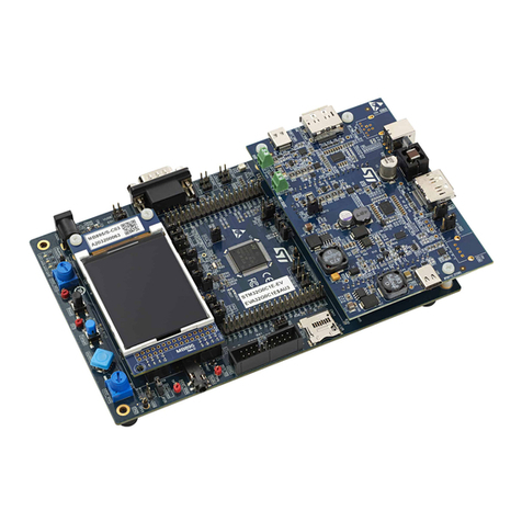
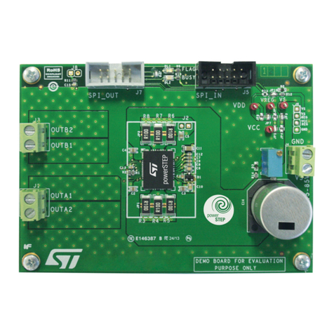
The AEK-POW-LDOV01J and AEK-POW-LDOV01S evaluation boards host, respectively, the L99VR01JTR and L99VR01STR
voltage regulator ICs, which are two different versions of the L99VR01.
Figure 1. AEK-POW-LDOV01J evaluation board
Figure 2. AEK-POW-LDOV01S evaluation board
The L99VR01 is a DC-DC voltage regulator designed for automotive applications (AEC-Q100 qualified). It can deliver up to 200
mA of load current and consumes around 1 μA when the regulator is disabled.
The operating input voltage is between 2.15 and 28 V, while a fixed selectable output voltage (0.8 V, 1.2 V, 1.5 V, 1.8 V, 2.5 V,
2.8 V, 3.3 V, or 5 V) is configurable.
Getting started with the AEK-POW-LDOV01J and AEK-POW-LDOV01S
automotive-grade LDOs with configurable output voltage
UM3028
User manual
UM3028 - Rev 1 - July 2022
For further information contact your local STMicroelectronics sales office. www.st.com

Figure 3. L99VR01JTR functional block
Figure 4. L99VR01STR functional block
The AEK-POW-LDOV01J and AEK-POW-LDOV01S boards can be used in a standalone configuration or with an external
microcontroller. In the latter case, the MCU provides a watchdog signal to the regulator to monitor the active connection.
These boards are included in the AutoDevKit ecosystem to enable a quick and easy prototyping for automotive and
transportation applications.
Warning: The AEK-POW-LDOV01J and AEK-POW-LDOV01S are evaluation tools for R&D laboratory use only.
They are not intended to be used inside a vehicle.
UM3028
UM3028 - Rev 1 page 2/37

1Getting started
1.1 Safety and protection mechanisms
The AEK-POW-LDOV01J evaluation board implements the following automotive safety mechanisms:
•Output voltage monitoring
It supervises the generated output voltage (VO). If the VO output voltage falls below the VOTH threshold
(equal to VO-10% VO), the RST pin is pulled low.
•Active connection monitoring (MCU connected configuration only)
For a continuous monitoring of the connection between the LDO and the MCU, a watchdog is used. The
watchdog signal (generated by the MCU and applied to the AEK-POW-LDOV01J WI pin) is a square wave
with a duty cycle equal to 50%. The frequency value depends on both the output voltage and the chosen C4
capacitor value (see the L99VR01JTR schematics). The LDO device monitors the watchdog signal provided
by the MCU. If the signal frequency is outside the range described above, the RST pin is pulled low. You can
disable the watchdog through a jumper on the AEK-POW-LDOV01J Vcw1 pin.
•Regulator enabling and disabling
The L99VR01JTR voltage regulator is enabled/disabled through the EN signal input.
•Overcurrent monitoring and lost ground protection
The overcurrent limit is set by regulating a current on the Ishort through an external potentiometer available
on the AEK-POW-LDOV01J. If the overcurrent limit is reached, the RST pin is pulled low.
•Thermal warning detection
To warn the microcontroller about a severe temperature increase of the LDO, a thermal warning output has
been implemented. If the device detects a junction temperature above 150°C, the thermal warning (TW)
output pin is pulled low, while the voltage regulator and all its features remain active.
•Overvoltage warning detection
The TW pin also provides diagnostics about the output overvoltage. To distinguish between a thermal and
an overvoltage warning event, two different signals are generated on the same TW output pin. A thermal
warning event detection sets the TW pin to low, whereas an output overvoltage event generates a square
wave (duty cycle 50% and period 300 microseconds) on the TW pin.
The AEK-POW-LDOV01S does not support safety features like watchdog, Ishort control, thermal and overvoltage
warning detections.
1.2 MCU connected configuration
In this configuration, the external MCU performs the following actions:
•generates signals (3.3 or 5 V) to control the output voltage selection thought the SELx pin;
• generates a signal to control the EN input pin (3 or 5 V);
• generates a square wave (3.3 or 5 V) to control the watchdog logic (for the AEK-POW-LDOV01J only)
• reads the TW pin to detect the thermal warning or overvoltage events (for the AEK-POW-LDOV01J only)
• reads the RST pin to detect if the VO output voltage is below a given threshold or to detect a wrong
watchdog frequency (for the AEK-POW-LDOV01J only)
• uses an ADC to monitor the voltage generated by the LDO
• generates a fixed voltage reference (VEXT - 3.3 or 5 V) to read the LDO signals properly.
Note: If the AEK-POW-LDV01x is connected to an external MCU, remove all the on-board jumpers.
1.3 Standalone configuration
In the standalone configuration:
•select the output voltage by using the Sel1, Sel2, or Sel3 jumpers;
• insert the EN1 jumper to enable the L99VR01 and remove it right after the power-up sequence;
• insert the Vcw1 jumper to disable the watchdog requirement (for the AEK-POW-LDOV01J only).
UM3028
Getting started
UM3028 - Rev 1 page 3/37
2Hardware architecture
The AEK-POW-LDOV01J and AEK-POW-LDOV01S evaluation boards are equipped with:
• CN1 connector: used only if the board is connected to an external microcontroller.
Table 1. CN1 pin description
Pin Description
Sel1 Sel2, Sel3 Output voltage selectors
EN Enable input
TW (for the AEK-POW-LDOV01J only) Thermal warning output and overvoltage warning output
WI (for the AEK-POW-LDOV01J only) Watchdog input
RST Reset output
VEXT Input external voltage reference (3.3 or 5 V)
GND Ground reference
VADC Output voltage. This pin can be used to read the output voltage via a configured
external ADC peripheral that belongs to the MCU.
• Jumpers: to be used in standalone working mode only.
Table 2. Jumper pin description
Pin Description
Sel1 Sel2, Sel3
Output voltage selectors.
To set SELx to high, put a jumper between the central position and ‘1’ position.
To set SELx to low, put a jumper between the central position and ‘0’ position.
EN1 Enable jumper.
To enable the board, mount the jumper and remove it right after.
Vcw1 (for the AEK-POW-LDOV01J only) Watchdog disable jumper.
In standalone mode, disable the watchdog by applying a jumper on Vcw1.
• Voltage connectors
Table 3. Voltage connector details
Connector Description
VS Operating DC power supply voltage range from 2.15 to 28 V
VOLDO output voltage
UM3028
Hardware architecture
UM3028 - Rev 1 page 4/37

2.1 Enable pin
The enable input (EN) enables/disables the L99VR01. A high-voltage signal switches the regulator on. When the
enable pin is set to low, the output is switched off. Then, the current consumption of the device is about 1 μA.
Figure 5. Enable and disable signals
The EN input pin or the EN1 jumper enable/disable the AEK-POW-LDOV01J/AEK-POW-LDOV01S, as follows:
• when the EN pin is set to high, it is forced to low and the output is switched off;
• when the EN pin is set to low, it is forced to high and the output is switched on;
• when the EN1 jumper is applied, the EN pin is forced to low and the output is switched off.
To change the output voltage while the regulator is on, apply a pulse signal to the EN input pin after the SELx pin
setting.
Figure 6. Pulse signal in case of output voltage changing
UM3028
Enable pin
UM3028 - Rev 1 page 5/37

2.2 Output voltage selection
The L99VR01 provides up to eight different output voltage options. The combination of its three digital input
selectors (SELx) determines the output voltage according to the following truth table.
Table 4. SELx pins: truth table
VO (volt) SEL1 SEL2 SEL3
5 1 1 1
3.3 1 1 0
2.8 1 0 1
2.5 1 0 0
1.8 0 1 1
1.5 0 1 0
1.2 0 0 1
0.8 (default) 0 0 0
The SELx pin configuration is acquired at the device startup (about 500 microseconds). Once the configuration is
set, the output voltage cannot be changed until the next EN pin transition. If all SELx pins are left unconnected,
the default configuration is selected.
2.3 Watchdog (for the AEK-POW-LDO01J only)
The watchdog is an automotive safety mechanism used to monitor a continuous connection with an external
MCU.
The watchdog signal (generated by the MCU and applied to the AEK-POW-LDOV01J WI pin) is a square wave
with a duty cycle equal to 50%. Its frequency value depends on both the output voltage and the chosen C4
capacitor value (see the L99VR01JTR schematics).
The table below lists the watchdog frequencies (Hz) related to the selectable output voltage.
Table 5. WI frequencies in Hz
VO (volt) WI frequency (Hz)
5 172
3.3 114
2.8 94
2.5 76
1.8 55
1.5 49
1.2 42
0.8 (default) 28
UM3028
Output voltage selection
UM3028 - Rev 1 page 6/37

2.4 Overvoltage warning (for the AEK-POW-LDO01J only)
The TW pin provides the output overvoltage (OV) diagnostic. To distinguish between a thermal warning and an
output overvoltage event, two different signals are generated on the same TW output pin. A thermal warning
event detection sets the TW pin low. An output overvoltage event generates a square wave on the TW pin. The
overvoltage detection has a higher priority than the thermal warning detection. Therefore, if both protections are
triggered, the generated signal is a square wave.
Figure 7. Overvoltage warning
UM3028
Overvoltage warning (for the AEK-POW-LDO01J only)
UM3028 - Rev 1 page 7/37

3Software architecture
According to the AutoDevKit paradigm, several MCU boards can be connected to the AEK-POW-LDOV01J/AEK-
POW-LDOV01S evaluation board. The smallest available MCU is the SPC582B Chorus 1M.
The AutoDevKit ecosystem fully supports the hardware. This ecosystem consists of:
• the SPC5-STUDIO development environment;
• the SPC5-UDESTK debug and firmware download tool;
• the STSW-AUTODEVKIT Eclipse plugin.
The AutoDevKit software includes a dedicated driver for the AEK-POW-LDOV01J/AEK-POW-LDOV01S as well
as demo codes.
3.1 SPC5-STUDIO
SPC5-STUDIO is an integrated development environment (IDE) based on Eclipse designed to assist the
development of embedded applications based on SPC5 Power Architecture 32-bit microcontrollers.
The package includes an application wizard to initiate projects with all the relevant components and key elements
required to generate the final application source code. It also contains straightforward software examples for each
MCU peripheral.
SPC5-STUDIO also features:
•the possibility of integrating other software products from the standard Eclipse marketplace
• free license GCC GNU C Compiler component
• support for industry-standard compilers
• support for multi-core microcontrollers
• PinMap editor to facilitate MCU pin configuration
Download the SPC5-UDESTK software to run and debug applications created with SPC5-STUDIO.
3.2 STSW-AUTODEVKIT
The STSW-AUTODEVKIT plug-in for Eclipse extends SPC5-STUDIO for automotive and transportation
applications.
STSW-AUTODEVKIT features:
• integrated hardware and software components, component compatibility checking, and MCU and peripheral
configuration tools
• the possibility of creating new system solutions from existing ones by adding or removing compatible
function boards
• new code can be generated immediately for any compatible MCU
• high-level application APIs to control each functional component, including the ones for the AEK-POW-
LDOV01J and AEK-POW-LDOV01S boards
The GUI helps configure interfaces, including SPI, and can automatically manage all relevant pin allocation and
deallocation operations.
3.3 AEK-POW-LDOV01x software library architecture
The drivers related to the AEK-POW-LDOV01x are included in a component belonging to the AutoDevKit software
(STSW-AUTODEVKIT) version 1.7.0 (or higher). The library is written in C and the target software is generated
automatically according to the code generation and pin allocation paradigm included in the AutoDevKit design
flow.
The AEK-POW-LDOV01x software library is based on a finite state machine (AEK-POWLDOV01x_fsm) called
by a timer (PIT peripheral on SPC58 microcontrollers). The minimum value selectable for the FSM frequency
is equal to 10 kHz, which ensures the correct detection of thermal and overvoltage warnings (for the AEK-POW-
LDOV01J only).
The AEK-POW-LDOV01x software library supports a multiple board allocation configured inside the dedicated
AutoDevKit GUI.
To simplify the management of multiple boards, a unique FSM is used in the driver and for each board allocated.
The current state is recorded.
UM3028
Software architecture
UM3028 - Rev 1 page 8/37

Figure 8. LDO driver finite state machine
The AEK-POW-LDOV01x states are:
•IDLE: initial state at power-up
•POWER ON: this state is reached when the AEK-POW-LDOV01x is enabled (through the pulse signal
applied to the EN pin)
•POWER OFF: this state is reached when the AEK-POW-LDOV01x is disabled (through the high signal
applied to the EN pin)
•RESET: this state detects a falling reset signal. It returns to the normal state when the VO output voltage
rises above VOTH and the watchdog frequency value is correct (for the AEK-POW-LDOV01J only)
•ERROR: the FSM enters this state when the absolute value of the difference between the VO voltage output
(read by the SARADC-12 bit) and the voltage output reference (selected by the SELx pin) is greater than a
voltage threshold equal to 5% of the voltage reference. In this state, the system is in a dangerous condition
and the LDO should be disabled
•NORMAL: this is the state of normal operating conditions. In this state, the AEK-POW-LDOV01x software
library is able to detect the thermal and overvoltage warning events (for the AEK-POW-LDOV01J
only).When the normal state is active, the AEK-POW-LDOV01x software library generates a WI (watchdog)
signal by using the E-MIOS peripheral with a fixed frequency whose value depends on the SELx
configuration pin (for the AEK-POW-LDOV01J only)
Note: The AEK-POW-LDOV01x software library supports both AEK-POW-LDOV01J and AEK-POW-LDOV01S
evaluation boards. If the user selects the AEK-POW-LDOV01S, the watchdog signal generation (WI), thermal,
and overvoltage detection events are disabled.
3.3.1 Init device
At power-up, the AEK-POW-LDOV01x initializes the E-MIOS peripheral in the microcontroller to generate the WI
signal (for the AEK-POW-LDOV01J only). The second step consists in initializing the ADC (SARADC-12bit) used
to read and monitor the VO output voltage provided by the voltage regulator.
The AEK-POW-LDOV01x software library includes a unique Init instruction with the following prototype:
void AEK_POW_LDOV01x_init(uint8_t AEK_POW_LDOV01x_n_device); where the
AEK_POW_LDOV01x_n_device represents the allocated AEK-POW-LDOV01x board.
Note: You can invoke void AEK_POW_LDOV01x_initAll() to initiate all the boards allocated.
3.3.2 Power on
The AEK-POW-LDOV01x activation requires an enable on transaction of the FSM (see Section 2.2 ).
The AEK-POW-LDOV01x software library includes the following power on instruction:
void AEK_POW_LDOV01x_power_on(uint8_t AEK_POW_LDOV01x_n_device);, where the
AEK_POW_LDOV01x_n_device represents the allocated AEK-POW-LDOV01x board.
UM3028
AEK-POW-LDOV01x software library architecture
UM3028 - Rev 1 page 9/37

Note: Before proceeding with the power on, set the output voltage by using the SELx pins.
3.3.3 Power off
To turn the AEK-POW-LDOV01x off, an enable off transaction is required.
The AEK-POW-LDOV01x software library includes the following power off instruction:
void AEK_POW_LDOV01x_power_off (uint8_t AEK_POW_LDOV01x_n_device);, where the
AEK_POW_LDOV01x_n_device represents the allocated AEK-POW-LDOV01x board.
3.3.4 Setting the output voltage
To set the AEK-POW-LDOV01x output voltage, configure the SELx pins.
The AEK-POW-LDOV01x software library includes an instruction for the output voltage setting:
void AEK_POW_LDOV01x_setOperationMode(AEK_POW_LDOV01x_op_mode_t op_mode, uint8_t
AEK_POW_LDOV01x_n_device);, where:
•AEK_POW_LDOV01x_n_device represents the allocated AEK-POW-LDOV01x board;
•AEK_POW_LDOV01x_op_mode_t is an enum typedef structure ( _0_8V, _1_2V, _1_5V, _1_8V, _2_5V,
_2_8_V, _3_3V, and _5_0V) used for the output voltage selection.
Note: Before proceeding with the power on, set the operating voltage by using the SELx pins.
3.3.5 Get device status
The AEK-POW-LDOV01x software library includes a get FSM status instruction:
AEK_POW_LDOV01x_sts_t AEK_POW_LDOV01x_getDeviceSts (uint8_t
AEK_POW_LDOV01x_n_device);, where:
•AEK_POW_LDOV01x_n_device represents the allocated AEK-POW-LDOV01x board;
•AEK_POW_LDOV01x_sts_t is an enum typedef structure (IDLE, POWER_OFF, POWER_ON, RESET,
ERROR, NORMAL).
3.3.6 Get warning status
The AEK-POW-LDOV01x software library includes a get warning status instruction to detect the warning
events while the FSM is in the normal status:
AEK_POW_LDOV01x_warning_sts_t AEK_POW_LDOV01x_getWarningStatus (uint8_t
AEK_POW_LDOV01x_n_device);, where:
•AEK_POW_LDOV01x_n_device represents the allocated AEK-POW-LDOV01x board;
•AEK_POW_LDOV01x_warning_sts_t is an enum typedef structure (THERMAL_WARNING,
OVERVOLTAGE_WARNING, NO_WARNING).
3.3.7 Get output voltage
The AEK-POW-LDOV01x software library includes an instruction to get the output voltage value read from the
SARADC:
float AEK_POW_LDOV01x_getVout (uint8_t AEK_POW_LDOV01x_n_device);, where:
•AEK_POW_LDOV01x_n_device represents the allocated AEK-POW-LDOV01x board;
UM3028
AEK-POW-LDOV01x software library architecture
UM3028 - Rev 1 page 10/37

4Demo in the AutoDevKit
4.1 How to create a sample application for the AEK-POW-LDOV01x
This example explains how to create an application for the AEK-POW-LDOV01J/AEK-POW-LDOV01S. The
microcontroller board used is the AEK-MCU-C1MLIT1.
Step 1. Create a new SPC5-STUDIO application for the SPC582B series microcontroller and add the following
components:
– SPC582Bxx Init Package Component RLA
– SPC582Bxx Low Level Drivers Component RLA
Important: Add these components immediately. Otherwise, the other components are not visible.
Step 2. Add the following additional components:
– AutoDevKit Init Package Component
– SPC582Bxx Platform Component RLA
– AEK-POW-LDOV01X Component RLA
Step 3. Select [AEK-POW-LDOV01x Component RLA] to open the [Application Configuration] window.
Figure 9. [AEK-POW-LDOV01x Component RLA] selection
UM3028
Demo in the AutoDevKit
UM3028 - Rev 1 page 11/37

Step 4. Click on [+] to add a new element to the board list.
Figure 10. Adding a new element
Step 5. Double-click on the newly added element to configure the board.
Step 6. Select the voltage regulator part number.
Figure 11. Voltage regulator selection
Step 7. Select the FSM frequency (the default value is 10 kHz).
Step 8. Select the ADC voltage reference (the default value is 5 V).
Step 9. Click the [Allocation] button below the AEK-POW-LDOV01x list and click [OK] in the confirmation
window.
This operation delegates the automatic pin allocation to the AutoDevKit.
Step 10. Generate and build the application using the appropriate icons in SPC5-STUDIO.
The project folder is then populated with new files, including the main.c and the component folder with
the AEK-POW-LDOV01x drivers.
Step 11. Open the main.c file and include the AEK_POW_LDOV01x.h file.
Step 12. Save, generate, and compile the application.
Step 13. Open the [Board View Editor] provided by the AutoDevKit.
This editor offers a graphical point-to-point guide on how to wire the boards.
Step 14. Connect the AEK-MCU-C1MLIT1 to a USB port on your PC using a mini-USB to USB cable.
Step 15. Launch SPC5-UDESTK-SW and open the debug.wsx file in the chosen application name UDE folder.
Step 16. Run and debug your code.
4.2 Available demos for the AEK-POW-LDOV01x
The AutoDevKit includes some voltage regulator demos available for the SPC58EC Chorus 4M
(SPC58ECxx_RLA AEK-POW-LDOV01x – DC – DC Voltage Regulator - Test Application) and SPC582B Chorus
1M (SPC582Bxx_RLA AEK-POW-LDOV01x – DC – DC Voltage Regulator - Test Application). The demos are
identical, but they are controlled by different MCUs.
UM3028
Available demos for the AEK-POW-LDOV01x
UM3028 - Rev 1 page 12/37

The AEK-POW-LDOV01J board demo goal is to generate a fixed output voltage (5 V). If an overvoltage warning
or thermal warning event occurs, the regulator is switched off.
Figure 12. Demo code
Note: If the AEK-POW-LDOV01J is connected to the load, set the correct VO output voltage by using the
AEK_POW_LDOV01x_setOperationMode API.
4.2.1 How to upload the demos
Follow the procedure below to import the demos into SPC5-STUDIO.
Step 1. Select [Import samples from application library] from the [Common tasks] panel.
An [Import application Wizard] appears.
UM3028
Available demos for the AEK-POW-LDOV01x
UM3028 - Rev 1 page 13/37

Step 2. Insert the appropriate MCU family details.
Figure 13. MCU family selection
Step 3. Select the desired application from the library.
Figure 14. Application selection
Step 4. Click the [Finish] button.
UM3028
Available demos for the AEK-POW-LDOV01x
UM3028 - Rev 1 page 14/37

5APIs
void AEK_POW_LDOV01x_init(uint8_t AEK_POW_LDOV01x_n_device);
This function initializes the AEL_POW_LDOV01x.
void AEK_POW_LDOV01x_initAll();
This function initializes all the AEL_POW_LDOV01x.
void AEK_POW_LDOV01x_power_on(uint8_t AEK_POW_LDOV01x_n_device);
This function turns on the AEK_POW_LDOV01x.
void AEK_POW_LDOV01x_power_off(uint8_t AEK_POW_LDOV01x_n_device);
This function turns off the AEK_POW_LDOV01x.
void AEK_POW_LDOV01x_setOperationMode(AEK_POW_LDOV01x_op_mode_t op_mode, uint8_t
AEK_POW_LDOV01x_n_device);
This function sets the output voltage (0.8 V, 1.2 V, 1.5 V, 1.8 V, 2.5 V, 2.8 V, 3.3 V, or 5 V) for the
AEK_POW_LDOV01x.
AEK_POW_LDOV01x_sts_t AEK_POW_LDOV01x_getDeviceSts(uint8_t AEK_POW_LDOV01x_n_device);
This function gets the AEK_POW_LDOV01x status (IDLE, POWER_OFF, POWER_ON, RESET, ERROR,
NORMAL)
AEK_POW_LDOV01x_warning_sts_t AEK_POW_LDOV01x_getWarningStatus(uint8_t AEK_POW_LDOV01x_n_device);
This function gets the AEK_POW_LDV01x warning status (THERMAL_WARNING, OVERVOLTAGE_WARNING,
NO_WARNING).
float AEK_POW_LDOV01x_getVout(uint8_t AEK_POW_LDOV01x_n_device);
This function gets the output voltage read from SARADC when the AEK_POW_LDOV01x is connected to an
external MCU.
UM3028
APIs
UM3028 - Rev 1 page 15/37

6Test results
Figure 15. Enable pulse signal waveform generated by an external MCU connected to the AEK-POW-
LDOV01J
UM3028
Test results
UM3028 - Rev 1 page 16/37

Figure 16. Watchdog signal waveform generated by an external MCU connected to the AEK-POW-
LDOV01J (operating voltage selected = 5 V)
UM3028
Test results
UM3028 - Rev 1 page 17/37

Figure 17. Output voltage waveform generated by the AEK-POW-LDOV01J after power on (operating
voltage selected = 5 V)
UM3028
Test results
UM3028 - Rev 1 page 18/37

Figure 18. Thermal warning waveform generated by the AEK-POW-LDOV01J after power on (operating
voltage selected = 5 V)
UM3028
Test results
UM3028 - Rev 1 page 19/37

Figure 19. Overvoltage warning waveform generated by the AEK-POW-LDOV01J (operating voltage
selected = 5 V)
UM3028
Test results
UM3028 - Rev 1 page 20/37
This manual suits for next models
1
Table of contents
Other ST Motherboard manuals

ST
ST SPC58XXADPT64S User manual

ST
ST STEVAL-USBPD45H Administrator Guide

ST
ST STEVAL-PCC001V1 User manual

ST
ST Nucleo STM32F302R8 User manual

ST
ST STEVAL-SMARTAG2 User manual

ST
ST STM32100B-EVAL User manual

ST
ST STM32H735G-DK User manual

ST
ST eMotion STEVAL-MKI109V1 User manual

ST
ST STM32G4 Nucleo-32 User manual

ST
ST STEVAL-IFS002V2 User manual

ST
ST AEKD-AICAR1 User manual

ST
ST STEVAL-OET001V1 User manual

ST
ST EVALSPEAr320PLC User manual

ST
ST AEKD-USBTYPEC1 User manual

ST
ST STM3220G-EVAL User manual

ST
ST X-NUCLEO-IDB04A1 User manual

ST
ST B-L4S5I-IOT01A User manual

ST
ST X-NUCLEO-CCA02M1 User manual

ST
ST STEVAL-IHM022V1 User manual

ST
ST SPC58NG-DISP User manual