ST NUCLEO-F207ZG User manual

December 2017 DocID028599 Rev 7 1/82
1
UM1974
User manual
STM32 Nucleo-144 boards
Introduction
The STM32 Nucleo-144 boards (NUCLEO-F207ZG, NUCLEO-F303ZE, NUCLEO-F412ZG,
NUCLEO-F413ZH, NUCLEO-F429ZI, NUCLEO-F439ZI, NUCLEO-F446ZE,
NUCLEO-F722ZE, NUCLEO-F746ZG, NUCLEO-F756ZG, NUCLEO-F767ZI and
NUCLEO-H743ZI) provide an affordable and flexible way for users to try out new concepts
and build prototypes, by choosing from the various combinations of performance and power
consumption features provided by the STM32 microcontroller. The ST Zio connector, which
extends the Arduino™Uno V3 connectivity, and the ST morpho headers provide an easy
means of expanding the functionality of the Nucleo open development platform with a wide
choice of specialized shields. The STM32 Nucleo-144 boards do not require any separate
probe as they integrate the ST-LINK/V2-1 debugger/programmer. The STM32 Nucleo-144
boards come with the comprehensive free software libraries and examples available with
the STM32Cube MCU Package, as well as a direct access to the Arm®Mbed Enabled™on-
line resources at http://mbed.org.
Figure 1. Nucleo-144 board (top view) Figure 2. Nucleo-144 board (bottom view)
www.st.com
All manuals and user guides at all-guides.com
all-guides.com

Contents UM1974
2/82 DocID028599 Rev 7
Contents
1 Features . . . . . . . . . . . . . . . . . . . . . . . . . . . . . . . . . . . . . . . . . . . . . . . . . . . 6
2 Product marking . . . . . . . . . . . . . . . . . . . . . . . . . . . . . . . . . . . . . . . . . . . . 7
3 Ordering information . . . . . . . . . . . . . . . . . . . . . . . . . . . . . . . . . . . . . . . . 7
4 Conventions . . . . . . . . . . . . . . . . . . . . . . . . . . . . . . . . . . . . . . . . . . . . . . . 9
5 Quick start . . . . . . . . . . . . . . . . . . . . . . . . . . . . . . . . . . . . . . . . . . . . . . . . . 9
5.1 Getting started . . . . . . . . . . . . . . . . . . . . . . . . . . . . . . . . . . . . . . . . . . . . . . 9
5.2 System requirements . . . . . . . . . . . . . . . . . . . . . . . . . . . . . . . . . . . . . . . . 10
5.3 Development toolchains . . . . . . . . . . . . . . . . . . . . . . . . . . . . . . . . . . . . . . 10
6 Hardware layout and configuration . . . . . . . . . . . . . . . . . . . . . . . . . . . . 11
6.1 Mechanical drawing . . . . . . . . . . . . . . . . . . . . . . . . . . . . . . . . . . . . . . . . . 14
6.2 Cuttable PCB . . . . . . . . . . . . . . . . . . . . . . . . . . . . . . . . . . . . . . . . . . . . . . 15
6.3 Embedded ST-LINK/V2-1 . . . . . . . . . . . . . . . . . . . . . . . . . . . . . . . . . . . . . 16
6.3.1 Drivers . . . . . . . . . . . . . . . . . . . . . . . . . . . . . . . . . . . . . . . . . . . . . . . . . . 16
6.3.2 ST-LINK/V2-1 firmware upgrade . . . . . . . . . . . . . . . . . . . . . . . . . . . . . . 17
6.3.3 Using the ST-LINK/V2-1 to program and debug the on-board STM32 . 17
6.3.4 Using ST-LINK/V2-1 to program and debug an external STM32
application . . . . . . . . . . . . . . . . . . . . . . . . . . . . . . . . . . . . . . . . . . . . . . . 18
6.4 Power supply and power selection . . . . . . . . . . . . . . . . . . . . . . . . . . . . . . 20
6.4.1 Power supply input from ST-LINK/V2-1 USB connector . . . . . . . . . . . . 21
6.4.2 External power supply inputs . . . . . . . . . . . . . . . . . . . . . . . . . . . . . . . . . 22
6.4.3 External power supply output . . . . . . . . . . . . . . . . . . . . . . . . . . . . . . . . 24
6.5 LEDs . . . . . . . . . . . . . . . . . . . . . . . . . . . . . . . . . . . . . . . . . . . . . . . . . . . . 24
6.6 Push-buttons . . . . . . . . . . . . . . . . . . . . . . . . . . . . . . . . . . . . . . . . . . . . . . 25
6.7 JP5 (IDD) . . . . . . . . . . . . . . . . . . . . . . . . . . . . . . . . . . . . . . . . . . . . . . . . . 25
6.8 OSC clock . . . . . . . . . . . . . . . . . . . . . . . . . . . . . . . . . . . . . . . . . . . . . . . . 25
6.8.1 OSC clock supply . . . . . . . . . . . . . . . . . . . . . . . . . . . . . . . . . . . . . . . . . 25
6.8.2 OSC 32 KHz clock supply . . . . . . . . . . . . . . . . . . . . . . . . . . . . . . . . . . . 26
6.9 USART communication . . . . . . . . . . . . . . . . . . . . . . . . . . . . . . . . . . . . . . 26
6.10 USB OTG FS or device . . . . . . . . . . . . . . . . . . . . . . . . . . . . . . . . . . . . . . 27
All manuals and user guides at all-guides.com

DocID028599 Rev 7 3/82
UM1974 Contents
3
6.11 Ethernet . . . . . . . . . . . . . . . . . . . . . . . . . . . . . . . . . . . . . . . . . . . . . . . . . . 28
6.12 Solder bridges . . . . . . . . . . . . . . . . . . . . . . . . . . . . . . . . . . . . . . . . . . . . . 29
6.13 Extension connectors . . . . . . . . . . . . . . . . . . . . . . . . . . . . . . . . . . . . . . . . 33
6.14 ST Zio connectors . . . . . . . . . . . . . . . . . . . . . . . . . . . . . . . . . . . . . . . . . . 37
6.15 ST morpho connector . . . . . . . . . . . . . . . . . . . . . . . . . . . . . . . . . . . . . . . . 69
Appendix A Electrical schematics . . . . . . . . . . . . . . . . . . . . . . . . . . . . . . . . . . . . 73
Appendix B Federal Communications Commission (FCC)
and Industry Compliance Statements . . . . . . . . . . . . . . . . . . . . . . . 80
B.1 FCC Compliance Statement . . . . . . . . . . . . . . . . . . . . . . . . . . . . . . . . . . . 80
B.1.1 Part 15.19 . . . . . . . . . . . . . . . . . . . . . . . . . . . . . . . . . . . . . . . . . . . . . . . . 80
B.1.2 Part 15.105 . . . . . . . . . . . . . . . . . . . . . . . . . . . . . . . . . . . . . . . . . . . . . . . 80
B.1.3 Part 15.21 . . . . . . . . . . . . . . . . . . . . . . . . . . . . . . . . . . . . . . . . . . . . . . . . 80
B.2 IC Compliance Statement . . . . . . . . . . . . . . . . . . . . . . . . . . . . . . . . . . . . . 80
B.2.1 Compliance Statement . . . . . . . . . . . . . . . . . . . . . . . . . . . . . . . . . . . . . . 80
B.2.2 Déclaration de conformité. . . . . . . . . . . . . . . . . . . . . . . . . . . . . . . . . . . . 80
Revision history . . . . . . . . . . . . . . . . . . . . . . . . . . . . . . . . . . . . . . . . . . . . . . . . . . . . 81
All manuals and user guides at all-guides.com

List of tables UM1974
4/82 DocID028599 Rev 7
List of tables
Table 1. Ordering information . . . . . . . . . . . . . . . . . . . . . . . . . . . . . . . . . . . . . . . . . . . . . . . . . . . . . . . 7
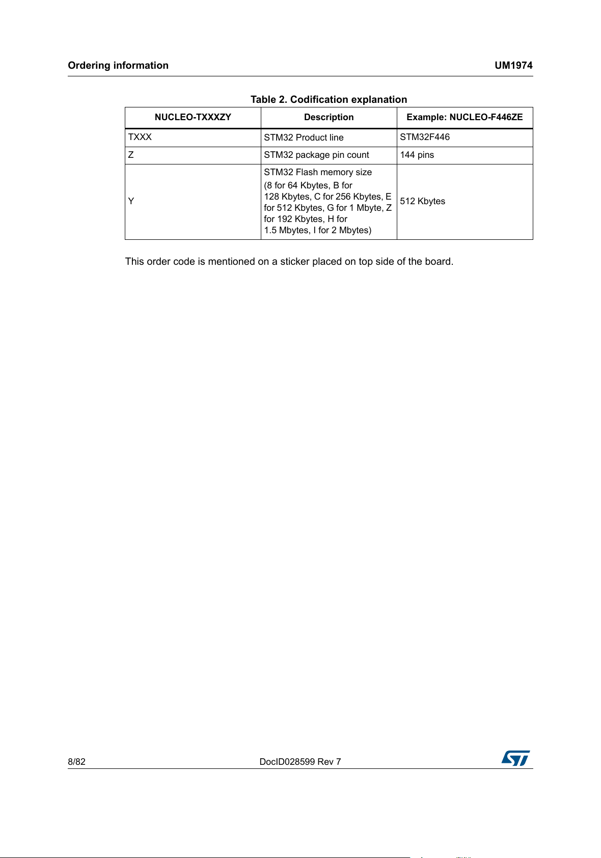
Table 2. Codification explanation . . . . . . . . . . . . . . . . . . . . . . . . . . . . . . . . . . . . . . . . . . . . . . . . . . . . 8
Table 3. ON/OFF conventions . . . . . . . . . . . . . . . . . . . . . . . . . . . . . . . . . . . . . . . . . . . . . . . . . . . . . . 9
Table 4. CN4 states of the jumpers . . . . . . . . . . . . . . . . . . . . . . . . . . . . . . . . . . . . . . . . . . . . . . . . . 16
Table 5. Debug connector CN6 (SWD) . . . . . . . . . . . . . . . . . . . . . . . . . . . . . . . . . . . . . . . . . . . . . . 19
Table 6. JP1 configuration table . . . . . . . . . . . . . . . . . . . . . . . . . . . . . . . . . . . . . . . . . . . . . . . . . . . . 21
Table 7. External power sources . . . . . . . . . . . . . . . . . . . . . . . . . . . . . . . . . . . . . . . . . . . . . . . . . . . 22
Table 8. Power related jumper . . . . . . . . . . . . . . . . . . . . . . . . . . . . . . . . . . . . . . . . . . . . . . . . . . . . . 23
Table 9. USART3 pins . . . . . . . . . . . . . . . . . . . . . . . . . . . . . . . . . . . . . . . . . . . . . . . . . . . . . . . . . . . 26
Table 10. USB pins configuration . . . . . . . . . . . . . . . . . . . . . . . . . . . . . . . . . . . . . . . . . . . . . . . . . . . . 27
Table 11. Ethernet pins. . . . . . . . . . . . . . . . . . . . . . . . . . . . . . . . . . . . . . . . . . . . . . . . . . . . . . . . . . . . 28
Table 12. Solder bridges. . . . . . . . . . . . . . . . . . . . . . . . . . . . . . . . . . . . . . . . . . . . . . . . . . . . . . . . . . . 29
Table 13. NUCLEO-F746ZG, NUCLEO-F756ZG and NUCLEO-F767ZI
pin assignments. . . . . . . . . . . . . . . . . . . . . . . . . . . . . . . . . . . . . . . . . . . . . . . . . . . . . . . . . 38
Table 14. NUCLEO-F446ZE and NUCLEO-F722ZE pin assignments . . . . . . . . . . . . . . . . . . . . . . . . 43
Table 15. NUCLEO-F303ZE pin assignments . . . . . . . . . . . . . . . . . . . . . . . . . . . . . . . . . . . . . . . . . . 47
Table 16. NUCLEO-F207ZG pin assignments . . . . . . . . . . . . . . . . . . . . . . . . . . . . . . . . . . . . . . . . . . 51
Table 17. NUCLEO-F429ZI and NUCLEO-F439ZI pin assignments . . . . . . . . . . . . . . . . . . . . . . . . . 55
Table 18. NUCLEO-F412ZG pin assignments . . . . . . . . . . . . . . . . . . . . . . . . . . . . . . . . . . . . . . . . . . 59
Table 19. NUCLEO-F413ZH pin assignments . . . . . . . . . . . . . . . . . . . . . . . . . . . . . . . . . . . . . . . . . . 62
Table 20. NUCLEO-H743ZI pin assignments. . . . . . . . . . . . . . . . . . . . . . . . . . . . . . . . . . . . . . . . . . . 66
Table 21. ST morpho connector for NUCLEO-F207ZG, NUCLEO-F412ZG,
NUCLEO-F413ZH, NUCLEO-F429ZI, NUCLEO-F439ZI, NUCLEO-F446ZE,
NUCLEO-F722ZE, NUCLEO-F746ZG, NUCLEO-F756ZG,
NUCLEO-F767ZI and NUCLEO-H743ZI . . . . . . . . . . . . . . . . . . . . . . . . . . . . . . . . . . . . . . 70
Table 22. ST morpho connector for NUCLEO-F303ZE . . . . . . . . . . . . . . . . . . . . . . . . . . . . . . . . . . . 71
Table 23. Document revision history . . . . . . . . . . . . . . . . . . . . . . . . . . . . . . . . . . . . . . . . . . . . . . . . . 81
All manuals and user guides at all-guides.com

DocID028599 Rev 7 5/82
UM1974 List of figures
5
List of figures
Figure 1. Nucleo-144 board (top view). . . . . . . . . . . . . . . . . . . . . . . . . . . . . . . . . . . . . . . . . . . . . . . . . 1
Figure 2. Nucleo-144 board (bottom view). . . . . . . . . . . . . . . . . . . . . . . . . . . . . . . . . . . . . . . . . . . . . . 1
Figure 3. Hardware block diagram. . . . . . . . . . . . . . . . . . . . . . . . . . . . . . . . . . . . . . . . . . . . . . . . . . . 11
Figure 4. Top layout . . . . . . . . . . . . . . . . . . . . . . . . . . . . . . . . . . . . . . . . . . . . . . . . . . . . . . . . . . . . . . 12
Figure 5. Bottom layout . . . . . . . . . . . . . . . . . . . . . . . . . . . . . . . . . . . . . . . . . . . . . . . . . . . . . . . . . . . 13
Figure 6. Nucleo-144 board mechanical drawing in millimeter . . . . . . . . . . . . . . . . . . . . . . . . . . . . . 14
Figure 7. Nucleo-144 board mechanical drawing in mil . . . . . . . . . . . . . . . . . . . . . . . . . . . . . . . . . . . 15
Figure 8. USB composite device . . . . . . . . . . . . . . . . . . . . . . . . . . . . . . . . . . . . . . . . . . . . . . . . . . . . 17
Figure 9. Connecting the STM32 Nucleo-144 board to program the on-board STM32 . . . . . . . . . . . 18
Figure 10. Using ST-LINK/V2-1 to program the STM32 on an external application . . . . . . . . . . . . . . 20
Figure 11. NUCLEO-F207ZG, NUCLEO-F429ZI, NUCLEO-F439ZI, NUCLEO-F746ZG,
NUCLEO-F756ZG, NUCLEO-F767ZI and NUCLEO-H743ZI . . . . . . . . . . . . . . . . . . . . . . 33
Figure 12. NUCLEO-F303ZE. . . . . . . . . . . . . . . . . . . . . . . . . . . . . . . . . . . . . . . . . . . . . . . . . . . . . . . . 34
Figure 13. NUCLEO-F412ZG and NUCLEO-F413ZH . . . . . . . . . . . . . . . . . . . . . . . . . . . . . . . . . . . . . 35
Figure 14. NUCLEO-F446ZE and NUCLEO-F722ZE . . . . . . . . . . . . . . . . . . . . . . . . . . . . . . . . . . . . . 36
Figure 15. Top and power . . . . . . . . . . . . . . . . . . . . . . . . . . . . . . . . . . . . . . . . . . . . . . . . . . . . . . . . . . 74
Figure 16. MCU . . . . . . . . . . . . . . . . . . . . . . . . . . . . . . . . . . . . . . . . . . . . . . . . . . . . . . . . . . . . . . . . . . 75
Figure 17. ST-LINK/V2-1 . . . . . . . . . . . . . . . . . . . . . . . . . . . . . . . . . . . . . . . . . . . . . . . . . . . . . . . . . . . 76
Figure 18. USB . . . . . . . . . . . . . . . . . . . . . . . . . . . . . . . . . . . . . . . . . . . . . . . . . . . . . . . . . . . . . . . . . . 77
Figure 19. Ethernet PHY with RJ45 connector . . . . . . . . . . . . . . . . . . . . . . . . . . . . . . . . . . . . . . . . . . 78
Figure 20. Extension connectors . . . . . . . . . . . . . . . . . . . . . . . . . . . . . . . . . . . . . . . . . . . . . . . . . . . . . 79
All manuals and user guides at all-guides.com

Features UM1974
6/82 DocID028599 Rev 7
1 Features
The STM32 Nucleo-144 boards offer the following features:
•STM32 microcontroller in LQFP144 package
•Ethernet compliant with IEEE-802.3-2002 (depending on STM32 support)
•USB OTG or full-speed device (depending on STM32 support)
•3 user LEDs
•2 push-buttons: USER and RESET
•LSE crystal:
– 32.768 kHz crystal oscillator
•Board connectors:
– USB with Micro-AB
– Ethernet RJ45
•Expansion connectors:
– ST Zio including Arduino™Uno V3
–STmorpho
•Flexible power-supply options: ST-LINK USB VBUS or external sources
•On-board ST-LINK/V2-1 debugger/programmer with SWD connector:
– ST-LINK/V2-1 standalone kit capability
– USB re-enumeration capability: virtual COM port, mass storage, debug port
•Comprehensive free software libraries and examples available with the STM32Cube
package
•Supported by wide choice of Integrated Development Environments (IDEs) including
IAR™, Keil®, GCC-based IDEs, Arm®Mbed™
•ARM®Mbed Enabled™(see http://mbed.org)
All manuals and user guides at all-guides.com
all-guides.com

DocID028599 Rev 7 7/82
UM1974 Product marking
81
2 Product marking
Evaluation tools marked as “ES” or “E” are not yet qualified and therefore not ready to be
used as reference design or in production. Any consequences deriving from such usage will
not be at ST charge. In no event, ST will be liable for any customer usage of these
engineering sample tools as reference design or in production.
“E” or “ES” marking examples of location:
•On the targeted STM32 that is soldered on the board (for illustration of STM32 marking,
refer to the STM32 datasheet “Package information” paragraph at the www.st.com
website).
•Next to the evaluation tool ordering part number that is stuck or silk-screen printed on
the board.
This board features a specific STM32 device version which allows the operation of any
stack or library. This STM32 device shows a "U" marking option at the end of the standard
part number and is not available for sales.
3 Ordering information
To order the Nucleo-144 board corresponding to the targeted STM32, use the order code
given below in Table 1:
The meaning of the NUCLEO-TXXXZY codification is explained in Table 2 with an example:
Table 1. Ordering information
Order code Target STM32
NUCLEO-F207ZG STM32F207ZGT6
NUCLEO-F303ZE STM32F303ZET6
NUCLEO-F412ZG STM32F412ZGT6
NUCLEO-F413ZH STM32F413ZHT6
NUCLEO-F429ZI STM32F429ZIT6
NUCLEO-F439ZI STM32F439ZIT6
NUCLEO-F446ZE STM32F446ZET6
NUCLEO-F722ZE STM32F722ZET6
NUCLEO-F746ZG STM32F746ZGT6
NUCLEO-F756ZG STM32F756ZGT6
NUCLEO-F767ZI STM32F767ZIT6
NUCLEO-H743ZI STM32H743ZIT6
All manuals and user guides at all-guides.com

Ordering information UM1974
8/82 DocID028599 Rev 7
This order code is mentioned on a sticker placed on top side of the board.
Table 2. Codification explanation
NUCLEO-TXXXZY Description Example: NUCLEO-F446ZE
TXXX STM32 Product line STM32F446
Z STM32 package pin count 144 pins
Y
STM32 Flash memory size
(8 for 64 Kbytes, B for
128 Kbytes, C for 256 Kbytes, E
for 512 Kbytes, G for 1 Mbyte, Z
for 192 Kbytes, H for
1.5 Mbytes, I for 2 Mbytes)
512 Kbytes
All manuals and user guides at all-guides.com

DocID028599 Rev 7 9/82
UM1974 Conventions
81
4 Conventions
Table 3 provides the conventions used for the ON and OFF settings in the present
document.
In this document the references for all information that is common to all sale types, are
“STM32 Nucleo-144 board” and “STM32 Nucleo-144 boards”.
5 Quick start
The STM32 Nucleo-144 board is a low-cost and easy-to-use development kit, used to
evaluate and start a development quickly with an STM32 microcontroller in LQFP144
package.
Before installing and using the product, accept the Evaluation Product License Agreement
from the www.st.com/epla webpage. For more information on the STM32 Nucleo-144 and
for demonstration software, visit the www.st.com/stm32nucleo webpage.
5.1 Getting started
Follow the sequence below to configure the Nucleo-144 board and launch the
demonstration application (for components location refer to Figure 4: Top layout):
1. Check jumper position on the board:
JP1 OFF (PWR-EXT) selected (see Section 6.4.1: Power supply input from ST-
LINK/V2-1 USB connector for more details)
JP3 on U5V (Power source) selected (for more details see Table 7: External power
sources)
JP5 ON (IDD) selected (for more details see Section 6.7: JP5 (IDD))
CN4 ON selected (for more details see Table 4: CN4 states of the jumpers)
2. For the correct identification of the device interfaces from the host PC and before
connecting the board, install the Nucleo USB driver available on the
www.st.com/stm32nucleo website.
3. To power the board connect the STM32 Nucleo-144 board to a PC with a USB cable
‘Type-A to Micro-B’ through the USB connector CN1 on the ST-LINK. As a result, the
green LED LD6 (PWR) and LD4 (COM) light up and the red LED LD3 blinks.
Table 3. ON/OFF conventions
Convention Definition
Jumper JPx ON Jumper fitted
Jumper JPx OFF Jumper not fitted
Solder bridge SBx ON SBx connections closed by solder or 0 ohm resistor
Solder bridge SBx OFF SBx connections left open
All manuals and user guides at all-guides.com

Quick start UM1974
10/82 DocID028599 Rev 7
4. Press button B1 (left button).
5. Observe the blinking frequency of the three LEDs LD1 to LD3 changes, by clicking on
the button B1.
6. The software demonstration and the several software examples, that allow the user to
use the Nucleo features, are available at the www.st.com/stm32nucleo webpage.
7. Develop an application, using the available examples.
5.2 System requirements
•Windows®OS (7, 8 and 10), Linux®or MacOS™
•USB Type-A to Micro-B cable
5.3 Development toolchains
•Arm®Keil®: MDK-ARM™(a)
•IAR™: EWARM(a)
•GCC-based IDEs: free SW4STM32 from AC6
•Arm®Mbed Enabled™
a. On Windows only.
All manuals and user guides at all-guides.com

DocID028599 Rev 7 11/82
UM1974 Hardware layout and configuration
81
6 Hardware layout and configuration
The STM32 Nucleo-144 board is designed around the STM32 microcontrollers in a 144-pin
LQFP package.
Figure 3 shows the connections between the STM32 and its peripherals (ST-LINK/V2-1,
push-buttons, LEDs, USB, Ethernet, ST Zio connectors and ST morpho headers).
Figure 4 and Figure 5 show the location of these features on the STM32 Nucleo-144 board.
The mechanical dimensions of the board are showed in Figure 6 and Figure 7.
Figure 3. Hardware block diagram
06Y9
(PEHGGHG
67/,1.9
670
0LFURFRQWUROOHU
5(6(7
6:'
67PRUSKRH[WHQVLRQKHDGHU
,2
50,,86%
%
567
%
86(5
,2
=LR&RQQHFWRU
/('
/'
67/,1.3DUW
0&83DUW
/('
/'
0LFUR$%
86%
FRQQHFWRU
=LR&RQQHFWRU
5-
FRQQHFWRU
0LFUR%
86%
FRQQHFWRU
All manuals and user guides at all-guides.com
all-guides.com

Hardware layout and configuration UM1974
12/82 DocID028599 Rev 7
Figure 4. Top layout
06Y9
&1
67/,1.1XFOHR
VHOHFWRU
8
670
0LFURFRQWUROOHU
&1
6:'FRQQHFWRU
&1
67/,1.0LFUR%
86%FRQQHFWRU
/'
UHGJUHHQ/('
&20
%
8VHUEXWWRQ
-3
,''PHDVXUHPHQW
/'/'
8VHU/('V
&1
67=LRFRQQHFWRU
&1
67PRUSKR
SLQKHDGHU
%
5HVHWEXWWRQ
/'
3RZHUJUHHQ/('
6%
9UHJXODWRURXWSXW
&1
67PRUSKRSLQKHDGHU
&1
&1
=,2FRQQHFWRU
&1
=,2FRQQHFWRU
&1
8VHU86%
FRQQHFWRU
/'
5HG/('67/,1.9
3RZHURYHUFXUUHQWDODUP
&1
(WKHUQHW
5-
FRQQHFWRU
-3
3:5(;7
-3
3RZHUVRXUFHVHOHFWLRQ
/'86%RYHU
FXUUHQW
/'86%
9%86
67=LRFRQQHFWRU
All manuals and user guides at all-guides.com

DocID028599 Rev 7 13/82
UM1974 Hardware layout and configuration
81
Figure 5. Bottom layout
06Y9
6%6%6%6%
5(6(59('
6%6% 6%6%
'()$8/7
6%6:2
6%0&2
All manuals and user guides at all-guides.com

Hardware layout and configuration UM1974
14/82 DocID028599 Rev 7
6.1 Mechanical drawing
Figure 6. Nucleo-144 board mechanical drawing in millimeter
06Y9
All manuals and user guides at all-guides.com

DocID028599 Rev 7 15/82
UM1974 Hardware layout and configuration
81
Figure 7. Nucleo-144 board mechanical drawing in mil
6.2 Cuttable PCB
The STM32 Nucleo-144 board is divided into two parts: ST-LINK and target STM32. The
ST-LINK part of the PCB can be cut out to reduce the board size. In this case the remaining
target STM32 part can only be powered by VIN, E5V and 3.3 V on ST morpho connector
CN11, or VIN and 3.3 V on ST Zio connector CN8. It is still possible to use the ST-LINK part
to program the STM32, using wires between CN6 and SWD available signals on the ST
morpho connector (SWCLK CN11 pin 15, SWDIO CN11 pin 13 and NRST CN11 pin 14).
06Y9
All manuals and user guides at all-guides.com

Hardware layout and configuration UM1974
16/82 DocID028599 Rev 7
6.3 Embedded ST-LINK/V2-1
The ST-LINK/V2-1 programming and debugging tool is integrated in the STM32 Nucleo-144
board.
The ST-LINK/V2-1 makes the STM32 Nucleo-144 board mbed enabled.
The embedded ST-LINK/V2-1 supports only SWD for STM32 devices. For information about
debugging and programming features refer to ST-LINK/V2 in-circuit debugger/programmer
for STM8 and STM32, User manual (UM1075), which describes in details all the ST-
LINK/V2 features.
The changes versus ST-LINK/V2 version are listed below.
New features supported on ST-LINK/V2-1:
•USB software re-enumeration
•Virtual com port interface on USB
•Mass storage interface on USB
•USB power management request for more than 100mA power on USB
Features not supported on ST-LINK/V2-1:
•SWIM interface
•Minimum supported application voltage limited to 3 V
There are two different ways to use the embedded ST-LINK/V2-1, depending on the jumper
state (see Table 4):
•Program/debug the STM32 on board
•Program/debug the STM32 in an external application board, using a cable connected
to SWD connector CN6
6.3.1 Drivers
Before connecting the Nucleo-144 board to a Windows 7, Windows 8 or Windows XP PC
via USB, a driver for ST-LINK/V2-1 must be installed. It can be downloaded from the
www.st.com website.
In case the STM32 Nucleo-144 board is connected to the PC before installing the driver, the
PC device manager may report some Nucleo interfaces as “Unknown”.
To recover from this situation, after installing the dedicated driver, the association of
“Unknown” USB devices found on the STM32 Nucleo-144 board to this dedicated driver,
must be updated in the device manager manually.
Note: It is recommended to proceed using USB Composite Device, as shown in Figure 8.
Table 4. CN4 states of the jumpers
Jumper state Description
Both CN4 jumpers ON ST-LINK/V2-1 functions enabled for on-board programming
(default). See Section 6.3.3.
Both CN4 jumpers OFF ST-LINK/V2-1 functions enabled for external CN6 connector
(SWD supported). See Section 6.3.4.
All manuals and user guides at all-guides.com
all-guides.com

DocID028599 Rev 7 17/82
UM1974 Hardware layout and configuration
81
Figure 8. USB composite device
6.3.2 ST-LINK/V2-1 firmware upgrade
The ST-LINK/V2-1 embeds a firmware upgrade mechanism for in-situ upgrade through the
USB port. As the firmware may evolve during the lifetime of the ST-LINK/V2-1 product (for
example new functionalities, bug fixes, support for new microcontroller families), it is
recommended to keep the ST-LINK/V2-1 firmware up to date before starting to use the
STM32 Nucleo-144 board. The latest version of this firmware is available from the
www.st.com website.
6.3.3 Using the ST-LINK/V2-1 to program and debug the on-board STM32
To program the on-board STM32, place the two jumpers marked in red on the connector
CN4, as shown in Figure 9. The CN6 connector must not be used, since it could disturb the
communication with the STM32 microcontroller of the Nucleo-144 board.
All manuals and user guides at all-guides.com

Hardware layout and configuration UM1974
18/82 DocID028599 Rev 7
Figure 9. Connecting the STM32 Nucleo-144 board to program the on-board STM32
6.3.4 Using ST-LINK/V2-1 to program and debug an external STM32
application
It is very easy to use the ST-LINK/V2-1 to program the STM32 on an external application.
Simply remove the two jumpers from CN4, as shown in Figure 10 and connect the
application to the CN6 debug connector according to Table 5.
Note: SB111 NRST (target STM32 RESET) must be OFF when CN6 pin 5 is used in an external
application.
06Y9
&1MXPSHUV21
&1
6:'FRQQHFWRU
All manuals and user guides at all-guides.com

DocID028599 Rev 7 19/82
UM1974 Hardware layout and configuration
81
Table 5. Debug connector CN6 (SWD)
Pin CN6 Designation
1 VDD_TARGET VDD from application
2 SWCLK SWD clock
3 GND ground
4 SWDIO SWD data input/output
5 NRST RESET of target STM32
6 SWO Reserved
All manuals and user guides at all-guides.com

Hardware layout and configuration UM1974
20/82 DocID028599 Rev 7
Figure 10. Using ST-LINK/V2-1 to program the STM32 on an external application
6.4 Power supply and power selection
The power supply is provided either by the host PC through the USB cable or by an external
source: VIN (7 V-12 V), E5V (5 V) or +3.3 V power supply pins on CN8 or CN11. In case VIN,
E5V or +3.3 V is used to power the Nucleo-144 board, this power source must comply with
the standard EN-60950-1: 2006+A11/2009 and must be Safety Extra Low Voltage (SELV)
with limited power capability.
06Y9
&1MXPSHUV2))
&1
6:'FRQQHFWRU
All manuals and user guides at all-guides.com
Other manuals for NUCLEO-F207ZG
1
This manual suits for next models
11
Table of contents
Other ST Motherboard manuals

ST
ST SPC560B-DIS User manual

ST
ST STEVAL-QUADV01 User manual

ST
ST M24LR64-R User manual

ST
ST STM32H757I-EVAL User manual

ST
ST STM32L1 Series Installation and operating instructions

ST
ST STEVAL-BLUEPLUG1 User manual

ST
ST STM32G081B-EVAL User manual

ST
ST AEKD-USBTYPEC1 User manual

ST
ST STM32L476G-EVAL User manual

ST
ST BlueNRG-LP User manual

ST
ST STM32G0C1E-EV User manual

ST
ST STM32091C-EVAL User manual

ST
ST STM32 Nucleo User manual

ST
ST STM32756G-EVAL User manual

ST
ST EVAL-FDA903U-SA User manual

ST
ST EnFilm EFL1K0AF39 User manual

ST
ST STM32CubeF4 User manual

ST
ST STM8L15LPBOARD User manual

ST
ST X-NUCLEO-IDW01M1 User manual

ST
ST STMPE801 User manual