ST STEVAL-ISB041V1 User manual

Chipsmall Limited consists of a professional team with an average of over 10 year of expertise in the distribution
of electronic components. Based in Hongkong, we have already established firm and mutual-benefit business
relationships with customers from,Europe,America and south Asia,supplying obsolete and hard-to-find components
to meet their specific needs.
With the principle of “Quality Parts,Customers Priority,Honest Operation,and Considerate Service”,our business
mainly focus on the distribution of electronic components. Line cards we deal with include
Microchip,ALPS,ROHM,Xilinx,Pulse,ON,Everlight and Freescale. Main products comprise
IC,Modules,Potentiometer,IC Socket,Relay,Connector.Our parts cover such applications as commercial,industrial,
and automotives areas.
We are looking forward to setting up business relationship with you and hope to provide you with the best service
and solution. Let us make a better world for our industry!
Contact us
Tel: +86-755-8981 8866 Fax: +86-755-8427 6832
Email & Skype: [email protected]om Web: www.chipsmall.com
Address: A1208, Overseas Decoration Building, #122 Zhenhua RD., Futian, Shenzhen, China

March 2017
DocID030421 Rev 1
1/21
www.st.com
UM2185
User manual
Getting started with the STEVAL-ISB041V1 Li-Ion/Li-Po battery
power management evaluation board based on STBC02
Introduction
The STEVAL-ISB041V1 evaluation board is based on STBC02 Li-Ion and Li-Po linear battery
management device, integrating a CC-CV charger algorithm, an always-on LDO, smart-reset Watchdog,
a protection circuit module (PCM) and a dual SPDT switch matrix.
The device is able to charge batteries at a 450 mA continuous maximum current with few external
passive components, so the whole application can be reduced down to as little as 4.5 mm x 5 mm.
The module can deliver 60 mA charging current and supply the system up to 300 mA while powered by
a standard 5 V output DC power supply. It is suitable for battery operated equipment, wearable devices,
fitness portable devices, MP3 players, healthcare and medical instrumentation, body worn equipment,
etc.
Figure 1: STEVAL-ISB041V1 evaluation board

Contents
UM2185
2/21
DocID030421 Rev 1
Contents
1Getting started................................................................................. 5
1.1 Board overview .................................................................................5
1.2 Input/output connectors.....................................................................5
1.3 Test procedure and technical recommendations...............................7
1.3.1 Recommended equipment ................................................................. 7
1.3.2 Procedure to test a typical full charging cycle .................................... 8
2GND pins........................................................................................ 10
3Schematic diagram........................................................................ 14
4PCB layout ..................................................................................... 15
5STBC02: block diagram and ballout ............................................ 16
6Revision history ............................................................................ 19
Appendix A General handling precautions.................................. 20

UM2185
List of tables
DocID030421 Rev 1
3/21
List of tables
Table 1: Input/output connector: pin description.........................................................................................5
Table 2: STEVAL-ISB041V1 evaluation board pin functions ...................................................................10
Table 3: Ball description............................................................................................................................17
Table 4: Document revision history ..........................................................................................................19

List of figures
UM2185
4/21
DocID030421 Rev 1
List of figures
Figure 1: STEVAL-ISB041V1 evaluation board..........................................................................................1
Figure 2: STEVAL-ISB041V1 evaluation board pinout...............................................................................7
Figure 3: STBC02 battery proper connection and routing ........................................................................11
Figure 4: Hall current probe ......................................................................................................................12
Figure 5: STEVAL-ISB041V1 circuit schematic........................................................................................14
Figure 6: STEVAL-ISB041V1 PCB layout: top side..................................................................................15
Figure 7: STEVAL-ISB041V1 PCB layout: bottom side............................................................................15
Figure 8: STBC02 block diagram..............................................................................................................16
Figure 9: STBC02 (flipchip30, 2.25 mm x 2.59 mm package): ballout, top view......................................16

UM2185
Getting started
DocID030421 Rev 1
5/21
1 Getting started
1.1 Board overview
The STEVAL-ISB041V1 evaluation board size is 50 mm x 50 mm.
The PCB is made by using FR4 glass epoxy support with 4 copper layers.
The device features:
Charges single-cell Li-Ion/Li-Po batteries with CC-CV algorithm and charge
termination
Fast charge current programmable from 1 mA to 450 mA
Pre-charge current programmable from 1 mA to 450 mA
Adjustable floating voltage up to 4.45 V
Integrated always-on low quiescent LDO regulator
Battery over-charge and over-discharge protections
Overcurrent protection
Shipping mode exit input
Integrated dual 3 Ω SPDT load switches
Integrated smart reset / watchdog logic
Single wire control interface
RoHS compliant
1.2 Input/output connectors
The input/output connectors (J1-J23) provide the necessary probing signals:
Kelvin connection points for input and output voltage;
enable signal input;
multiple GND connection;
s-wire input
Table 1: Input/output connector: pin description
Connector
Pin
number
Symbol
Signal name
Pin description
J1
2
D
CEN
Charger enable pin
3
C
RESET_NOW
Smart reset input signal
4
S-w
SW_SEL
Serial s-wire input
5
CEN
CEN
Charger enable pin
6
CHG
CHG
Charging/fault flag
7
Wup
Wake-Up
Shipping mode exit input
pin
J3
2
MS2
Reserved
3
MS3
Reserved
4
nRES
Smart reset output signal
5
rPEND
Smart reset output signal
J7
2
ISET
ISET
Fast-charge current
programming resistor

Getting started
UM2185
6/21
DocID030421 Rev 1
Connector
Pin
number
Symbol
Signal name
Pin description
3
IPRE
IPRE
Pre-charge current
programming resistor
J8
2
LDO
LDO
LDO output
3
LDO_S
LDO
LDO output sensing
J9
2
IN
IN
Input supply voltage
3
IN_S
IN
Input supply voltage
sensing
J10
2
BAT_S
BAT
Battery sensing
3
BAT
BAT
Battery - positive terminal
4
----
----
Reserved
5
NTC
NTC
Battery temperature
monitor pin
J11
2
SYS
SYS
System output
3
SYS_S
SYS
System output sensing
J13
2
BATMS
BATMS
Battery voltage
measurement pin
J15
2
1_I
SW1_I
3
1_OA
SW1_OA
4
1_OB
SW1_OB
5
2_I
SW2_I
6
2_OA
SW2_OA
7
2_OB
SW2_OB
J19
VBUS
----
IN
Input supply voltage
J23
2
BATSNS
BAT
Battery voltage sensing
3
BATSNSFV
BATSNSFV
Floating voltage sensing
J1, J3, J7, J8, J9, J10,
J11, J13, J15, J23
1
GND
Ground connection

UM2185
Getting started
DocID030421 Rev 1
7/21
Figure 2: STEVAL-ISB041V1 evaluation board pinout
1.3 Test procedure and technical recommendations
STBC02 linear battery management IC is designed to manage the whole battery charging
procedure, powering the system through the power path node output (SYS unregulated
voltage rail) via a low quiescent linear regulator output.
Being a linear device, the charger is most efficient when the input voltage is only slightly
above the battery voltage (VIN = 4.55 to 5.4 V).
A low input voltage (inferior to the sum of the OUT voltage plus the dropout voltage) results
in degraded performance. Excessive input voltage (>5.4 V) results in power dissipation and
reduced performance (it halves the charge current if thermal warning is reached) due to the
IC thermal management protection circuit.
The IC is set to 16 V and is not damaged with a lower VIN voltage, but it is disabled by any
VIN voltage over the overvoltage protection threshold (5.9 V).
Section 1.3.2: "Procedure to test a typical full charging cycle" describes the procedure to
test and observe a typical full charging cycle. The CC-CV algorithm is linked to the battery
voltage level. If a battery having VBAT>3 V is plugged, the pre-charge phase is skipped and
the device directly enters in fast charge mode.
1.3.1 Recommended equipment
Bench power supply (+5 VDC) with current limit set to ~1-2 A or USB wall adaptor with
micro USB plug;
oscilloscope with one current and three high impedance voltage probes;
programmable digital waveform generator (or standard MCU to implement digital
sequence).

Getting started
UM2185
8/21
DocID030421 Rev 1
1.3.2 Procedure to test a typical full charging cycle
The three most important STBC02 functional modes are:
battery mode: VBAT valid range, system up and running, VIN invalid range;
shutdown mode: device supplied by battery but in shutdown mode;
VIN mode: VIN valid range present.
The charger is designed to be used with Li-Ion batteries (Li-Ion nominal battery voltage is
3.7-3.8V). VBAT range is 0 (dead battery) to 4.5 V (overcharged battery). The device input
operating supply voltage is 4.5 to 5.5 VDC.
The procedure to demonstrate this power path charger is:
1
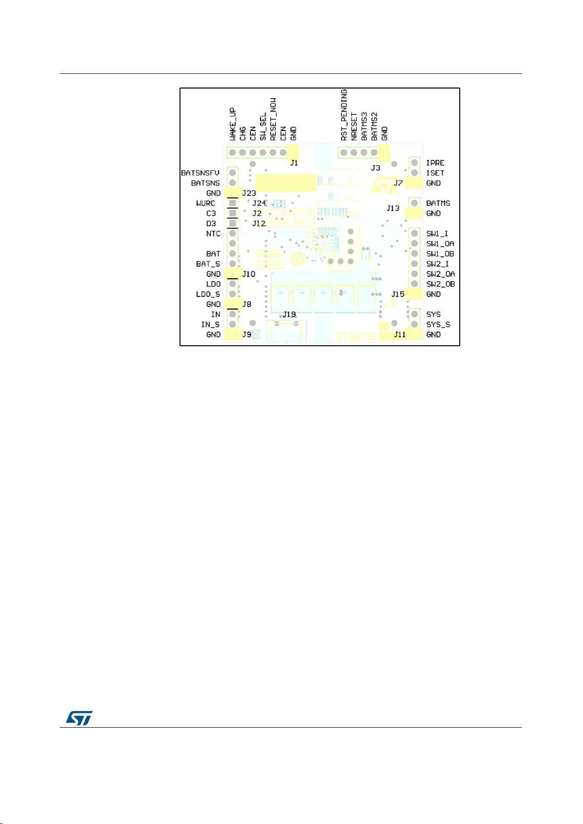
Connect one high impedance probe to J1/pin6 (CHG) vs GND.
2
Connect one high impedance probe to J10/pin2 (BAT_S) vs. GND.
3
Place the current probe on the positive battery terminal wire.
4
Connect (fully discharged) battery (e.g. 2.5 V) to J10/pin3 (VBAT) vs. GND.
5
Connect power supply ~5.0 V to J9/pin3 (IN) vs GND.
6
Battery starts charging by IPRE charging current. Verify that IBAT is ~6 mA (10%
of IFAST).
7
Connect a 33 Ω, ½-W resistor to J8/pin3 (LDO) vs. GND.
8
With a high impedance probe, verify that LDO (node LDO_S - J8/pin2) output is 3.1
V.
CHG toggles (6 Hz).
When battery voltage level exceeds VPRE (3 V), the charging current changes
from IPRE to IFAST and increases to ~ 60 mA (IFAST setup). During this phase,
CHG is still toggling at the same frequency if no warning/alarm is detected. In this
condition, LDO and system are powered by the power supply.
9
Verify with high impedance probe that SYS voltage (J11/pin2) is approximately 5 V
(IN node level minus internal MOS drop).
You can stop the charging cycle by a jumper to short CEN to GND (short J1/pin2 to
J1/pin1) just to verify CEN pin is functional.
10
Verify that the charger stops.
CHG changes state and its level goes low.
11
Remove short CEN to GND to continue charging.
12
Charge the battery fully
At a certain battery level (typical 4.2 V), charging current starts falling and battery
voltage level remains constant at VFLOAT level.
13
Battery charging is automatically stopped when battery charging current drops
under 5 % of IFAST.
14
Disconnect charger to observe device behavior in battery mode.
Battery starts discharging to supply the load connected to LDO output; the current
probe measures a negative value (~VLDO/resistive load).
15
Verify through high impedance probe that SYS_S voltage (J11/pin2) is VBAT voltage
minus VBAT equal to VSYS MOSFET RDSON multiplied by load current.
16
Remove resistive load from the LDO output.

UM2185
Getting started
DocID030421 Rev 1
9/21
17
Disconnect and reconnect battery.
SYS and LOD node are not supplied now, as the device is in shutdown mode. To
enter battery mode, you have to pull WakeUp pin to VBAT level (to be precise, the
WakeUp pin has to exceed 3.0 V level).

GND pins
UM2185
10/21
DocID030421 Rev 1
2 GND pins
All GND pins are connected by a dedicated metallic layer: the evaluation board GND
routing strategy does not feature separated GND branches. The only exception is the
battery negative terminal connection.
Table 2: STEVAL-ISB041V1 evaluation board pin functions
Name
Function
IN_S
Sensing: to measure input voltage directly on C1 capacitor
IN
Forcing: input dedicated to charger positive terminal
LDO_S
Sensing: to measure input voltage directly on C3 capacitor
LDO
Forcing: output pin dedicated to linear voltage regulator loading
BAT_S
Sensing: to measure battery voltage directly on C4 capacitor
BAT
Forcing: pin dedicated to battery positive terminal
NTC
NTC pin can be used to measure NTC pin voltage, to force NTC pin voltage by
external voltage, or to connect dedicated NTC resistor when R4 is disassembled
BATSNS
This pin is dedicated to measure the BATSNS ball voltage. If R15 is removed, this
pin can be used to sense the battery voltage closer to the battery positive terminal
BATSNSFV
This pin is dedicated to measure BATSNSFV ball voltage. R3 can be used to
increase VFLOAT
WAKE_UP
WakeUp –Shipping Mode exit: input dedicated to wakeup device by connecting
Wakeup to BAT
Pin internally pulled-down.
CHG
Charger indication pin: indicates valid input voltage by state (high or low) or
charging status and fault conditions by toggling at different frequency.
CEN
Charger enable pin 0 = disabled floating = 1 = enabled. The pin is pulled up
internally.
CEN<0.4 V is taken as 0, CEN>1.6 V is taken as 1
Range 0.4 to 1.6 V as well as exceeding LDO nominal value is no allowed.
SW_SEL
Swire digital input
RESET_NOW
Digital input to reset logic
NRESET
Digital reset output signal
RST_PENDING
Digital input t reset logic
IPRE
Pre-charge current programming resistor node: pin dedicated to measure IPRE
resistor voltage.
ISET
Fast-charge current programming resistor node: pin dedicated to measure ISET
resistor voltage
BATMS
Battery voltage measurement pin. When enabled by swire, BAT voltage is
connected to this pin through an internal switch with equivalent RON-BATMS.
SW1_I
Load switch SPDT1 input
SW1_OA
Load switch SPDT1 output A
SW1_OB
Load switch SPDT1 output B
SW2_I
Load switch SPDT2 input

UM2185
GND pins
DocID030421 Rev 1
11/21
Name
Function
SW2_OA
Load switch SPDT2 output A
SW2_OB
Load switch SPDT2 output B
SYS
Forcing: output pin dedicated to SYS loading
SYS_S
Sensing: to measure system voltage directly on C2 capacitor
NTC
NTC is assembled on board (fixed value 10 kΩ, resistor R4). If real NTC use is requested,
remove R4 and connect the real element between NTC node and GND. Couple this NTC
element to the battery body properly.
BAT node
BAT node is reserved for battery positive terminal only. It is highly recommended to not
connect any other circuits (e.g., workarounds, bias for any circuit) to this node.
The figure below shows the correct BATSNS and BATSNSFV resistor routing to battery
positive connector terminal for measurement accuracy.
Figure 3: STBC02 battery proper connection and routing
To avoid fault state conditions or other problems during device evaluation phase, it is
recommended to use Hall effect oscilloscope current probes.

GND pins
UM2185
12/21
DocID030421 Rev 1
Figure 4: Hall current probe
Avoid connecting serial resistors between battery pack and device to measure
current voltage drop.
Battery protection
STBC02 works well when the charger is plugged; battery protection is activated in case of
fully discharged battery.
Safety timers do not support abnormally long delay between BAT node rise
(protection stimulation) and protection deactivation.
SW_SEL
input only
internal pull-down: 500 k
recommended operation voltage range: 0 V to LDO voltage level
Idle in LOW (pull down recommended when not in use)
single-wire peripheral communication pin
via bitstream, the device can be controlled: charging current can be halved, switches
can be switched on or off, and device can be (when in battery mode) suspended (shut
down mode to avoid battery consumption).
CEN
input
internal pull-up: 500 k to LDO
low = disabled charger
high = enabled charger
charger restart function
CHG
output
open drain
external pull-up: ~10 k

UM2185
GND pins
DocID030421 Rev 1
13/21
WakeUp
input
internal pull-down: 500 k to GND
tactile switch to battery (low to high transition) wakes up the device
RESET circuit
STBC02 is equipped with a multipurpose reset circuit. The mode can be selected by s-wire
bus:
smart reset generator in Smart reset mode (default after POR)
watchdog in Watchdog mode
Smart reset mode application example
Battery operated waterproof solutions or minimalistic devices (wearable sport wrap,
single ear headset) may not have any buttons. When the software crashes, the only
way to reset the device (processor) is by USB plug.
After each USB connection, RST_PENDING triggers the processor to save all data
4000 miliseconds before the nRESET pulse triggers reset. The signal RESET_NOW
can reset the processor earlier when all data has been saved and the processor is
ready.
Watchdog mode application example
The processor code contains a routine to periodically maintain the RESET_CLEAR signal.
When software crashes, the RESET_CLEAR pin is not toggled, the STBC02 timer
overflows and the generated nRESET pulse resets the processor. RST_PENDING follows
nRESET signal (RST_SIGNAL is not used in Watchdog mode).
nRESET pin
output signal
open drain output
50 µs in battery mode / 25 µs in VIN mode pulse duration.
Active low
No internal resistor integrated: external pull-down requested.
RST_PENDING pin
output signal
totem pole output: no external resistor requested
RESET_NOW pin (called also RESET_CLEAR in watchdog mode)
input signal
external pull-down highly recommended
referred to LDO level
smart reset mode: low to high transition forces immediate nRESET
watchdog mode: high level at RESET_NOW pin clears Watchdog timer
(RESET_NOW high to low transition enables counter, timer starts counting from zero,
nRESET is generated after watchdog period if RESET_NOW is kept low).

Schematic diagram
UM2185
14/21
DocID030421 Rev 1
3 Schematic diagram
Figure 5: STEVAL-ISB041V1 circuit schematic
1.0uF
C3
P1
GND
10uF
C1
1.0µF
C2
3.3kR1
33kR2
GND
GND
0R R3
10k R4
!DNP
R6
!DNP
R5
10kR9
10k/!DNP
R11
100kR12
470 R7
4.7uF
C4
ISET
IPRE
IN
IN_S
GND
GND
SW2_OB
SW1_I
SW1_OB
SW2_I
SW1_OA
SW2_OA
GND
GND
LDO
SYS_S
SYS
LDO
LDO_S
CHG
CEN
RESET_NOW
RST_PENDING
nRESET
SW_SEL
BATMS
NTC
BATSNSFV
BATMS2
BATMS3
GND
BAT
BATSNS
BAT
GND
BAT_S
BAT
WAK E_UP
100kR14
GND
100kR10
GND
GND
P9
IN
F5
SYS
C5
SW1_I
F3
SW1_OA
E4
SW1_OB
E3
SW2_I
E2
SW2_OA
F2
SW2_OB
F1
ISET
A4
IPRE
D4
GND
A3
AGND
B4
WAK E_UP D2
BATA5
BATSNSFV A2
BATSNS B3
NTCD1
BATMSC4
SW_SEL C1
nRESET C2
RST_PENDING B2
RESET_NOW A1
CENB1
CHGE1
LDO F4
IN
E5
SYS
D5
BATB5
D3
D3
C3
C3
U1
STBC0x_FC30_2269x2610
SW_SEL
STBC02
RST_PENDING
nRESET
RESET_NOW
C1
B2
C2
A1
!DNP/10k
R8
!DNP/10k
R13
LDO
GND
GND
GND
RST_PENDING
nRESET
BATM S3
BATM S2
1
2
3
4
5
6
7
J1
SW_SEL
CEN
WAKE_UP
CHG
GND
1
2
3
4
5
J3
RESET_NOW
CEN
C
D
GND
ID
DP
DM
VBUS
SHIELD
J19
!DNP
C10
!DNP
R16
GNDGND
IN
GND
BAT
NTC
SYS
IN
BATSNS
BATSNSFV
LDO
LDO_S
GND
GND
GND
GND
1
2
3
J8
IN_S
1
2
3
J9
SYS_S
1
2
3
J11
GND
BAT_S
1
2
3
4
5
J10
1
2
3
J23
J20
GND
J22 GND
J16
LDO
J17
IN
J18 BAT
J21 SYS
BATMS
ISET
IPRE
SW1_I
SW1_OA
SW1_OB
SW2_I
SW2_OA
SW2_OB
GND
1
2
3
J7
1
2
3
4
5
6
7
J15GND
1
2
J13GND
!DNP
R18
! DNP C12
GND
! DNP C11
GND
WAK E_UP
J24
WURCQ1

UM2185
PCB layout
DocID030421 Rev 1
15/21
4 PCB layout
Figure 6: STEVAL-ISB041V1 PCB layout: top side
Figure 7: STEVAL-ISB041V1 PCB layout: bottom side

STBC02: block diagram and ballout
UM2185
16/21
DocID030421 Rev 1
5 STBC02: block diagram and ballout
Figure 8: STBC02 block diagram
Figure 9: STBC02 (flipchip30, 2.25 mm x 2.59 mm package): ballout, top view

UM2185
STBC02: block diagram and ballout
DocID030421 Rev 1
17/21
Table 3: Ball description
Bump name
Alternative
bump name
Description
Power
IN
E5-F5
Input supply voltage. Bypass this pin to ground with a
2.2 µF capacitor
BAT
A5-B5
Battery positive terminal. Bypass this pin to GND with
a 4.7 µF ceramic capacitor
SYS
C5-D5
System output. Bypass this pin to ground with a 2.2
µF ceramic capacitor
LDO
F4
3.1 V LDO output. Bypass this pin to ground with a 1
µF ceramic capacitor
NTC
D1
Battery temperature monitor pin
AGND
B4
Analog Ground
Connect together with the
same ground layer
GND
A3
GROUND
Prog
ISET
A4
Fast-charge current programming resistor
IPRE
D4
Pre-charge current programming resistor
Sensing
BATMS
C4
Battery voltage measurement pin
BATSNS
B3
Battery voltage sensing. Connect as close as possible
to the battery positive terminal
BATSNSFV
A2
Floating voltage sensing. Connect as close as
possible to the battery positive terminal
Digital
I/Os
CEN
B1
Charger enable pin. Active high. 500 kΩ internal pull-
up (to LDO)
CHG
E1
Charging/fault Flag. Active low (open drain output)
WAKE-UP
D2
Shipping mode exit input pin. Active high. 500 kΩ
internal pull-down
SW_SEL
C1
Load switch selection input
nRESET
C2
Smart reset output signal (open drain output)
RST_PENDING
B2
Reset output signal (Totem pole output)
RESET_NOW
A1
Smart reset input signal (referred to LDO level);
RESET_CLEAR when watchdog is enabled
Switch
Matrix
SW1_I
F3
Load switch SPDT1
input (connect to 1.8 to
5 V range)
Decoupling capacitors are
recommended on input
and output pins for noise
minimization.
These switches are not
voltage regulated.
SW1_OA
E4
Load switch SPDT1
output A
(enabled/disabled
PMOS)
SW1_OB
E3
Load switch SPDT1
output B
(enabled/disabled
PMOS)
SW2_I
E2
Load switch SPDT2
input (connect to 1.8 to
5 V range)

STBC02: block diagram and ballout
UM2185
18/21
DocID030421 Rev 1
Bump name
Alternative
bump name
Description
SW2_OA
F2
Load switch SPDT2
output A
(enabled/disabled
PMOS)
SW2_OB
F1
Load switch SPDT2
output B
(enabled/disabled
PMOS)
NC
C3-D3
Not connected

UM2185
Revision history
DocID030421 Rev 1
19/21
6 Revision history
Table 4: Document revision history
Date
Version
Changes
28-Mar-2017
1
Initial release.
Table of contents
Other ST Motherboard manuals

ST
ST VIPower VIPer22A-E Installation and operating instructions

ST
ST STEVAL-IPC002V1 User manual

ST
ST eMotion STEVAL-MKI109V1 User manual

ST
ST Teseo-VIC3DA User manual

ST
ST UM2248 User manual

ST
ST EVAL-L99H02XP User manual

ST
ST STM3221G-EVAL User manual

ST
ST PractiSPIN UM0696 User manual

ST
ST Nucleo STM32F302R8 User manual

ST
ST AEK-SNS-2TOFM1 User manual