ST UM2414 User manual

Introduction
The STEVAL-IOM001V1 industrial IO-Link physical master evaluation board is based on the L6360 transceiver and is designed
to comply with applicable industrial EMC standards.
It provides an affordable and easy-to-use development platform for single-port to quad-port IO-Link master applications. By
default, the STEVAL-IOM001V1 is configured as IO-Link Port 1.
The evaluation board can be connected to an STM32 Nucleo development board like the NUCLEO-F446RE or NUCLEO-
F401RE via its ST morpho connectors.
You can obtain the board individually or as part of the P-NUCLEO-IOM01M1 development system, which includes a STEVAL-
IOM001V1 evaluation board and a NUCLEO-F446RE development board flashed with IO-Link stack (v1.1).
Figure 1. STEVAL-IOM001V1 IO-Link physical master evaluation board
Getting started with the IO-Link PHY master evaluation board with STM32 Nucleo
compatibility
UM2414
User manual
UM2414 - Rev 2 - April 2021
For further information contact your local STMicroelectronics sales office.
www.st.com

1Hardware and software requirements
The STEVAL-IOM001V1 is designed to be connected to one of the following STM32 Nucleo boards:
•NUCLEO-F446RE
•NUCLEO-F401RE
Figure 2. STEVAL-IOM001V1 plus STM32 Nucleo board
To complete the system, you need the following items:
•a Windows® (version 7 or above) PC
• a USB type A to mini-B USB cable to connect the STM32 Nucleo to the PC
• the STSW-IOM001 firmware and software package installed on the user PC
• a 24 V power supply
UM2414
Hardware and software requirements
UM2414 - Rev 2 page 2/22

2STEVAL-IOM001V1 evaluation board overview
The IO-Link PHY master evaluation board is equipped with the L6360 transceiver featuring the IO-Link physical
master and an IPS161H single high-side switch with extended diagnostic features (for safety integrity level SIL2-
and SIL3-compliant systems) to supply an external high capacitance IO-Link load on the L+ rail.
2.1 Features
• IO-Link master PHY based on L6360
•Interrupt diagnostics pin
• I²C and UART interface
• SPI (slave) interface
• 65 mA selectable (3.3 or 5.0 V) linear regulator
• CQ (push-pull) and L+ (high side) switches
• IQ additional IEC61131-2 type 1 digital input
• L+ and CQ overload and overheating protections with non-dissipative cut-off function
• QFN-26L (3.5x5x1 mm) package
• Operating voltage range from 18 to 32.5 V
• Additional high side switch for L+ heavy loads (IPS161H)
• LEDs for status and diagnostics
• Ground and VCC wire break protections
• EMC compliance with IEC61000-4-2, IEC61000-4-3, IEC61000-4-5
• Equipped with ST morpho connectors
• CE certified
• RoHS and China RoHS compliant
2.2 Digital section
The digital section is associated with the STM32 interface and the signals to control the L6360 IO-Link transceiver
and IPS161H high side switch.
UM2414
STEVAL-IOM001V1 evaluation board overview
UM2414 - Rev 2 page 3/22

Figure 3. STEVAL-IOM001V1 expansion board digital interface components
UM2414
Digital section
UM2414 - Rev 2 page 4/22

2.2.1 ST morpho connectors
The STEVAL-IOM001V1 communicates with the STM32 Nucleo board microcontroller and accesses the STM32
peripheral and GPIO resources through ST morpho connectors CN7 and CN10. These connectors also transfer
digital supply voltages between the STM32 Nucleo development board and the STEVAL-IOM001V1 expansion
board.
The following tables map the correspondence between the ST morpho connectors and microcontroller signals.
Table 1. Digital signals on CN7
Connector pin Signal STM32F4 port Drop jumper Notes
8, 19, 20, 22 GND - - -
24 VIN - - -
21
OUTCQ
PB7
R129
Not mounted
OL-OFF R170
28
ENCQ
PA0
R103 Not mounted
INCQ R115 Not mounted
30
ENL+
PA1
R104 Not mounted
OUTCQ R119 Not mounted
32 IRQ PA4 R7 Mounted
34 IRQ PB0 R117 Not mounted
35 ENL+ PC2 R124 Not mounted
36 RST PC1 R108 Not mounted
37 IRQ PC3 R137 Not mounted
38 ENCQ PC0 R3 Mounted
Table 2. Digital signals on CN10
Connector pin Signal STM32F4 port Drop jumper Notes
1 OUTIQ PC9 R116 Not mounted
2 ENCQ PC8 R133 Not mounted
3 SCL PB8 R1 Mounted
4 INCQ PC6 R134 Not mounted
5 SDA PB9 R2 Mounted
6 OUTCQ PC5 R139 Not mounted
9, 20, 32 GND - - -
11 ENCQ PA5 R143 Not mounted
13 ENL+ PA6 R4 Mounted
15 L+_ON PA7 R163 Not mounted
17 OUTIQ PB6 R106 Not mounted
19 OUTCQ PC7 R109 Not mounted
21 INCQ PA9 R5 Mounted
22 L+ ON PB2 R164 Not mounted
23
SCL
PA8
R111
Not mounted
ENL+ R114
UM2414
Digital section
UM2414 - Rev 2 page 5/22

Connector pin Signal STM32F4 port Drop jumper Notes
24 IRQ PB1 R107 Not mounted
25
SCL
PB10
R161
Not mounted
INCQ R105
26 L+ ON PB15 R165 Not mounted
27
L+_ON
PB4
R162 Mounted
SDA R122 Not mounted
28 OUTIQ PB14 R126 Not mounted
29 RST PB5 R8 Mounted
30 OUTIQ PB13 R136 Not mounted
31 SDA PB3 R132 Not mounted
33 OUTCQ PA10 R9 Mounted
34 ENL+ PC4 R135 Not mounted
The table below describes the functionality of each signal:
Table 3. Description of digital signals
Signal Functionality
ENL+ GPIO (out) controlling the ENL+ pin of L6360 (U1)
ENCQ GPIO (out) controlling the ENCQ pin of L6360 (U1)
INCQ UART (TX) controlling INCQ pin of L6360 (U1)
OUTCQ UART (RX) controlling OUTCQ pin of L6360 (U1)
SCL Serial clock line controlling I2C SCL pin of L6360 (U1)
SDA Serial data line controlling I2C SDA pin of L6360 (U1)
RST GPIO (out) controlling the RST pin of L6360 (U1)
IRQ GPIO (externa event) controlling the IRQ pin of L6360 (U1)
OUTIQ(1) Not used by default, it can be configured on a UART (RX) to control the OUTIQ pin of L6360 (U1)
L+_ON GPIO (out) controlling the IN pin of IPS161H (U2)
OL-OFF GPIO (input) controlling the DIAG pin of IPS161H (U2)
1. Optional.
RELATED LINKS
2.3 IO-Link port configuration on page 8
2.2.2 I2C Port address
The switches SW0, SW1 and SW2 on the STEVAL-IOM001V1 evaluation board are used to configure the I2C
address pins of the L6360 (SA0, SA1, SA2) mounted on the board. By default, the I2C address is set to 0x00:
• pins 1-2 of SW0/1/2 closed: SA0 = SA1 = SA2 = GND
When multiple STEVAL-IOM001V1 evaluation boards are stacked, each board must be set with a different I2C
address. You must set the I2C address in the I2C commands correctly for the SAx configuration of the L6360 to
be controlled.
UM2414
Digital section
UM2414 - Rev 2 page 6/22

Table 4. I2C address setting
SW2 SW1 SW0 I2C Address
0 0 0 0x00 (default)
0 0 1 0x01
0 1 0 0x02
0 1 1 0x03
1 0 0 0x04
1 0 1 0x05
1 1 0 0x06
1 1 1 0x07
RELATED LINKS
2.3 IO-Link port configuration on page 8
2.2.3 Reset button
The STEVAL-IOM001V1 evaluation board has a push button reset to force a reset of the internal status and
registers of the L6360.
RELATED LINKS
L6360 datasheet for RST pin details
2.2.4 LEDs
The following table summarizes the main functions of the status indication LEDs on the STEVAL-IOM001V1
evaluation board.
Table 5. LED functionality
LED Color Function
D10 GREEN Turns on when the voltage regulator integrated in the L6360 (pin VDD) is active.
D11 RED Turns on when the L6360 forces the IRQ pin low.
D12 YELLOW
Turns on/off according to the settings in the LED1 and LED2 registers of the L6360 IC.
D13 YELLOW
D16 RED Turns on when the DIAG pin of the IPS161H is activated (open load or fault events).
2.2.5 SW3, SW4 and SW5 digital switches
The STEVAL-IOM001V1 evaluation board includes three additional 3-way switches for quick and easy evaluation.
Table 6. SW3, SW4 and SW5 functionality
Switch Configuration Function
SW3
CLOSE 1-2 VDD pin of L6360 supplies 5.0V
CLOSE 2-3 (default) VDD pin of L6360 supplies 3.3V
SW4
CLOSE 1-2 (default) ENCQ pin of L6360 (U1) controlled by ENCQ signal.
CLOSE 2-3 ENCQ pin of L6360 (U1) connected to VDD.
UM2414
Digital section
UM2414 - Rev 2 page 7/22

Switch Configuration Function
SW5
CLOSE 1-2 (default) ENL+ pin of L6360 (U1) controlled by ENL+ signal.
CLOSE 2-3 ENL+ pin of L6360 (U1) connected to VDD.
RELATED LINKS
2.3 IO-Link port configuration on page 8
2.3 IO-Link port configuration
You can stack as many as four STEVAL-IOM001V1 evaluation boards to create up to a quad-port IO-Link master;
the additional ports (from 2 to 4) must be configured according to the following table to avoid conflicts between
I2C addresses and driving signals.
Table 7. IO-Link port configuration
SIGNAL SOLDER BRIDGE
TO UNMOUNT
IO-Link PORT-2
(I2C address: see Table 4)
IO-Link PORT-3
(I2C address: see Table 4)
IO-Link PORT-4
(I2C address: see Table 4)
SOLDER BRIDGE
TO MOUNT CN[pin] SOLDER BRIDGE
TO MOUNT CN[pin]
ENCQ R3 R143 CN5[6] R123 CN10[12] R133 CN10[2]
INCQ R5 R115 CN8[1] R105 CN9[7] R134 CN10[4]
OUTCQ R9 R119 CN8[2] R139 CN10[6] R109 CN5[2]
ENL+ R4 R114 CN9[8] R124 CN7[35] R135 CN10[34]
RST R8 R108 CN8[5] R128 CN10[16] R138 CN10[14]
OUTIQ R106
(1)
R116
(1) CN10[1] R126
(1) CN10[30] R136
(1) CN10[28]
IRQ R7 R117 CN8[4] R107 CN10[24] R137 CN7[37]
L+ON R162 R163 CN5[4] R164 CN10[22] R165 CN10[26]
1. Modification is only required if OUTIQ is used.
RELATED LINKS
2.2.1 ST morpho connectors on page 5
2.2.2 I2C Port address on page 6
2.2.5 SW3, SW4 and SW5 digital switches on page 7
2.4 Supply section
The power to run the STEVAL-IOM001V1 evaluation board plus STM32 Nucleo development board can either be
supplied through the mini-USB connector CN1 on the STM32 Nucleo (set JP5 on the U5V position) or through the
STEVAL-IOM001V1 evaluation board.
To power the system through the evaluation board:
1. On the STM32 Nucleo development board: close jumper JP5 on position E5V (close pins 2 and 3)
2. On the STEVAL-IOM001V1 expansion board: connect a 7 V to 12 V supply at screw connector CN2.
UM2414
IO-Link port configuration
UM2414 - Rev 2 page 8/22

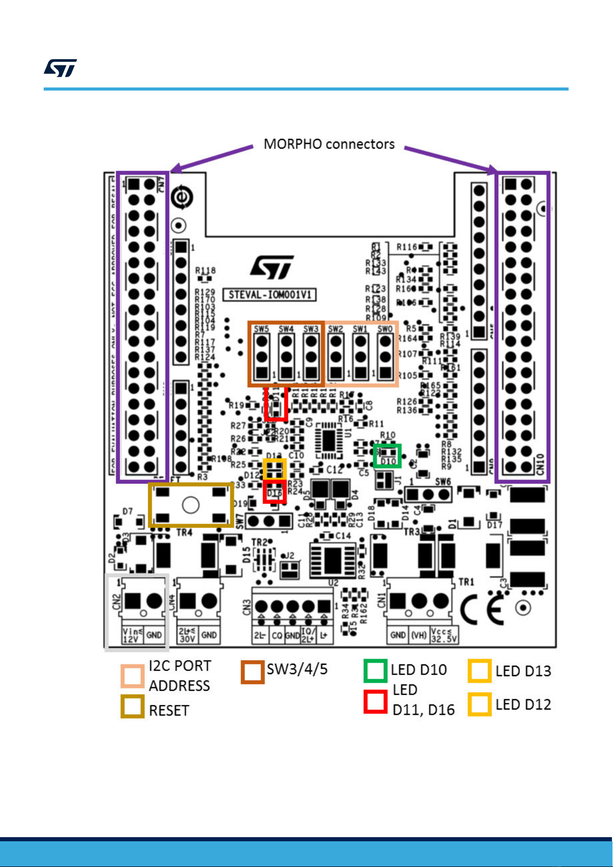
1. Default, via the CN1 pin (SW6, pins 2-3 closed):
–This is the same voltage rail that supplies the L6360 IO-Link transceiver and the IPS161H high side
switch are supplied through CN1.
2. An alternative power supply (SW6, pins 1-2):
Connector CN3 can be used to connect the STEVAL-IOM001V1 to a remote IO-Link device according to the
IO-Link specifications for port class A/type A and class B/Type B.
The board can supply the remote device through the L+ line, which can be controlled by the L+ switch in the
L6360 (ENL+ signal) IC or through the IPS161H (L+_ON signal). The CQ line of CN3 is directly connected to pins
CQO and CQI on the L6360 device.
By default (Type A, SW7 close 1-2), the DI/DQ line of the IO-Link cable is connected to the additional digital input
IQ on the L6360.
Alternatively (Type B, SW7 close 2-3), pin 2 of CN3 can supply the second L+ rail (typically used for actuators).
For Type B connections, CN4 is use to connect the power supply for 2nd L+ and 2nd ground.
Table 8. CN1, CN2, CN3, CN4 details
CONNECTOR PIN SIGNAL
CN1
1 GND
2Default (SW6 close2-3): connected to pin 3 of CN1.
Alternate (SW6 close1-2): separated supply for VH pin of L6360
3 Supply (≤32.5V) for L6360 and IPS161H
CN2
1 Alternative supply (between 7 and 12V) for STM32 Nucleo board
2 GND
CN3
1 IO-Link L+ supply rail for remote device.
2Default (Type A, SW7 close 1-2): IO-Link DI/DQ line.
Alternate (Type B SW7 close 2-3): IO-Link 2nd L+ supply rail.
3 GND
4 IO-Link CQ line.
5 2nd ground (reference of 2nd L+ supply rail), Type B only.
CN4
1 Input pin for 2nd L+ power supply.
2 Input pin for 2nd ground.
2.5 Protection features
The protection section implements reverse polarity protection and Electromagnetic compatibility (EMC) noise
protection according to the industrial standards IEC61000-4-2 (ESD), IEC61000-4-4 (Burst) and IEC61000-4-5
(Surge).
UM2414
Protection features
UM2414 - Rev 2 page 10/22

Figure 5. STEVAL-IOM001V1 expansion board power section components
Table 9. Protection device descriptions
Protection device Description Notes
TR1 VCC/VH supply surge pulse suppressor
D1 VCC/VH reverse polarity protection diode
D17 VCC/VH clamping for negative Surge Pulse protection
TR2 CQ, IQ and L+ lines surge suppressor.
D4 Schottky diodes with low VF clamp the disturbance applied to the lines in a reverse polarity
direction. Capable of conducting high surge current pulses to avoid high peak
current flow through the L6360 pins
D5
D3 VIN supply surge pulse suppressor Not mounted
D7 VIN Clamping for negative Surge Pulse protection Not mounted
D2 VIN reverse polarity protection diode Not mounted
TR4 2nd L+ supply surge pulse suppressor Not mounted
UM2414
Protection features
UM2414 - Rev 2 page 11/22

Protection device Description Notes
D15 2nd L+ Clamping for negative Surge Pulse protection Not mounted
D19 2nd L+ reverse polarity protection diode Not mounted
TR3 VH supply surge pulse suppressor Not mounted
D14 VH reverse polarity protection diode Not mounted
D18 VH clamping for negative Surge Pulse protection Not mounted
2.6 Powering and initializing the board
Follow the instructions below to start using the STEVAL-IOM001V1 IO-Link physical master evaluation board:
Step 1. Connect the STEVAL-IOM001V1 evaluation board to the NUCLEO-F446RE or NUCLEO-F401RE
development board through the morpho connectors.
Step 2. Connect the micro-USB cable between your computer and the STM32 NUCLEO development board
Set J5 to position “U5V”
Step 3. Download the STSW-IOM001 firmware onto the STM32 Nucleo microcontroller
The firmware is the user reference code to control the L6360 and can be freely downloaded from
www.st.com. You can use the STM32 ST-Link utility to load the firmware onto the STM32 Nucleo
board.
Step 4. Ensure that the STEVAL-IOM001V1 is configured as io-link port-1
Step 5. Connect the STEVAL-IOM001V1 to a 24 V power supply through CN1 pins 3 (+24V) and 1 (GND).
Step 6. Connect the load (or probes) on the CN3 pins 1 (L+), 2 (IQ), 3 (GND) and 4 (CQ).
Step 7. Use the dedicated graphic user interface (STSW-IOLINKGUI) to control the system.
ST offers a complete IO-Link master solution (physical layer and stack) with the P-NUCLEO-IOM01M1. The
STEVAL-IOM001V1 can be stacked with the P-NUCLEO-IOM01M1 to create a multi-port IO-Link master (up to
quad-port).
RELATED LINKS
2.3 IO-Link port configuration on page 8
2.4 Supply section on page 8
UM2414
Powering and initializing the board
UM2414 - Rev 2 page 12/22

3STEVAL-IOM001V1 schematic diagrams
Figure 6. STEVAL-IOM001V1 circuit schematic (1 of 4)
Vdd
4
U2
1
C/Qi
270
INCQ
680
10
OUT10
2
7
GND
JP2
4k7
D10
9
2
EN_CQ
1
R13
1
2
SW KEY-Y1011
D13
TR2
C14
U1
JP3
6NC6
R26
SW KEY-Y1011
JUMP
R28
5
3
L-
2
14
1
L6360
100nF
SPT01-335DEE
OUT11 11
IQ
16
SCL
2
1
0R29
R19
4
D11
OL-OFF
L+
2
VH
L- 21
STPS1L40M
270
270
SW2
NC5
5
1
SDA
JUMP
EN_L+
9
SDA
R20
8
STPS1L40M
3
1
SW KEY-Y1011
IQ
VH
3
Rbias
9
OUT9
4CoD
R18
YELLOW
L+_U2
R12
R27680
R15
R16
100nF
3
SW1
1
C13
3
C5 100nF
IRQ
2
OUTCQ
2
7
20
LED1 19
R32
1k
2 8 Sel
2
CQio
100nF
10k
2
L+_ON
VH
27
2
25
C/Qo 26
1
R17
10nFC10
R24
1
2
C7
1
Vdd
RST
1
D16 RED
1
1
R14
1
15
1
C6
OUTIQ
RESET
2
R11
3
RST
SCL
2
IRQ
NC12
1
J2
VCC_U2
L+_U1
10k
OUT I/Q
SDA
3
SA0
560pF
100nF
2
SW5
1
SW KEY-Y1011
270
C9
4K7
INCQ
SW KEY-Y1011
3DIAG
SW4
IN C/Qo
11
100nF
1
I/Q
2
1
Vdd
R31
D4
C8
1
J1
2
22
10
R34 68k (N.M.)
VCC_U1
R21
1
3
1
2
L+_U2
3
ENL+
RST
Vcc
1
13
2
C11
270
VCC_U1
15
SA0
1
24
3
2
IN1
2
L+_U1
270
3
SW0
560pF
VCC
GREEN
ENCQ
TAB
R30
Vdd
4
7
3k3
6
CQio
270
R22
Vdd
IRQ
Vcc
RED
R25
C12
ENL+
YELLOW
2
1k
18
5SA1
SA2
6
R33 1k
23
EP
1nF
4K7
SA0
124K 0,1%
SW3
8
OUT8
ENCQ
OUTCQ
12
2
R23
OUT C/Qi
12
D5
SW KEY-Y1011
2
R10
1
2
1
2
OUTIQ
270
SCL
VCC_U2
IPS161H
2
4K7
D12
13
L+
10k
NC1
1
LS HS
V+
A
V-
K
17
LED2
UM2414 - Rev 2 page 13/22
UM2414
STEVAL-IOM001V1 schematic diagrams

Figure 7. STEVAL-IOM001V1 circuit schematic (2 of 4): Arduino connectors
1
R9
100R(N.M.)
D9
CN9
IRQ
RST
A3 IRQ
L+_ON
INCQ
ENCQ
6
4
D6
5
4
100R
R162
D7
SDA
R143
D3
100R
R163
2
OUTCQ
6
2
D11
R3
D0
5
3
100R
R106
GND
D4
A2
SCL
100R(N.M.)
3
IOREF
3
OUTIQ
R1
CN6
1
100R(N.M.)
100R(N.M.)
7
R114
D2
A0
7
VIN
INCQ
10
A1
RST
SDA
2
INCQ
ENL+
8
100R(N.M.)
R104
100R(N.M.)
R117
R4
100R(N.M.)
CN5
1
100R(N.M.)
100R(N.M.)
8
D10
100R
R109
R5
R7
R115
SDA
R132
100R
100R(N.M.)
100R
9
4
3V3
OUTCQ
A5
100R(N.M.)
R8
SCL
RST
ENCQ
L+_ON
SCL
100R(N.M.)
8
R122
7
R118
100R(N.M.)
D5
R105
D1
100R
OUTCQ
3v3
100R
100R (N.M.)
)
AVDD
ENCQ
6
R2
R119
5V
D15
2
CN8
PB8
PC7
PB9
PA7
PB6
PA6
PA9
PA5
PB4
PB3
PB10
PA8
PA3
PA2
PB5
(PA10, SWO)
PA0
PA1
PC1
PA4
PB0
PC0
DEFAULT
DEFAULT
DEFAULT
(PORT #1)
(PORT #1)
DEFAULT
(PORT #1
DEFAULT
DEFAULT
(PORT #1)
DEFAULT (PORT #1
(PORT #1)
DEFAULT
(PORT#1)
(PORT #1)
(PORT #4)
(PORT #2)
R108
D8
100R (N.M.)
1
)
100R N.M.
R103
100R
A4
ENL+
NRST
R161
D14
5
100R(N.M.)
ENL+
GND
R111
3
5
4
6
D13
D12
UM2414 - Rev 2 page 14/22
UM2414
STEVAL-IOM001V1 schematic diagrams

Figure 8. STEVAL-IOM001V1 circuit schematic (3 of 4): ST morpho connectors
A5
R137
100R(N.M.)
10
L+_ON
100R(N.M.)
CON38
A0
ENCQ
6
A3
15
R139
27
R170
17
D0
8
32
D2
L+_ON
11
16
RST
3
1
14
AVDD
28
D3
23
D13
31
100R(N.M.)
R133
3
9
100R(N.M.)
OL-OFF
22
23
4
D12
100R(N.M.)
100R(N.M.)
R128
100R(N.M.)
R107
29
100R(N.M.)
24
25
34
4
8
100R(N.M.)
ENL+
21
30
NRST
IRQ
A4
28
29
35
100R(N.M.)
R124
12
13
D5
9
33
IOREF
5
D1
R136
100R(N.M.)
CN10
OUTIQ
GND D8
33
A1
R164
20
14
15
10
D14
6
26
27
A2
30
12
13
100R(N.M.)
ENCQ
R135
R129 100R(N.M.)
OUTCQ
D10
D7
R138
OUTIQ
OUTIQ
31
D11
100R(N.M.)
R126
37
7
19
21
D15
100R(N.M.)
7
19
11
R123
R134
RST
100R(N.M.)
36
17
D6
5V
32
24
37
PC2
PC13 (BLUE PB)
PA1
NC
PD2 SPI3_CS
PC1
PC3
PA14 (TCK)
PCPDA_RESET PA15
PB0
VDD
NC
(PC14, RCC_OSC32_IN)
(PC15, RCC_OSC32_OUT)
(PH0, RCC_OSC_IN)
(PH1, RCC_OSC_OUT)
PA0
PC11 SPI3_MISO
BOOT0
VBAT
PB7
PA13 (TMS)
SPI3_SCL PC10
PA4
SPI3_MOSI PC12
PA8
PB4
PA2
PB6
PA9
U5V
PC5
PA5
PB10
PB12
PB3
PC4
PC7
PA6
NC
PB13
PA12
PA7
PB5
PB9
PA10
PC8
NC
PB1
PB14
PC6
PB2
PC9
PA3
NC
PB15
PA11
(PORT #2)
36
D9
2
OUTCQ
ENL+
R116
20
100R(N.M.)
INCQ
IRQ
CN7
E5v0
3v3
16
35
VIN
2 1
5
25
CON38
R165
18
22
38
PC0
D4
18
26
34
38
NC
PB8
Figure 9. STEVAL-IOM001V1 circuit schematic (4 of 4): supply voltage
IQ
L+
3
1
100nF
SW7
2
CQio
2
3
1
2L+
CN2
1
SW KEY-Y1011
1
STPS1L60 (N.M.)
STPS1L60
1
MORSV-254-5P
4
2
2
1
L+
D2
2
SM15T33CA (N.M.)
CQio
D15
VIN
7 V-12 V NUCLEO supply voltage
IO-Link Master supply
voltage 18 V - 32.5 V
2
D7
BAT48JFILM
D19
2
1
1
SMAJ15CA
5
1
2
2
TR4
CN3
CN4
STPS2L60 (N.M.)
C15
2L+
D3
STPS1L60
VH not protected vs RPP
VCC
VH TR1
SM15T33CA
C1
4.7nF/3kV N.M.
TR3
SM15T33CA (N.M.)
C4
2.2uF/50V
C3
4.7nF/3kV N.M
CN1
1
2
3
C2
2.2uF/50V
SW6
2 1
SW KEY-Y1011
3
D14
21
STP S 1L60 (N.M.)
D18
2 1
STPS1L60 (N.M.)
D17
2 1
D1
21
STP S 2L60
EARTH
UM2414 - Rev 2 page 15/22
UM2414
STEVAL-IOM001V1 schematic diagrams

4Bill of materials
Table 10. STEVAL-IOM001V1 bill of materials
Item Q.ty Ref. Part/Value Description Manufacturer Order code
1 1 U1 IO-Link communication
master transceiver IC ST L6360TR
2 1 D10 Green LED AlGaInP OSRAM LG L29K-G2J1-24
3 2 C2, C4 2.2µF 50V
±10% X7R Murata GRM31C71H225KA88K
4 2 JP2, JP3 Drop Jumper - -
5 7 C5, C6, C7, C8,
C12, C14, C15
100nF 50V
±10% X7R TDK CGA3E2X7R1H104K080AA
6 1 C9 1nF 16V
±15% X7R WURTH 885012206034
7 1 C10 10nF 16V
±10% X7R Murata GRM188R71C103KA01D
8 2 C11, C13 560pF 50V
±10% X7R Multicomp MC0603B561K500CT
9 2 D11, D16 Red LED AlGaInP OSRAM LS L29K-G1 J2-1
10 2 D12, D13 Yellow LED 2.4V, 20mA
AlGaInP Kingbright KPG-0603SYC-TT
11 8
SW0, SW1, SW2,
SW3, SW4, SW5,
SW6, SW7
- 3-way, 1-row HARWIN M20-9990346
11a 8 Jumper shunt
connector - Jumper shunt connector ASSMANN WSW AKSPT/G GREY
12 9 R1, R2, R3, R4 R5,
R7, R8, R9, R162
100Ω 0.1W
±0.5% Panasonic ERJ3BD1000V
13 0
R34, R103, R104,
R105, R106, R107,
R108, R109, R111,
R114, R115, R117,
R118, R119, R122,
R123, R124, R126,
R128, R129, R132,
R133, R134, R135,
R136, R137, R138,
R139, R143, R161,
R162, R163, R164,
R165
- not mounted - -
14 3 R19, R32, R33 1kΩ 0.1W
±1% - TE Connectivity CRG0603F1K0
15 1 R11 124kΩ 0.1W
0.1% - TE Connectivity CPF0603B124KE1
16 8
R12, R13, R14,
R15, R16, R20,
R21, R22
270Ω 0.1W
±1% - Vishay CRCW0603270RFKEA
17 3 R17, R18, R31 10kΩ 0.1W
±1% - TE Connectivity CRG0603F10K
18 1 R30 3.3kΩ 0.1W
±1% - TE Connectivity CRG0603F3K3
UM2414
Bill of materials
UM2414 - Rev 2 page 16/22

Item Q.ty Ref. Part/Value Description Manufacturer Order code
19 2 R23, R24 680Ω 0.1W
±1% - Vishay CRCW0603680RFKEA
20 4 R10, R25, R26,
R27
4k7Ω 0.1W
±1% - ROHM MCR03EZPFX4701
21 1 R28 15Ω 0.1W
±1% - Vishay CRCW060315R0FKEA
22 1 R29 0Ω 0.1W ±1% - TE Connectivity CRG0603ZR
23 0 CN5 Not mounted 10-way, 1-row SAMTEC SSQ-110-04-F-S
24 0 CN6, CN9 Not mounted 8-way, 1-row SAMTEC SSQ-108-04-F-S
25 2 CN7, CN10 38-way, 2-row SAMTEC ESQ-119-24-T-D
26 0 CN8 Not mounted 6-way, 1-row SAMTEC SSQ-106-04-F-S
27 1 CN1 3-way, 1-row (L6360
supply) RS 790-1143
28 1 CN2 2-way, 1-row (STM32
NUCLEO supply) RS 790-1149
29 0 CN4 Not mounted 2-way, 1-row (Additional
supply 2L+) RS 790-1149
30 1 CN3 5-way, 1-row (connection
to IO-Link Slave) RS-Pro MB312-25405NIP
31 0 C1, C3
47nF 3kV
±10%
Not mounted
X7R Vishay HV2220Y472KXHATHV
32 1 TR1 Vcc (VH) TVS surge
suppressor ST SM15T33CA
33 0 TR3, TR4 Not mounted VH TVS surge suppressor ST SM15T33CA
34 1 TR2 IO-LINK LINE EMC
PROTECTION ST SPT01-335DEE
35 1 D1 VCC reverse polarity
protection 2A, 60V ST STPS2L60A
36 0 D14 Not mounted VH reverse polarity 1A,
60V ST STPS1L60ZF
37 0 D15 Not mounted 2L+ reverse polarity 2A,
60V ST STPS2L60A
38 1 D2 VIN reverse polarity
protection 0.35A, 40V ST BAT48JFILM
39 2 D4, D5
SURGE PULSE
PROTECTION 1.0A,
0.40V
ST STPS1L40M
40 1 D3 Vin EMC Suppressor
400W ST SMAJ15CA
41 2 D7, D17 Vcc, Vin Free Wheeling
diodes 1A, 60V ST STPS1L60ZF
42 0 D18, D19 Not mounted Vcc Free Wheeling Diode
1A, 60V ST STPS1L60ZF
43 1 RESET RESET BUTTON TE Connectivity 2-1437565-7
44 1 U2 External L+ Switch ST IPS161H
45 2 J1, J2 VCC and L+ connection
switches - -
UM2414
Bill of materials
UM2414 - Rev 2 page 17/22

Contents
1Hardware and software requirements ..............................................2
2STEVAL-IOM001V1 evaluation board overview .....................................3
2.1 Features ......................................................................3
2.2 Digital section .................................................................3
2.2.1 ST morpho connectors ....................................................5
2.2.2 I2C Port address .........................................................6
2.2.3 Reset button ............................................................7
2.2.4 LEDs..................................................................7
2.2.5 SW3, SW4 and SW5 digital switches .........................................7
2.3 IO-Link port configuration........................................................8
2.4 Supply section .................................................................8
2.5 Protection features ............................................................10
2.6 Powering and initializing the board ...............................................12
3STEVAL-IOM001V1 schematic diagrams...........................................13
4Bill of materials...................................................................16
Revision history .......................................................................18
UM2414
Contents
UM2414 - Rev 2 page 19/22

List of figures
Figure 1. STEVAL-IOM001V1 IO-Link physical master evaluation board ...................................1
Figure 2. STEVAL-IOM001V1 plus STM32 Nucleo board..............................................2
Figure 3. STEVAL-IOM001V1 expansion board digital interface components ................................4
Figure 4. Alternative power input sections for the STEVAL-IOM001V1 plus STM32 Nucleo ......................9
Figure 5. STEVAL-IOM001V1 expansion board power section components ................................ 11
Figure 6. STEVAL-IOM001V1 circuit schematic (1 of 4) .............................................. 13
Figure 7. STEVAL-IOM001V1 circuit schematic (2 of 4): Arduino connectors ............................... 14
Figure 8. STEVAL-IOM001V1 circuit schematic (3 of 4): ST morpho connectors ............................. 15
Figure 9. STEVAL-IOM001V1 circuit schematic (4 of 4): supply voltage ................................... 15
UM2414
List of figures
UM2414 - Rev 2 page 20/22
Table of contents
Other ST Motherboard manuals

ST
ST STM3210E-EVAL User manual

ST
ST EVB-LIV3F User manual

ST
ST STEVAL-IFS002V2 User manual

ST
ST STM32F401 Discovery User manual

ST
ST STEVAL-L6983IV1 User manual

ST
ST STMPE801 User manual

ST
ST EVAL-L9001 User manual

ST
ST STM32L4R9I User manual

ST
ST STEVAL-ILL009V1 Installation and operating instructions

ST
ST STEVAL-SP1ML915 User manual

ST
ST UM1509 User manual

ST
ST STM32H743I-EVAL User manual

ST
ST STUSB02E User manual

ST
ST STSW-STUSB002 User manual

ST
ST STM32 Nucleo-64 User manual

ST
ST STEVAL-ISB68RX User manual

ST
ST STM32F334 User manual

ST
ST EVALSP820-XS User manual

ST
ST STEVAL-IFS001V1 User manual

ST
ST STA333ML Installation and operating instructions