ST SPC584BADPT176S User manual

Introduction
The SPC584BADPT176S Rev.A evaluation board supports STMicroelectronics SPC584BxxE7, SPC584CxxE7 and
SPC58ECxxE7 microcontrollers in LQFP 176 package.
Figure 1. SPC584BADPT176S Rev.A
Picture is not contractual
SPC584BADPT176S Rev.A evaluation board
UM2756
User manual
UM2756 - Rev 1 - August 2020
For further information contact your local STMicroelectronics sales office.
www.st.com

1Overview
The SPC584BADPT176S mini module is an evaluation board supporting STMicroelectronics SPC584BxxE7,
SPC584CxxE7 and SPC58ECxxE7 microcontrollers in LQFP176 package.
The mini module is designed to be connected onto the SPC58xxMB motherboard, offering a mechanism for easy
customer evaluation of the supported devices, and to facilitate hardware and software development.
The mini module may be used as a stand-alone unit allowing access to the CPU, but no access to the I/O pins as
any motherboard peripherals.
Figure 2. Overview of SPC584BADPT176S mini module - top
UM2756
Overview
UM2756 - Rev 1 page 2/24

Figure 3. Overview of SPC584BADPT176S mini module - bottom
1.1 Package contents
An SPC584BADPT176S adapter package includes the following item:
• SPC584BADPT176S mini module
1.2 Supported devices
The SPC584BADPT176S mini module supports the following STMicroelectronics family of microcontrollers in
LQFP176 package:
• SPC584BxxE7
• SPC584CxxE7
• SPC58ECxxE7
UM2756
Package contents
UM2756 - Rev 1 page 3/24

2License agreement
The packaging of this evaluation board was sealed with a seal stating, “by breaking this seal, you agree to the
terms and conditions of the evaluation board license agreement, the terms and conditions of which are available
at http://www.st.com/ebla”. Upon breaking the seal, you and STMicroelectronics entered into the evaluation board
license agreement, a copy of which is also enclosed with the evaluation board for convenience.
Attention: This evaluation board only offers limited features for evaluating ST products. It has not been tested for use with
other products and is not suitable for any safety or other commercial or consumer application. This evaluation
board is otherwise provided “AS IS” and STMicroelectronics disclaims all warranties, express or implied,
including the implied warranties of merchantability and fitness for a particular purpose.
UM2756
License agreement
UM2756 - Rev 1 page 4/24

3Handling precautions
Please take care to handle the package contents in a manner such as to prevent electrostatic discharge.
Before the EVB is used or power is applied, please fully read the following sections on how to correctly configure
the board. Failure to correctly configure the board may cause irreparable component, MCU or EVB damage.
UM2756
Handling precautions
UM2756 - Rev 1 page 5/24

4Hardware description
4.1 Hardware features
The SPC584BADPT176S mini module board has the following features:
• Connector for external power supplies input (5.0 V, 3.3 V, 1.25 V) used in stand-alone mode
• Reset button with driver and led indicator
• Socket for device in eLQFP176 package with exposed pad down
• Debug ports:
– 38-pin Nexus Mictor connector for Nexus parallel interface
– 14-pin header connector for JTAG port
– 12-pin header connector for LFAST interface
• 40 MHz crystal main oscillator with jumpers to optionally disconnect it
• 8 MHz oscillator with jumpers to optionally disconnect it
• Clock input through SMA connector to optionally disconnect it
• 2 X SAMTEC QSH series, 240-way connector to connect mini module to motherboard
4.2 Hardware dimension
The mini module has the following dimensions:
• PCB area: 127 mm X 114.3 mm
• Top components height: 19.4 mm max
• Bottom components height: 3.5 mm max
• PCB thickness: 1.6 mm
UM2756
Hardware description
UM2756 - Rev 1 page 6/24

5Power and system configuration
5.1 Power supplies
When the mini module is plugged onto the motherboard, power is supplied directly by the motherboard. In this
setup, the external power supply input available on the mini module should NOT be used.
When the SPC584BADPT176S mini module is used as a stand-alone board, external power supplies must be
used (5.0 V, 3.3 V, 1.25 V).
The following jumpers are used to configure the power supply:
Table 1. Power configuration jumpers
Jumper Description Default Position
J1
VDD_HV_ADR voltage selenction - from
• 1-2 5.0V_LR
• 3-2 5.0V_SR
• 4-2 3.3V_SR
1-2 (5.0V_LR) Figure 4. SPC584BADPT176S top mini
module view - C2
J2
VDD_HV_ADV voltage selection - from
• 1-2 5.0V_LR
• 3-2 5.0V_SR
• 4-2 3.3V_SR
1-2 (5.0V_LR) Figure 4. SPC584BADPT176S top mini
module view - B2
J3
VDD_HV_JTAG voltage selection - from
• 1-2 5.0V_SR
• 3-2 3.3V_SR
1-2 (5.0V_SR) Figure 4. SPC584BADPT176S top mini
module view - B2
J6
VDD_HV_IO_MAIN voltage selection - from
• 1-2 5.0V_SR
• 3-2 3.3V_SR
1-2 (5.0V_SR) Figure 4. SPC584BADPT176S top mini
module view - B2
J7
VDD_HV_IO_FLEX voltage selection - from
• 1-2 5.0V_SR
• 3-2 3.3V_SR
1-2 (5.0V_SR) Figure 4. SPC584BADPT176S top mini
module view - B2
J45
Supply of the BALLAST circuit
• 1-2 VDD_HV_IO_MAIN
• 3-2 5.0_SR
1-2
(VDD_HV_IO_MAIN)
Figure 4. SPC584BADPT176S top mini
module view - A2
J40
VDD_LV voltage selection - from
• 1-2 BALLAST circuit
• 3-2 1.25V_SR
• 4-2 SMPS_REGULATOR_OUT
2-3 (1.25V_SR) Figure 4. SPC584BADPT176S top mini
module view - A3
UM2756
Power and system configuration
UM2756 - Rev 1 page 7/24

5.2 Port configuration
The following jumper need to configure the ports:
Table 2. Ports related jumpers
Jumper Description Default Position
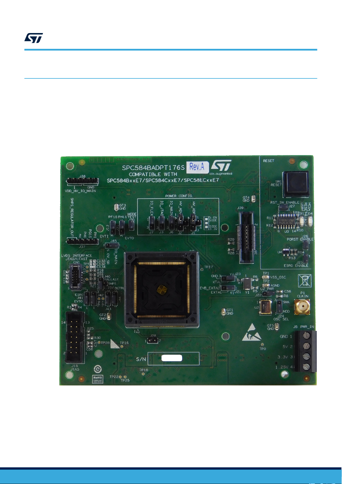
J30 TESTMODE settings Close Figure 4. SPC584BADPT176S top mini module view -
B2
J13
PH[12]/EVTI connection to QSH motherboard
connectors
• 1-2 PH12
• 3-2 EVTI
1-2 (PH12) Figure 4. SPC584BADPT176S top mini module view -
A2
J31
PJ[3]/EVTO connection to QSH motherboard
connectors.
• 1-2 PJ3 (allowed)
• 3-2 EVTO (reserved)
1-2 (PJ3) Figure 4. SPC584BADPT176S top mini module view -
A2
J42
PA8/TDI_TxDATA_N connection to QSH
motherboard connectors or LFAST
INTERFACE
Close 2-3 Figure 4. SPC584BADPT176S top mini module view -
A3
J43
PA9/TDO_RxDATA_P connection to QSH
motherboard connectors or LFAST
INTERFACE
Close 2-3 Figure 4. SPC584BADPT176S top mini module view -
A3
J44 PA14/RDY connection to QSH motherboard
connectors or Nexus parallel interface Close 2-3 Figure 4. SPC584BADPT176S top mini module view -
A3
J41
EVTO/ESR0 connection
Configuration 1-2 allowed, Configuration 2-3
Reserved.
Close 1-2 Figure 4. SPC584BADPT176S top mini module view -
A3
5.3 System clock configuration
The mini module supports the usage of crystal clock sources as well as external clock source:
Table 3. Clock configuration jumpers
Jumper Description Default Position
J21 40 MHz crystal clock source Enable
for pin EXTAL 1-2 (XT1 pin2) Figure 4. SPC584BADPT176S top mini module view -
C3
J23 40 MHz crystal clock source Enable
for pin XTAL 1-2 (XT1 pin1) Figure 4. SPC584BADPT176S top mini module view -
C3
J22 Enable 8 MHz oscillator power supply Open Figure 4. SPC584BADPT176S top mini module view -
D3
J24 External clock source from 8 MHz
oscillator or SMA connector
1-2 (8 MHz
oscillator)
Figure 4. SPC584BADPT176S top mini module view -
D3
UM2756
Port configuration
UM2756 - Rev 1 page 8/24

5.4 Reset circuit
The mini module supports different ways to reset the microcontroller.
To use and perform the reset driving there are different jumpers and switches:
Table 4. Reset configuration jumpers
Jumper Description Default Position
SW1 Reset push button Open Figure 4. SPC584BADPT176S top mini module view - D1
J27
Connect the external reset to the reset driver
for
ESR0 and PORST pins
Close Figure 4. SPC584BADPT176S top mini module view - D1
J25 Connect the external reset to ESR0 pin Close Figure 4. SPC584BADPT176S top mini module view - D2
J26 Connect the external reset to PORST pin Close Figure 4. SPC584BADPT176S top mini module view - D2
5.5 Test points
The mini module has several test points. Below all test point description:
Table 5. Test points
Test point Description Position
TP0 VDD_HV_IO_MAIN test point Figure 4. SPC584BADPT176S top mini module view - D4
TP1 VSS_OSC test point Figure 4. SPC584BADPT176S top mini module view - D3
TP2 AGND test point Figure 4. SPC584BADPT176S top mini module view - D3
TP3 JCOMP_RxDATA_N/PA[5] test point Figure 4. SPC584BADPT176S top mini module view - A2
TP4 TCK/PA[6] test point Figure 4. SPC584BADPT176S top mini module view - A2
TP5 TMS_TxDATA_P/PA[7] test point Figure 4. SPC584BADPT176S top mini module view - A3
TP6 TDI_TxDATA_N/PA[8] test point Figure 4. SPC584BADPT176S top mini module view - A3
TP7 TDO_RxDATA_P/PA[9] test point Figure 4. SPC584BADPT176S top mini module view - A3
TP16 PA[0] test point Figure 4. SPC584BADPT176S top mini module view - A4
TP17 PB8 Figure 4. SPC584BADPT176S top mini module view - C3
TP18 PE3 Figure 4. SPC584BADPT176S top mini module view - B4
TP22 J16A, QSH connector, pin10 test point Figure 4. SPC584BADPT176S top mini module view - A4
TP25 J16A, QSH connector, pin12 test point Figure 4. SPC584BADPT176S top mini module view - B4
TP28 J16A, QSH connector, pin11 test point Figure 4. SPC584BADPT176S top mini module view - A4
UM2756
Reset circuit
UM2756 - Rev 1 page 9/24

5.6 Connectors
The mini module has other connectors described in the below table.
Table 6. Other connectors
Connectors Description Position
J20 12-pin header connector for SIPI interface Figure 4. SPC584BADPT176S top mini module view - C2
J18 14-pin header connector for JTAG port Figure 4. SPC584BADPT176S top mini module view - A4
CN1 12-pin SAMTEC connector for JTAG/LFAST
LVDS interface Figure 4. SPC584BADPT176S top mini module view - A3
J36, J37 DC-DC Regulator Module Figure 4. SPC584BADPT176S top mini module view - A1/A2
J16, J17 2 X SAMTEC QSH series, 240-way connector to
connect mini module to motherboard Figure 5. SPC584BADPT176S bottom mini module view
UM2756
Connectors
UM2756 - Rev 1 page 10/24

6Layout overview
Figure 4. SPC584BADPT176S top mini module view
1
2
3
4
ABCD
UM2756
Layout overview
UM2756 - Rev 1 page 11/24

Figure 5. SPC584BADPT176S bottom mini module view
1
2
3
4
ABCD
UM2756
Layout overview
UM2756 - Rev 1 page 12/24

7BOM
Table 7. BOM
Item Qty Reference Manufacturer code Value Part description
1 1 CN1 TFM-105-02-L-D-WT
Samtec
TFM-105-02-L-D-
WT
Samtec 5x2 TFM connector - 1.27
mm pitch - - with weld tabs
2 11
C1, C3, C5, C7, C16,
C18, C20, C22, C24,
C58, C103
GCM188R71H104KA57D 100 nF Mult. cer. cap. 50V 0603
3 14
C2, C4, C6, C8, C17,
C19, C21, C23, C25,
C39, C42, C45, C48,
C104
GCM188R71H103KA37D 10 nF Mult. cer. cap. 50V 0603 (Automotive
Series)
4 5 C14, C15, C100, C101,
C102 GRM31CR71H475KA12L 4.7 uF Mult. cer. cap. 50V 1206
5 1 C28 GRM188R71E105KA12D 1 uF Mult. cer. cap. 25V 0603
6 1 C29 DNM Mult. cer. cap. 50V 0603 (Automotive
Series) - not mounted
7 4 C38, C41, C44, C47 GCM188R71H473KA55D 47 nF Mult. cer. cap. 50V 0603
8 4 C40, C43, C46, C49 C0603C225K4PAC 2.2 uF Mult. cer. cap. 16V 0603
9 2 C56, C57 DNM Mult. cer. cap. 50V 0603 - not
mounted
10 3 C121, C125, C127 GCM21BR71C225KA64L 2.2 uF Mult. cer. cap. 16V 0805 - Automotive
Series
11 4 C123, C124, C126,
C128 DNM Mult. Cer. cap. 50V 0603 - do not
mount
12 2 C132, C133 DNM Mult. cer. cap. 50V 0603 - not
mounted
13 1 C134 C0603C270J5GAC 27 pF Mult. cer. cap. 50V 0603
14 1 D1 HSMY-C150 Yellow Led diode yellow 1206
15 1 D4 HSMS-C150 Red Led diode red 1206
16 7 TP1, GT1, TP2, GT2,
GT3, GT4, GT5 TEST POINT SMD PCB test point
17 1 J1, J2 STRIP3+1PM Strip male 3+1 pin - see mech part
18 3
J3, J6, J7, J13, J21,
J23, J24, J31, J41, J42,
J43, J44, J45
STRIP 2 mm
Male strip 3 poles, single row,
vertical, golden, pitch 2 mm - see
mech parts
19 1 J5 31072104 METZ 31072104 CONN METZ CONNECT 4 POLI 16A
31072104
20 2 J16, J17 SAM-QSH12001LDA Samtec
QSH-120-01-L-D-A
Samtec 0.5mm pitch High Speed
Socket
21 1 J18 N2514-6002RB N2514-6002RB 3M conn flat male 14 pins, straight -
pitch 2.54 mm
22 0 J22 (included in J3) STRIP 2 mm
Male strip 2 poles, single row,
vertical, golden, pitch 2 mm - see
mech parts
23 0 J25, J26, J27, J30
(included in J3) STRIP 2 mm
Male strip 2 poles, single row,
vertical, golden, pitch 2 mm - see
mech Parts
UM2756
BOM
UM2756 - Rev 1 page 13/24

Item Qty Reference Manufacturer code Value Part description
24 1 J28 STRIP2PM Strip male 2 pin
25 0 J36, J37 STRIP6PM Strip male 6 pin
26 1 J39 5767054-1 5767054-1 Conn female 38 Pin, 180°, MICTOR -
GND
27 0 J40 (included in J3) STRIP 2mm
Male Strip 4 poles, single row,
vertical, golden, pitch 2 mm - See
mech parts
28 1 P1 SMA-J-P-H-ST-TH1 CON 1 SMA Female RF SMA 180°
29 1 Q1 NJD2873T4G NJD2873 NPN plastic power transistor DPAK
30 8 R1, R2, R7, R15, R18,
R19, R21, R22 0R Resistor 1/10W 1% 0603
31 4 R3, R26 DNM Resistor 1/10W 1% 0603 - not
mounted
32 3 R4, R9, R27 CR1J10KF-MR 10K Resistor 1/10W 1% 0603
33 2 R5, R6 DNM Resistor 1/10W 1% 0603 - not
mounted
34 1 R8 100R Resistor 1/10W 1% 0603
35 2 R10, R12 CRCW0603560RFKEA 560R Resistor 1/10W 1% 0603
36 3 R11, R13, R14 4K7 Resistor 1/10W 1% 0603
37 1 R16 DNM Resistor 1/10W 1% 0805 - do not
mount
38 1 R17 DNM Resistor 1/10W 1% 0603 - not
mounted
39 4 R20, R23, R25, R30 DNM Resistor 1/10W 1% 0603 - not
mounted
40 2 R28, R29 CR1J10KF-MR 10K Resistor
41 1 SW1 Pushbutton Pushbutton NO B6110-0
42 12
TP3, TP4, TP5, TP6,
TP7, TP16, TP17, TP18,
TP22, TP25, TP28, TP0
TEST POINT Testpoinr SMD - ignore
43 1 U1 eQFP176(A0A4) - YAMAICHI
IC357-1764-168P-2
44 1 U2 ECS-3953M-080-BN-TR 8 MHz Hybrid quartz osc ECS 3953M
45 1 U3 74LVC125AMTR 74LVC125AMTR I.C. low voltage CMOS quad bus
buffers - SO14
46 1 U4 74V1G08STR 74V1G08STR CMOS AND gate
47 1 Y1 NX5032GA 40 MHZ Quartz 40MHz NX5032GA XTAL
NDK
48 1 CSSG20170421 R.0 MINIMODULE SPC584BADPT176S-CHORUS 2M
EQFP176
49 2 J1, J2 Bridge 2 pins female 2.54 mm pitch
50 19
J3, J6, J7, J13, J21,
J23, J24, J31, J41, J42,
J43, J44, J45, J22, J25,
J26, J27, J30, j40
Bridge 2 pins female 2 mm pitch
UM2756
BOM
UM2756 - Rev 1 page 14/24

8Schematics
Figure 6. Microcontroller power
separate ground for OSC & AGND
For layout: Check layout consideration
document for ground connection of
VSS_HV_ADR/V pins
GND Test points
DNP
the rmal plane ,
po wer 2W/ 3W
AS CLOSE AS POSSIBLE TO MCU
DEFAULT CLOSED 1-2
GND GND
VSS_OSC
VSS_OSC
AGND
AGND
GND
5.0V_SR
GND
3.3V_SR1.25V_SR
5.0V_LR 5.0V_SR
3.3V_SR
GND
VDD_HV_IO_MAIN
VDD_HV_IO_JTAG
GND
VDD_HV_IO_FLEX
AGND
AGND
AGND
VSS_OSC
GND GND GND GND GND
GND
GND GND GND GND
VDD_HV_IO_MAIN
VDD_LV
GND
GND GND
GND
GND
VDD_HV_IO_MAIN
5.0V_SR
1.25V_SR
SMPS_REGULATOR_OUT
C14
4.7uF
50V
1206
X7R
C42
10nF
X7R
50V
R1
0R
R15
0R C123
DNP
C1
100nF
50V
0603
X7R
C28
1uF
25V
X7R
0603
J1
STRIP3+1PM
2
1
3
4
C47
47nF
X7R
50V
C121
2.2uF
16V
0805
X7R
SPC584BADPT176S eQFP176
POWER PINS
ADC
OSC & JTAG (3.3V OR 5V)
FLASH DECOUPLING
I/O (3.3V-5V)
MCU CORE LOGIC (1.25V)
U1A
SPC58NE84_176ELQFP
VDD_HV_ADR_S 52
VSS_HV_ADR_S
51
VDD_HV_ADV 54
VSS_HV_ADV
53
VDD_LV1 24
VDD_LV2 68
VDD_LV3 100
VDD_LV4 123
VDD_HV_IO_MAIN1 25
VDD_HV_IO_MAIN2 69
VDD_HV_IO_MAIN3 99
VSSOSC
101 VDD_HV_JTAG_OSC 104
VDD_HV_IO_MAIN4 139
VDD_HV_IO_MAIN5 171
VDD_HV_FLA 154
EPAD
177
BCTRL / PM[15] 153
VDD_HV_IO_FLEX 165
C43
2.2uF
X5R
16V
C15
4.7uF
50V
1206
X7R
C20
100nF
50V
0603
X7R
C3
100nF
50V
0603
X7R
C127
2.2uF
X7R
C48
10nF
X7R
50V
C6
10nF
50V
0603
X7R
C2
10nF
50V
0603
X7R
J6
STRIP 2m m
1
2
3
C125
2.2uF
X7R
C21
10nF
50V
0603
X7R
C49
2.2uF
X5R
16V
C4
10nF
50V
0603
X7R
C128
DNP
C7
100nF
50V
0603
X7R
C24
100nF
50V
0603
X7R
R16
DNP
J2
STRIP3+1PM
2
1
3
4
Q1
NJD2873
D-PAK
B
E C
C22
100nF
50V
0603
X7R
C8
10nF
50V
0603
X7R
C100
4.7uF
50V
1206
X7R
C38
47nF
X7R
50V
C25
10nF
50V
0603
X7R
GT1
1
C44
47nF
X7R
50V
R2
0R
GT2
1
C39
10nF
X7R
50V
C23
10nF
50V
0603
X7R
J45
STRIP 2m m
1
2
3
C45
10nF
X7R
50V
C126
DNP
GT3
1
C29
10nF
50V
0603
X7R
C40
2.2uF
X5R
16V
C103
100nF
50V
0603
X7R
C46
2.2uF
X5R
16V
GT4
1
J40
STRIP 2m m
2
1
3
4
C16
100nF
50V
0603
X7R
J5
METZ 31072104
1
2
3
4
C101
4.7uF
50V
1206
X7R
J3
STRIP 2m m
1
2
3
J7
STRIP 2m m
1
2
3
GT5
1
TP1
1
C104
10nF
50V
0603
X7R
C17
10nF
50V
0603
X7R
C5
100nF
50V
0603
X7R
C18
100nF
50V
0603
X7R
C41
47nF
X7R
50V
C124
DNP
TP2
1
C19
10nF
50V
0603
X7R
C102
4.7uF
50V
1206
X7R
TP0
VDD_HV_ADV
VDD_HV_IO_MAIN
VDD_HV_FLA
VDD_HV_ADR
VDD_HV_IO_JTAG
VDD_HV_IO_FLEX
VDD_LV
UM2756 - Rev 1 page 15/24
UM2756
Schematics

Figure 7. Microcontroller I/O
Port pins and reset signal
are routed to motherboard.
High speed signals are not
routed to mother board, but have
test points to connect to test
on mother board connector
EVT signals are connected to optional
jumper to be routed to mother board.
DNP
FCCU
ADDED PA8 PA9 PA14 MOTHERBOAR D
CONNECTION S
GND
5.0V_SR
JCOMP_RxDATA_N(pg4)
TCK
(pg4)
TMS_TxDATA_P(pg4)
PA[0..15]
(pg6)
PC[0..15](pg6)
PE [0..15](pg6)
PI[0..15](pg6)
PG [0..15](pg6)
PB [0..15] (pg6)
PD[0..15] (pg6)
PF[0..15] (pg5,6)
EVTI (pg4)
PH[0..15] (pg6)
PJ[0..4] (pg6)
EV TO (pg4)
PK[0..14] (pg6)
EXTAL (pg5)
XTAL(pg5)
PORST (pg4,5)
PM[0..15] (pg6)
PL8 (pg6)
PH12
PJ3
TDI_TxDATA_N(pg4)
PA8
TDO_RxDATA_P(pg4)
PA9
PA14
RDY
J44
STRIP 2mm
1
2
3
TP4
J28
STRIP2PM
1 2
TP5TP3
J31
STRIP 2mm
1
2
3
TP6
TP16
J30
STRIP 2mm
12
TP7
R27
10K
TP17
SPC584BADPT176S eQFP176
SIGNALS
U1B
SPC58NE84_176ELQ F P
PC [9]
3PC [8]
4PC [7]
5PC [6]
6PC [5]
7PC [4]
8PC [3]
9PC [2]
11 PC [1]
12 PC [0]
13
PE[0]
14
PE[1]
15
PE[2]
16
PE[3]
19
PE[4]
20
PE[15]
59 PE[14]
60 PE[13]
62
PF[1] 74
PF[0] 75
PA [3]
82
PF[6] 84
PF[7] 85
PJ[0] 86
PJ[1] 87
PA [15]
88
PJ[2] 89
PF[8] 90
PJ[3] 91
PJ[4] 92
PH[5] 93
PH[6] 94
PF[9] 95
PF[10] 96
PF[11] 97
PF[12] 98
PF[13] 107
PA [14]
110
PA [8]
111 PA [7]
112
PA [9]
113
PA [5]
114
PA [6]
115
PF[14] 116
PH[11] 117
TESTMODE 118
PA [4]
120
PORST 121
PE[5]
126
PE[6]
127
PE[7]
128
PE[8]
131
PE[9]
132
PA [2]
133 PA [1]
134
PA [12]
135
PA [13]
136
PA [0]
137
PH[0] 140
PH[1] 141
PA [10]
142
PA [11]
143
PH[2] 144
PE[10]
145
PE[11]
146
PH[3] 147
PH[4] 148
PH[10] 149
PH[9] 150
PH[8] 151
PH[7] 152
PE[12]
160
PC [15]
161 PC [14]
162 PC [13]
163 PC [12]
166 PC [11]
167 PC [10]
168
PM[0] 169
PM[2] 170
PH[14] 172
PF[3] 173
PF[2] 174
PH[13] 175
PH[12] 176
PF[15] 119
EXTAL 102
XTAL 103
PB [0] 67
PB [1] 66
PB [2] 65
PB [3] 64
PB [4] 61
PB [5] 36
PB [6] 46
PB [7] 45
PB [8] 81
PB [9] 80
PB [10] 79
PB [11] 78
PB [12] 35
PB [13] 34
PB [14] 33
PB [15] 32
PI[0]
37
PI[1]
38
PI[2]
39
PI[3]
40
PI[4]
41
PI[5]
42
PI[6]
47
PI[7]
48
PI[8]
22
PI[9]
23
PI[10]
73
PI[11]
72
PI[12]
71
PI[13]
70
PI[14]
105
PI[15]
106
PD[0] 157
PM[4] 158
PD[2] 155
PD[1] 156
PD[4] 129
PD[5] 130
PD[6] 109
PD[7] 108
PD[8] 83
PD[9] 76
PD[10] 77
PD[11] 63
PD[12] 17
PD[13] 18
PD[14] 1
PD[15] 2
PG [0]
21
PG [1]
28
PG [2]
29
PG [3]
30
PG [4]
31
PG [5]
43
PG [6]
44
PG [7]
49
PG [8]
50
PG [9]
55
PG [10]
56
PG [11]
57
PG [12]
58
PG [13]
124
PG [14]
125
PG [15]
138
POS-PIN-1
178
POS-PIN-2
179
PK[0] 26
PK [1] 27
PM[14] 122
PM[6] 159
PK[14] 164
PL
[8] 10
J13
STRIP 2mm
1
2
3
J43
STRIP 2mm
1
2
3
R26
10K
J42
STRIP 2mm
1
2
3
TP18
PA0
PA1
PA2
PA3
PA4
PA10
PA11
PA12
PA13
PA15
PC0
PC1
PC2
PC3
PC4
PC5
PC6
PC7
PC8
PC9
PC10
PC11
PC12
PC13
PC14
PC15
PE0
PE1
PE2
PE3
PE4
PE5
PE6
PE7
PE8
PE9
PE10
PE11
PE12
PE13
PE14
PE15
PA_9
JCOMP_RxDATA_N
TCK
TMS_TxDATA_P
PA_8
PA_14
PG0
PG1
PG2
PG3
PG4
PG5
PG6
PG7
PG8
PG9
PG10
PG11
PG12
PG13
PG14
PG15
PI0
PI1
PI2
PI3
PI4
PI5
PI6
PI7
PI8
PI9
PI10
PI11
PI12
PI13
PI14
PI15
PD6
PD7
PF13
PJ0
PJ1
PJ2
PJ_3
PJ4
PB0
PB1
PB2
PB3
PB4
PB5
PB6
PB7
PB9
PB10
PB11
PB12
PB13
PB14
PB15
PD0
PD1
PD2
PD4
PD5
PD8
PD9
PD10
PD11
PD12
PD13
PD14
PD15
PF0
PF1
PF2
PF3
PF6
PF7
PF8
PF9
PF10
PF11
PF12
PF14
PH0
PH1
PH2
PH3
PH4
PH5
PH6
PH7
PH8
PH9
PH10
PH11
PH_12
PH13
PH14
PK0
PK1
PK14
XTAL
EXTAL
PORST
PM0
PM2
PM4
PM6
PM14
PB8
PF15
PH_12
PJ_3
PB11
PC2
PA_8
PA_9
PA_14
UM2756 - Rev 1 page 16/24
UM2756
Schematics

Figure 8. JTAG, JTAG LFAST and Nexus
Place CAPS as close to
connector pins as
possible but do NOT fit
caps at board assembly.
JTAG Connector
(VSS)
(VSS)
(VSS)
(VSS)
TDI, TDO, TCK, TMS & JCOMP are not connected to
daughter card.
PORST, ESR0, EVTI and EVTO are connected to daughtercard
EVTI_0/EVTO_0
PIN 138
(smps_pm os0)
PIN 140
(smps_vlx)
PIN 141
(smps_nm os1)
Previson eiger DC-DC regulato r
DNP
DNP
DNP
DNP
10 Pin Versio n
Nexus level 3+ support
VDD_HV_IO_JTAG
GND
GND
VDD_HV_IO_JTAG
VDD_HV_IO_MAIN
GND
GND
GND
GND
GND
VDD_HV_IO_JTAG
VDD_HV_IO_JTAG
VDD_HV_IO_JTAG
GND
GND
VDD_HV_IO_MAIN
VDD_HV_IO_MAIN
GND
TDI
TDO
TCK(pg3)
)3gp( ITVE
JCOMP
TMS
PORST
(pg3,5)
PORST
EVTO(pg3)
SMPS_REGULATOR_OUT
PH[0..15](pg3,6)
PG[0..15](pg3,6)
TMS_TxDATA_P(pg3) TDI_TxDATA_N (pg3)
TDO_RxDATA_ (pg3)
JCOMP_RxDATA_N
(pg3)
EVTI(pg3)
EVTO
(pg3)
ESR0(pg3,5)
TCK (pg3)
PORST (pg3,5)
TDI TDO
JCOMP TMS
TDO(pg4,6)
TCK(pg4,6)
TMS
(pg4,6)
TDI
(pg4,6)
JCOMP(pg4,6)
PORST
(pg4,5)
PJ[0..4]
(pg6)
PC[0..15]
(pg6)
PE[0..15](pg6)
PI[0..15](pg6)
PB[0..15](pg6) RDY
R29 10K
R20
DNP
R4
10K
J41
STRIP 2mm
1
2
3
R30
DNP
R3
10K
C134
27pF
0603
R17 100R
CN1
SAMTEC TFM-105-02-L-D-WT
1 2
3 4
5 6
7 8
9 10
11
12
J18
N2514-6002RB
12
34
65
7 8
910
11 12
13 14
R19
0R
C56 47nF
C132 DNP0603
J36
STRIP
2
1
3
4
5
6
R18
0R
R23
DNP
J39
5767054-1
NC1
1
NC2
3
MDO09
5
VSTBY
37 ToolIO0
35 VBatt2
33 VBatt1
31 ToolIO1
29 TDET/WDTC
27 RSTOUT
25 MDO11
23 JCOMP
21 TDI
19 TMS
17 TCK
15 MDO10
13 TDO
11 RSTIN
9BootCFG
7
NC3 2
NC4 4
CLKOUT 6
MSEO0 38
MSEO1 36
MCKO 34
EVTO 32
MDO0 30
MDO1 28
MDO2 26
MDO3 24
MDO4 22
MDO5 20
MDO6 18
MDO7 16
RDY 14
VTREF 12
EVTI 10
MDO08 8
GND1 39
GND2 40
GND3 41
GND4 42
GND5 43
C133 DNP0603
R28 10K
C57 47nF
R22
0R
J37
STRIP
2
1
3
4
5
6
R25
DNP
R21
0R
EVTI
TDO
TCK
TMS
TDI
JCOMP
TMS
JCOMP
PORST
EVTO
PG15
PH1
PH0
PB14
PH10
PJ0
RDY
PE3PJ1
PJ2
PH6
PI10
PI11
PI12
PI13
PI0
PB5
PB12
PB13
PC1
PH12
PJ3
PB15
JTAG/LFAST LVDS INTERFACE
JTAG interface
UM2756 - Rev 1 page 17/24
UM2756
Schematics

Figure 9. Clock and reset circuit
External oscillator
Reset circuit
External clock input
Note - External 3.3V
regulator MUST be
enabled when using
oscillator module
SMA style
Connector
Note - Internal
Pull-Up on Pin 1
Loop Controlled Pierce
Oscillator Circuit
(MCU Crystal Input)
(MCU Crystal Output)
Connect XTAL jumper to GND when driving EXTAL from
Oscilaltor Module or External Source (PLL Bypass
Mode)
REMOVE XTAL jumper when driving EXTAL from
Oscillator Module or External Source (PLL Enabled)
MCU RESET LED
USR RESET LED
Reset-In
Disable
GND
GND
3.3V_SR
VSS_OSC
GND
GND
GND
VDD_HV_IO_MAIN
VDD_HV_IO_MAIN
GND
GND
GND
VDD_HV_IO_MAIN
VDD_HV_IO_MAIN
EXTAL (pg3)
XTAL(pg3)
EVB-EXTAL
RST-SW (pg6)
ESR0 (pg3,5)
PORST (pg3,5)
EVB-EXTAL
R10 560R
D4
Red
R5
DNP
R11
4K7
J21
STRIP 2mm
1
2
3
R12 560R
R6
DNP
U3C
74LVC125AMTR
9 8
10
R14
4K7
J27
STRIP 2mm
1 2
J22
STRIP 2mm
12
VCC
GND
U3A
74LVC125AMTR
23
14
1
7
U3B
74LVC125AMTR
5 6
4
GND
VCC
U4
MC74HC1G08DTT1G
1
2
4
53
P1
1
2
4 3
5
D1 Yellow
R7 0R
SW1
Pushbutton
R8 100R
C58 100nF
J25
STRIP 2mm
12
CLK
OUT
VDD
GND
OE
8MHz
U2
42
31
J26
STRIP 2mm
1 2
J24
STRIP 2mm
1
2
3
R13
4K7
R9 10K
J23
STRIP 2mm
1
2
3
Y1
40MHZ
1 2
OSC-MOD
EVB-EXTAL
EXTAL-SMA
EXTAL
XTAL
EVB-EXTAL
ESR0
PORST
RST-MCU
RST-SW
UM2756 - Rev 1 page 18/24
UM2756
Schematics

Figure 10. Board connector
PortE PortF PortG PortH PortIPortC PortJ
PortA PortB PortD
PortJ PortM
NEW CONNECTIONS
ADDED PD6 PD7 PF13 CONNECTIONS TO MOTHERBOARD
REMOVED RELATIVE TESTPOINTS FROM MOTHERBOARD CONNECTORS
GND
3.3V_S R1.25V_SR 5.0V_LR5.0V_SR VDD_HV_IO_MAIN
GND
GND
VDD_HV_IO_FLEX
PF[0..15](pg4,6) PG [0..15]
(pg4) PI[0..15](pg4)PC[0..15](pg4) PJ[0..4](pg4)PA[0..15]
(pg4) PB [ 0..15]
(pg4) PD[0..15 ]
(pg4) PE [0..15](pg4)
RST-SW(pg7)
PH[0..15](pg4)
PL8(pg2)
PK [0..14]
(pg4) PM[0..15]
(pg4)
J17A
SAMT EC
QSH-120-01-L-D-A
11
33
55
77
99
11 11
13 13
15 15
17 17
19 19
21 21
23 23
25 25
27 27
29 29
31 31
33 33
35 35
37 37
39 39
41 41
43 43
45 45
47 47
49 49
51 51
53 53
55 55
57 57
59 59
61 61
63 63
65 65
67 67
69 69
71 71
73 73
75 75
77 77
79 79
81 81
83 83
85 85
87 87
89 89
91 91
93 93
95 95
97 97
99 99
101 101
103 103
105 105
107 107
109 109
111 111
113 113
115 115
117 117
119 119
2
24
46
68
810
10 12
12 14
14 16
16 18
18 20
20 22
22 24
24 26
26 28
28 30
30 32
32 34
34 36
36 38
38 40
40 42
42 44
44 46
46 48
48 50
50 52
52 54
54 56
56 58
58 60
60 62
62 64
64 66
66 68
68 70
70 72
72 74
74 76
76 78
78 80
80 82
82 84
84 86
86 88
88 90
90 92
92 94
94 96
96 98
98 100
100 102
102 104
104 106
106 108
108 110
110 112
112 114
114 116
116 118
118 120
120
TP28
J16B
SAMTEC QSH-120-01-L-D-A
SH1
SH1
SH2
SH2
SH3
SH3
SH4
SH4
SH5
SH5
SH6
SH6
SH7
SH7
SH8
SH8
SH9 SH9
121
121
123
123
125
125
127
127
129
129
131
131
133
133
135
135
137
137
139
139
141
141
143
143
145
145
147
147
149
149
151
151
153
153
155
155
157
157
159
159
161
161
163
163
165
165
167
167
169
169
171
171
173
173
175
175
177
177
179
179
181
181
183
183
185
185
187
187
189
189
191
191
193
193
195
195
197
197
199
199
201
201
203
203
205
205
207
207
209
209
211
211
213
213
215
215
217
217
219
219
221
221
223
223
225
225
227
227
229
229
231
231
233
233
235
235
237
237
239
239
SH16 SH16
SH15 SH15
SH14 SH14
SH13 SH13
SH12 SH12
SH11 SH11
SH10 SH10
122 122
124 124
126 126
128 128
130 130
132 132
134 134
136 136
138 138
140 140
142 142
144 144
146 146
148 148
150 150
152 152
154 154
156 156
158 158
160 160
162 162
164 164
166 166
168 168
170 170
172 172
174 174
176 176
178 178
180 180
182 182
184 184
186 186
188 188
190 190
192 192
194 194
196 196
198 198
200 200
202 202
204 204
206 206
208 208
210 210
212 212
214 214
216 216
218 218
220 220
222 222
224 224
226 226
228 228
230 230
232 232
234 234
236 236
238 238
240 240
TP25
J17B
SAMT EC
QSH-120-01-L- D-A
SH1 SH1
SH2 SH2
SH3 SH3
SH4 SH4
SH5 SH5
SH6 SH6
SH7 SH7
SH8 SH8
SH9
SH9
121 121
123 123
125 125
127 127
129 129
131 131
133 133
135 135
137 137
139 139
141 141
143 143
145 145
147 147
149 149
151 151
153 153
155 155
157 157
159 159
161 161
163 163
165 165
167 167
169 169
171 171
173 173
175 175
177 177
179 179
181 181
183 183
185 185
187 187
189 189
191 191
193 193
195 195
197 197
199 199
201 201
203 203
205 205
207 207
209 209
211 211
213 213
215 215
217 217
219 219
221 221
223 223
225 225
227 227
229 229
231 231
233 233
235 235
237 237
239 239
SH16
SH16
SH15
SH15
SH14
SH14
SH13
SH13
SH12
SH12
SH11
SH11
SH10
SH10
122
122 124
124 126
126 128
128 130
130 132
132 134
134 136
136 138
138 140
140 142
142 144
144 146
146 148
148 150
150 152
152 154
154 156
156 158
158 160
160 162
162 164
164 166
166 168
168 170
170 172
172 174
174 176
176 178
178 180
180 182
182 184
184 186
186 188
188 190
190 192
192 194
194 196
196 198
198 200
200 202
202 204
204 206
206 208
208 210
210 212
212 214
214 216
216 218
218 220
220 222
222 224
224 226
226 228
228 230
230 232
232 234
234 236
236 238
238 240
240
TP22
J16A
SAMTEC QSH-
120-01-L-D-A
1
1
3
3
5
5
7
7
9
9
11
11
13
13
15
15
17
17
19
19
21
21
23
23
25
25
27
27
29
29
31
31
33
33
35
35
37
37
39
39
41
41
43
43
45
45
47
47
49
49
51
51
53
53
55
55
57
57
59
59
61
61
63
63
65
65
67
67
69
69
71
71
73
73
75
75
77
77
79
79
81
81
83
83
85
85
87
87
89
89
91
91
93
93
95
95
97
97
99
99
101
101
103
103
105
105
107
107
109
109
111
111
113
113
115
115
117
117
119
119
22
44
66
88
10 10
12 12
14 14
16 16
18 18
20 20
22 22
24 24
26 26
28 28
30 30
32 32
34 34
36 36
38 38
40 40
42 42
44 44
46 46
48 48
50 50
52 52
54 54
56 56
58 58
60 60
62 62
64 64
66 66
68 68
70 70
72 72
74 74
76 76
78 78
80 80
82 82
84 84
86 86
88 88
90 90
92 92
94 94
96 96
98 98
100 100
102 102
104 104
106 106
108 108
110 110
112 112
114 114
116 116
118 118
120 120
PA8
PA14
PI2
PI4
PI6
PI0
PI8
PI10
PI12
PI14
PG 2
PG0
PG 4
PG 6
PG 8
PG1 0
PG1 2
PG1 4
5.0V_SR
PE 2
PE 4
PE 6
PE 8
PE 0
PE10
PE12
PE14
1.25V_SR
PC0
PC2
PC4
5.0V_SR
PC6
PC8
PC10
PC12
PC14
3.3V_SR
1.25V_SR
PA0
PA2
PA4
PA10
PA12
5.0V_SR
1.25V_SR
3.3V_SR
1.25V_SR
5.0V_SR
PA9
PI1
PI5
PI7
PI3
PI9
PI11
PI13
PI15
PG1
PG 3
PG 5
PG 7
PG 9
PG1 1
PG1 3
PG1 5
5.0V_SR
PE 1
PE11
PE13
PE15
1.25V_SR
PE 5
PE 7
PE 9
PE 3
PC1
PC5
PC7
PC3
PC9
PC11
PC13
PC15
3.3V_SR
1.25V_SR
PA3
PA1
PA11
PA13
PA15
5.0V_SR
5.0V_SR
1.25V_SR
3.3V_SR
5.0V_SR
1.25V_SR
VDD_HV_IO_MAIN
5.0V_L R
5.0V_L R
3.3V_SR
3.3V_SR
5.0V_SR
5.0V_SR
1.25V_SR
1.25V_SR
RST-SW
VDD_HV_IO_MAIN
VDD_HV_IO_MAIN
5.0V_L R
5.0V_L R
VDD_HV_IO_MAIN
3.3V_SR
3.3V_SR
5.0V_SR
5.0V_SR
1.25V_SR
1.25V_SR
PE12
PE13
PE14
PE15
PF0
PF1
PF2
PF3
PF6
PF7
PF[0..15]
PF8
PF9
PF10
PF11
PF12
PF14
PF15
PG0
PG1
PG2
PG3
PG4
PG5
PG6
PG7
PG [0..15 ]
PG8
PG9
PG10
PG11
PG12
PG13
PG14
PG15
PH0
PH1
PH2
PH3
PH4
PH5
PH6
PH7
PH[0..15]
PH8
PH9
PH10
PH12
PH13
PH14
PH15
PI0
PI1
PI2
PI3
PI4
PI5
PI6
PI7
PI[0..15]
PI8
PI9
PI10
PI11
PI12
PI13
PI14
PI15
PC0
PC1
PC2
PC3
PC 4
PC5
PC6
PC7
PC[0..15]
PC8
PC9
PC10
PC11
PC12
PC13
PC14
PC15
PJ0
PJ1
PJ2
PJ3
PJ4
PJ[0..4]
PA0
PA1
PA2
PA3
PA4
PA[0..15]
PA10
PA11
PA12
PA13
PA15
PB 0
PB 1
PB 2
PB 3
PB 4
PB 5
PB 6
PB 7
PB [0..15]
PB 8
PB 9
PB1 0
PB1 1
PB1 2
PB1 3
PB1 4
PB1 5
PD0
PD1
PD2
PD4
PD5
PD[0..15 ]
PD8
PD9
PD10
PD11
PD12
PD13
PD14
PD15
PE0
PE1
PE2
PE3
PE4
PE5
PE6
PE7
PE [0..15]
PE8
PE9
PE10
PE11
1.25V_SR
5.0V_LR
3.3V_SR
5.0V_SR
VDD_HV_IO_MAIN
PB1 5
1.25V_SR
5.0V_SR
3.3V_SR
1.25V_SR
3.3V_SR
PD7
PF13
1.25V_SR
PJ1
PJ3
1.25V_SR
PH3
PH5
PH7
PH1
PH9
PH13
PH15
3.3V_SR
PF1
PF11
PF15
PF3
PF7
PF9
5.0V_SR
PD1
PD5
PD9
PD11
PD13
PD15
3.3V_SR
PB 1
PB 3
PB 5
PB 7
PB 9
PB1 1
PB1 3
PD6
PJ0
PJ2
3.3V_SR
PJ4
PH0
PH2
PH4
PH6
PH8
1.25V_SR
PH10
PH12
PH14
PF0
PF10
PF12
PF14
3.3V_SR
PF2
PF6
PF8
5.0V_SR
PD0
PD2
PD4
PD8
PD10
PD12
PD14
1.25V_SR
PB 0
PB 2
PB 4
PB 6
PB 8
PB1 0
PB1 2
PB1 4
1.25V_SR
5.0V_SR
3.3V_SR
1.25V_SR
3.3V_SR
5.0V_L R
1.25V_SR
1.25V_SR
5.0V_SR
5.0V_SR
3.3V_SR
3.3V_SR
VDD_HV_IO_MAIN
5.0V_L R
VDD_HV_IO_MAIN
5.0V_L R
1.25V_SR
1.25V_SR
5.0V_SR
5.0V_SR
3.3V_SR
3.3V_SR
VDD_HV_IO_MAIN
5.0V_L R
VDD_HV_IO_MAIN
VDD_HV_IO_FLE X
VDD_HV_IO_FLE X
VDD_HV_IO_FLEX
VDD_HV_IO_FLEX
PH11
PH11
PK 0
PK 1
PK[0..14]
PK1 4
PM0
PM2
PM [0..15]
PM4
PM6
PM14
PK0 PK 1
PK14
PM0
PM2
PM4
PM6
PM14
PD6
PD7
PF13
UM2756 - Rev 1 page 19/24
UM2756
Schematics

Revision history
Table 8. Document revision history
Date Version Changes
05-Aug-2020 1 Initial release.
UM2756
UM2756 - Rev 1 page 20/24
Table of contents
Other ST Motherboard manuals

ST
ST EVALSP1340CPU User manual

ST
ST STM32H747I-DISCO User manual

ST
ST STM32100E-EVAL User manual

ST
ST STEVAL-OET001V1-LCP154DJF User manual

ST
ST EVAL-RHRPMPOL01 User manual

ST
ST AN3959 Installation and operating instructions

ST
ST M24LR-DISCOVERY User manual

ST
ST NUCLEO-WL55JC STM32WL User manual

ST
ST eMotion STEVAL-MKI109V1 User manual

ST
ST STEVAL-BTDP1 User manual

ST
ST ST7 Series User manual

ST
ST STLINK-V3SEGT User manual

ST
ST STM32100B-EVAL User manual

ST
ST EVAL-RHRICL1ATV1 User manual

ST
ST STM32L4R9I User manual

ST
ST STM32F3DISCOVERY User manual

ST
ST EVB-LIV3F User manual

ST
ST STM3220F-EVAL User manual

ST
ST STEVAL-L6982CDR User manual

ST
ST STEVAL-MKI132V1 User manual