ST STEVAL-PLC001V1 User manual

Introduction
The STEVAL-PLC001V1 evaluation board targets compact programmable logic controller (PLC) applications in the factory
automation domain. It features a powerful human machine interface (HMI) thanks to the 3.5” TFT touchscreen mounted on the
PCB, which eases interaction with the tool.
The board implements a galvanically isolated PLC control unit with robust digital input, digital output modules, expansion
connectivity options, and interfaces.
The control unit consists of a powerful 144-pin STM32F746ZGT7 MCU, which handles the industrial IOs on one side and
the TouchGFX display technology on the other side, implementing the ladder logic programming code and several additional
options.
Highly robust and reliable industrial digital input and output modules are placed symmetrically on the PCB, making the system
a 12+12 PLC, that is, a PLC GUI optimized for STM32 microcontrollers, which manages 12 industrial inputs and 12 industrial
outputs.
The 12 industrial inputs have been implemented through the combination of an eight-channel CLT01-38SQ7 and two dual
channel CLT03-2Q3 ICs.
The CLT01-38SQ7 features 6.25 MHz SPI with daisy chain capability to connect, in this case, the eight-channel output
ISO8200AQ and reverse polarity, whereas the CLT03-2Q3 features two high- and low-side compatible independent channels,
which can be powered from the external sensors they interface with, and the capability of running in the 60 V range for fail-safe
applications.
The 12 industrial output array consists of an eight-channel ISO8200AQ IC and a four-channel IPS4260L low-side intelligent
power switch.
The ISO8200AQ offers a daisy-chain SPI interface and embedded galvanic insulation, separating logic and power side of 4 kV
and making the solution cost-effective (no opto-coupler is needed).
The STEVAL-PLC001V1 also features connectivity options typical of commercial PLCs through the morpho connectors mounted
on the PCB bottom, ensuring compatibility with STM32 Nucleo expansion boards.
The embedded ICs for industrial IO management allow great flexibility in terms of technical features, protections and embedded
diagnostics, when interfacing industrial range inputs (that is, sensors and valves) and outputs (that is, lamps, alarms, and
actuators) with the logic side.
The STSW-PLC001 companion software package, freely available on www.st.com, allows experimenting with these advanced
features and their combination.
Thanks to this software and the smart user interface offered by the TouchGFX, you can learn how the ICs work and exploit
ready-to-use examples as well as ladder logic demonstrations and projects.
Getting started with the STEVAL-PLC001V1 industrial PLC evaluation board with
HMI interface
UM2933
User manual
UM2933 - Rev 1 - October 2021
For further information contact your local STMicroelectronics sales office. www.st.com

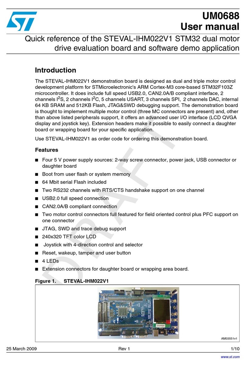
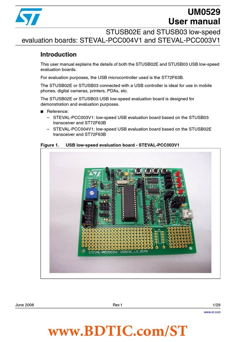
Figure 1. STEVAL-PLC001V1 evaluation board
UM2933
UM2933 - Rev 1 page 2/42

1Getting started
1.1 Safety precautions for use
The STEVAL-PLC001V1 evaluation board has a level of radiated emissions that exceeds the limit for class A
devices. Therefore, the user must add a proper shielding metal enclosure (Faraday cage) in the setup of the
evaluation environment of the board.
There are two peaks exceeding the limit to be observed for EU, FCC and ISED, the first at 324 MHz and the
second at 755.94 MHz, respectively exceeding for 11.6 dB µV/m and 1.0 dB µV/m.
Danger:
People with active implanted medical devices shall not use this evaluation kit, as safety related to
radiated emissions is not guaranteed.
1.2 Features
•STM32F746ZGT7 high-performance MCU embedding ARM® 32-bit Cortex®-M7 CPU with FPU, Chrom-ART
accelerator, and DSP instructions
•CLT01-38SQ7 octal high-speed digital input current limiter with SPI interface
•CLT03-2Q3 dual-channel self-powered digital input current limiter
•ISO8200AQ galvanic isolated octal high-side smart power solid-state relay with SPI interface
•IPS4260L quad low-side intelligent power switch
• Main supply voltage: 18 - 32 V (24 V nominal)
•STSW-PLC001 firmware package
• 3.5" TFT display with multitouch capability interfaced through dedicated parallel, digital RGB ports and I²C
lines
•STLD40DPUR-based display back-light LED driver with controllable intensity
• Morpho connectors for expansion connectivity options
• Screw connectors for safer power supply and industrial IO connections
• USB connector for alternate 5 V source power supply (only for display powering and MCU programming/
debug)
• Isolated USART port connector
• SWD connector for debugging and programming
• Status LEDs for inputs, outputs, and various fault conditions
• Debug LEDs
• Reset button
• Protections against surge, EMI, and input reverse voltage connection
• EMC pad and four-layer routing
• On-board RAM and serial Flash (ROM)
• Provision for RTC, USB (with one or more additional components to be mounted)
• Designed to meet IEC industrial standard requirements
• RoHS
1.3 Hardware architecture
The following block diagram shows the STEVAL-PLC001V1 architecture.
UM2933
Getting started
UM2933 - Rev 1 page 3/42

Figure 2. STEVAL-PLC001V1 functional block diagram
GPIO
opto
STM32F746ZG
Arm Cortex-M7 MCU with 1 Mbyte of
Flash memory, 216 MHz CPU
32.768kHz
xstal (RTC)
25 MHz
Oscill.
SDRAM
128Mb 166Mz
CLT03-2Q3
2-ch self-
powered
SWD connector
10-pin connector
USART connector
USB micro – AB
Demo mode
Morpho connector
2x38 strip male conn.
3.5 inches LCD
TouchGFX
ISO8200AQ
8-channel isolated HS
IPS4260L
4-channel LS
12 industrial output Screw connector
CLT03-38SQ7
8-channel high-speed
SPI
GPIO
opto
SPI
Isolator
GPIO
opto
SPI2
12 industrial input Screw connector
STL42P6LLF6
P-channel MOSFET
24 VDC
LDK220
200mA
LDO
5 V, 3.3 V
STLD40DPUR
Backlight LED driver
Current mode Step up
Converter
CLT03-2Q3
2-ch self-
powered
Protections + Filter
Various ICs
Non ST and
passive
components
LTDC (RGB)+
I2C
SPI
FLASH
1 MB
DC-DC
converter
Isolated
FMC
SPI
The main blocks are:
• the STM32F746ZGT7 microcontroller;
• twelve industrial inputs managed through the eight-channel CLT01-38SQ7 and the dual channel CLT03-2Q3
mounted twice;
• twelve industrial outputs on the bottom handled by other two dedicated ICs: the eight-channel ISO8200AQ
and the four-channel IPS4260L.
The architecture also includes a 3.5” TFT display powered by the TouchGFX graphics engine for great flexibility in
industrial IO management, giving abstraction from the hardware on one side, and full featured use of the ICs on
the other side.
The morpho connectors allow connecting expansion boards and the USB connector allows supplying the board in
case a 24 V power supply is not available.
Note: When powered through the USB port, the STEVAL-PLC001V1 has limited functionalities, as it works in demo
mode, allowing display management and programming features but not high current rates on the industrial IOs.
A screw connector in the bottom-left corner is provided to power the board. All other isolated and logic supply
voltages derive from this 24 V input after appropriate conditioning.
A P-channel MOSFET ensures reverse polarity protection, while other ICs are for EMI and surge protections.
A screw connector in the bottom-right corner powers field side devices.
UM2933
Hardware architecture
UM2933 - Rev 1 page 4/42

1.4 Board connections and components
Figure 3. STEVAL-PLC001V1 external connections
I0: 8 high side speed digital inputs
(CTL01-38SQ7 through SPI)
I0.0 I0.1 I0,2 I0.3 I0.4 I0.5 I0.6 I0.7
I1: 4 self-powered digital inputs
(high/low side via CTL03-2Q3)
24 V GND
0H
0L
1H
1L
2H
2L
3H
3L
24 V GND
Isolated serial connection
ST-LINK interface (for programming)
Optional 5 V input
(non-isolated, for demo mode only)
24 V input supply
Q0: 8 galvanic isolated high-side
digital outputs
(ISO8200AQ with SPI)
Q0.0 Q0.1 Q0.2 Q0.3 Q0.4 Q0.5 Q0.6 Q0.7
Q1: 4 low-side digital outputs
(IPS4260L)
Q1.0 Q1.1 Q1.2 Q1.3
24 V to field
-ve/+ve
UM2933
Board connections and components
UM2933 - Rev 1 page 5/42

Figure 4. STEVAL-PLC001V1 top components
1. CLT01-38SQ7 (U1) - high speed 8 digital inputs current limiter on SPI
2. CLT03-2Q3 (U4,U5) - self-powered digital input current limiter
3. EMIF08-LCD04M16 - 8-line L-C EMI filter and ESD protection for display interfaces
4. STL42P6LLF6 (Q4) - P-channel MOSFET (reverse voltage protection)
5. STLD40DPUR (U14) - white LED power supply for large display back-light
6. 40-pin FFC connector for LCD touch display (U15)
7. SM15T33CA (D39) - TVS diode
8. ISO8200AQ (U13) - galvanic isolated octal high side smart power solid state relay with SPI interface
9. IPS4260L (U8)- quad low-side intelligent power switch
12
3
456
789
UM2933
Board connections and components
UM2933 - Rev 1 page 6/42

Figure 5. STEVAL-PLC001V1 bottom components
1. Morpho connector
2. Morpho connector
3. STM32F746ZGT7 (U27) - high-performance and DSP with FPU Arm Cortex-M7 MCU
4. RAM
5. Flash memory
6. Isolation boundary
7. MCU reset switch (S2)
134
52
6
7
1.5 Main components
1.5.1 CLT01-38SQ7
The CLT01-38SQ7 is the 8-channel current limiter termination with high-speed SPI interface. The STEVAL-
PLC001V1 features daisy chain connection via SPI for this IC, the ISO8200AQ on the output side and the morpho
connectors. The three peripherals exploit daisy chain connection allowing less wiring on the PCB.
The CLT01-38SQ7 provides an 8-line protected digital input termination with serialized state transfer. It enhances
the I/O module density by cutting the dissipation (78 mW per input) and reducing the count of opto-transistors. Its
6.25 MHz SPI peripheral output serializes the input state transfer to the I/O module controller.
Available in a 7x7 QFN package with 48 leads, the device complies with the following standards: IEC61000-4-2
(±8 kV contact discharge and ±15 kV air discharge), IEC61000-4-4 (±4 kV) and IEC61000-4-5 (input = ±1 kV,
power supply = ±2.5 kV).
1.5.2 CLT03-2Q3
The CLT03-2Q3 is a digital input current limiter which drastically reduces the power dissipation of digital inputs. It
does not require external power supply as the device is activated with the input signal and consumes no power in
off state.
The CLT03-2Q3 features two independent channels and is high-side, low-side and reverse plug-in compatible. It
can drive opto-couplers or 3.3 V LVTTL circuits.
UM2933
Main components
UM2933 - Rev 1 page 7/42

The STEVAL-PLC001V1 hosts two CLT03-2Q3 in a 16-lead QFN package to reach a 12-input array. The device
enables industrial inputs to meet type 1 and 3 characteristic of IEC 61131-2 standard, while the IC complies with
the following standards:
• IEC 61000-4-2 level 1: ±4 kV (air discharge)
• IEC 61000-4-2 level 1: ±2 kV (contact discharge)
1.5.3 ISO8200AQ
The ISO8200AQ is a galvanic isolated 8-channel driver featuring a very low supply current. It embeds two
independent galvanic isolated voltage domains (VCC and VDD for process and control logic stages, respectively).
The IC is designed to drive any kind of load (inductive, resistive or capacitive) with one side connected to ground.
The control logic stage features an 8-bit output status register (where the microcontroller sets the ON/OFF status
of the output channels in the process stage) and an 8-bit fault register (where the OVT faults of each channel are
stored). The two stages communicate through the galvanic isolation channel via an ST proprietary protocol.
Active channel current limitation (OVL) combined with thermal shutdown (OVT), independent for each channel,
protects the device against overload and overtemperature. Additional embedded functions include loss of ground
protection, VCC and VDD UVLOs (with hysteresis), watchdog and VCC PGOOD.
An internal circuit provides an OR-wired not latched common (FAULT) indicator signaling the channel OVT. The
PGOOD diagnostic pin is activated if VCC falls below the power good internal threshold. Both FAULT and PGOOD
pins are open drain, active low, fault indication pins.
The device is UL1577 certified and is designed to meet IEC 61000-4-2, IEC 61000- 4-4, IEC 61000-4-5 and IEC
61000-4-8 standards. The package is TFQFPN32.
1.5.4 IPS4260L
The IPS4260L is a monolithic high speed (FSW up to 250 kHz) device, which can drive four independent
capacitive, resistive, or inductive loads with one side connected to the supply voltage. The channels can be
paralleled to reduce power dissipation.
When connected to VCC rail, four integrated catch diodes clamp the turn-off transients generated by inductive
loads even with huge inductance; combined with proper external TVS connected to VCC or to GND the IC allows
fast decay, too. Each channel is protected against overload or short-circuit: the intervention level can be set
by an external resistor on ILIM pin (see device data sheet for details). Built-in thermal shutdown protects the
chip against overtemperature even in case of short-circuit. If enabled, the integrated cut-off protection features a
non-dissipative protection in case of overload; it limits both the output average current value and, consequently,
the device overheating.
Cut-off delay/restart can be programmed by external resistors on CoD pin; it can be disabled by shorting CoD to
GND. Two common diagnostic open drains pins (OL, for open load and FLT for cut-off and thermal shutdown)
together with the four open drain on each INx pin (cut-off and thermal shutdown) feature an extensive diagnostic
of the chip.
The package is a miniaturized HTTSSOP20 and is designed to meet IEC 61131-2 standard.
1.5.5 STM32F746ZG
The STM32F746ZG microcontroller is the core of our evaluation board and is responsible for the management of
all industrial I/O ICs and for the HMI running on the 3.5 display with the TouchGFX technology.
The STM32F746xx devices are based on the high-performance ARM® Cortex®-M7 32-bit RISC core operating
at up to 216 MHz frequency. The Cortex®-M7 core features a single floating point unit (SFPU) precision which
supports all ARM® single-precision data-processing instructions and data types. It also implements a full set of
DSP instructions and a memory protection unit (MPU) which enhances the application security.
The STM32F746xx devices incorporate high-speed embedded memories with a Flash memory up to 1 Mbyte,
320 Kbytes of SRAM (including 64 Kbytes of Data TCM RAM for critical real-time data), 16 Kbytes of instruction
TCM RAM (for critical real-time routines), 4 Kbytes of backup SRAM available in the lowest power modes, and
an extensive range of enhanced I/Os and peripherals connected to two APB buses, two AHB buses, a 32-bit
multi-AHB bus matrix and a multi-layer AXI interconnect supporting internal and external memories access.
All the MCUs in this family offer three 12-bit ADCs, two DACs, a low-power RTC, thirteen general-purpose
16-bit timers including two PWM timers for motor control and one low-power timer available in stop mode, two
general-purpose 32-bit timers, a true random number generator (RNG). They also feature standard and advanced
communication interfaces. For further details, see the device data sheet.
UM2933
Main components
UM2933 - Rev 1 page 8/42
The LCD-TFT controller interface with dual-layer support takes advantage of the Chrom‑ART Accelerator. This
graphics accelerator creates content twice as fast as the core alone and features 2-D raw data copy, image format
conversion and image blending.
1.6 Digital inputs and outputs
The 12 digital inputs are arranged in groups of 8 and 4 channels. On the terminal block, they marked as I0 with 8
channels and provide 8 high side inputs to CLT01-38SQ7. Each channel is marked as I0.x (i.e. from I0.0 to I0.7).
Four high/low inputs for the two CLT03-2Q3 are accessible in the terminal block I1 (channels I1.0 to I1.3).
The 12 digital outputs are grouped similarly in two terminal blocks. 8 channels from IS08200AQ are marked Q0
on the terminal block, while 4 low side outputs from IPS4260L are in the terminal block Q1.
Input and output terminals are placed symmetrically.
1.7 Power distribution on the board
The STEVAL-PLC001V1 evaluation board is designed to work with 24 V nominal power supply. The MCU and
logic circuit are galvanically isolated from the field side circuit.
STL42P6LLF6 P-Channel MOSFET is crucial for the reverse polarity protection circuit ensuring low voltage drop
and high current capability in addition to quick response time. The board also provides suitable surge protection
and noise filtering.
Figure 6. Power and logic connections
ISO8200AQ
3.3 V
5 V
5V_CLT01
LDK220M3R
CLT01-
38SQ7
isolator
24 V
STL42P6LLF6
PMOS for
Reverse Voltage
Protection
DC-DC
converter
(24V to 5V)
STM32F746
MCU
IP4260L
16 V
STLD40DPUR
(backlight LED
driver)
RAM
3.5” LCD +
Touch
Screen
5 V
3.3 V
3.3 V
3.3 V
GPIO
SPI
LM7805
24 V
GPIO_OUT
SPI
opto
CLT03-2Q3
(self-powered)
CLT03-2Q3
(self-powered)
isolator
Field-side
device
Logic device
opto
FAULT_CH to MCU
USART_Tx
USART_Rx
MCU_Rx
MCU_Tx
FLASH
(demo mode)
USB MICRO-AB`
non-isolated
24 V
5V_field
5 V
3.3 V
16 V
Logic:
opto opto
SPI
5V_field
24 V
External logic
supply
24 V
5V Input
24 V
24 V
Field:
5V_CLT01 5V_field
opto
STLD40D is a boost converter (5 V supply to ~18 V) needed for the LCD back-light. The converter is a pulse
frequency modulation (PFM) inductor switch that can work in discontinuous mode (DCM). A minimum OFF time of
the embedded TSW boost switch is fixed internally and allows limiting the switching frequency. The output current
capability is 20 mA with an output voltage of 37 V (maximum rating). The regulation is done by sensing the LED
current through a current resistor (R86). The device can be turned ON/OFF through the logic enable signal pin
(EN). A low frequency PWM signal is used to dim the LCD back-light.
1.8 MCU interfaces and pin allocation
The SPI-2 interface is shared between CLT01-38SQ7 and ISO8200AQ with separate chip-select lines from the
MCU. CLT03-2Q3 and IPS4260L are interfaced through GPIO pins.
The ISO8200AQ and IPS4260L fault indications are interfaced with the MCU through dedicated GPIO inputs. Two
debug LEDs (D36, D39) are controlled through GPIO output.
The TFT display is connected through dedicated pins in RGB16 mode. i2C4 is used to interface the touch sensor
with the display. The touchscreen resolution is 800x480 while LCD screen resolution is 320x240. Thus, scaling is
applied to find the touch corresponding to the point on the LCD.
UM2933
Digital inputs and outputs
UM2933 - Rev 1 page 9/42

Morpho connectors (J17, J18) gives provision for connectivity with compatible boards such as STEVAL-
IOM001V1 if you want to add IO-Link master capabilities to our PLC.
For further details on MCU interfaces, see Section Appendix A which summarizes the information contained in
the .ioc file provided with the STSW-PLC001 firmware and the schematic.
1.9 External memory interface
Serial Flash (U20) interfaces with the MCU via SPI5. The size of the serial flash is 1 Mbits. The address for
read/write is in the range of 0x000000 to 0x01FFFF. Sample read/write routines are provided in the firmware.
The FMC controller inside STM32 accesses the SDRAM (U19). In this application, 12 bit addressing is used along
with 16-bit data line. The HADDR[28] bit is used to select one of the two memory banks in the example code.
However, the memory can be used in 8-bit, 16-bit or 32-bit mode.
1.10 Jumper selection, LED indicators and test points
The recommended jumper settings for default option in the firmware are:
• for module I0: J2 – Pin 1, 2 short (MISO); J4 pin 3-2 short (8-bit mode)
• for module Q1: J10, J12 closed and J8 and J9 open
Table 1. LED indicators
Type Name Description
Power indication D40 Board input power indicator.
Power Good and Fault D29, D34 Fault indication for ISO8200AQ IC.
Fault and Overload D21, D22 Fault Indication for IPS4260L.
Debug D36 (amber), D37 (blue) To indicate program heartbeat, fault condition, etc. as per use case.
Input status D1-D8
D9-D12 Status of digital inputs.
Output status D24-D33
D13-D16 Status of digital outputs.
Note: D22 is triggered by the OL pin of IPS4260L, which indicates open load condition or short to ground condition.
Open load detection feature is activated by placing proper resistors between LOADx and PGND ground plane.
In the STEVAL-PLC001V1 evaluation board, there are resistors placed for open load detection for the Q1.X four
outputs. For Q1.2 and Q1.3, instead, they are activated only if J8 and J9 jumpers are closed. Thus, the Fault
LED (D22) might glow when there is no load connection or partial connection to output terminals.
Numerous test points are provided on the board (see Section 4 Schematic diagrams).
UM2933
External memory interface
UM2933 - Rev 1 page 10/42

2How to run the evaluation board with the preloaded firmware
To run the STEVAL-PLC001V1 evaluation board with the STSW-PLC001 preloaded firmware, you have two
possibilities to power the board up:
1. through the micro-USB connector with an appropriated power supply (i.e. 5 V, 1 A): with this option, you
can access limited board functions like programming/debugging through the SWD connector or use the
touchscreen display to show the features of the industrial ICs mounted on the board. This mode is intended
for demonstration only or to use MCU logic circuit only;
2. through the screw connector (24 V) placed in the bottom-left corner: this option offers the complete
experience with the STEVAL-PLC001V1, that is all programming/debugging and display features can be
executed, and the industrial I/O can be handled with the highest possible current ratings allowed by the
ICs (i.e. you can drive several output loads requiring up to 0.7 A of current each through the output screw
connector placed on the bottom side).
STSW-PLC001 provides the framework to use all the STEVAL-PLC001V1 modules including TouchGFX-based
HMI. After powering up, you just have to select one of the user modes through the touchscreen.
UM2933
How to run the evaluation board with the preloaded firmware
UM2933 - Rev 1 page 11/42

3Firmware overview and architecture
The STSW-PLC001 companion software package is available for download at www.st.com. It is designed as a
development tool for industrial PLCs.
To use the STEVAL-PLC001V1 board and the associated firmware, power supply the board (24 V or through a
portable USB power supply) and play with the user interface powered by the TouchGFX technology featuring HMI
capabilities. Freely customizable C-code written examples are also provided to speed up the development time.
Figure 7. STSW-PLC001 block diagram
User input & display
User APIs, predefined
use cases
User application & demo
timers & utility functions
Board support routines
TouchGFX engine
FreeRTOS
HAL component
STM32 HAL Library
For further details on user APIs, touch display engine and demonstration use-cases, refer to the STSW-PLC001
user manual (UM2938, freely available on www.st.com).
UM2933
Firmware overview and architecture
UM2933 - Rev 1 page 12/42

4Schematic diagrams
Figure 8. STEVAL-PLC001V1 circuit schematic (1 of 9)
STM32F746
SPI2_NSS
SPI2_SCK
SPI2_MISO
SDO_DAISY
PD6/B2
SPI2_ISO_MOSI
SPI2_MORPHO_MOSI
LCD_CLK
LCD_HSYNC
LCD_SDA
LCD_DE
LCD_INT
VDD
ENCQ
IO-RST
L+ON
IRQ
ENL+
I2C1_SCL
UART4_TX
UART4_RX
OL-OFF
SPI5_NSS
SPI5_WP
SPI5_HOLD
SPI5_MOSI
SPI5_SCK
I2C1_SDA
UART5_RX
GND_Logic
BLUE[0..5]
RED[0..5]
LCD_VSYNC
LCD_SCL
DATA[0..15]
ADD[0..13]
FMC_CTRL[0..7]
SPI5_MISO
USB[0..5]
PA1
DI_FLT_Q1_3
3V3
DI_FLT_Q1_FLT
DI_FLT_Q1_4
DI_FLT_Q1_OL
DI_FLT_Q1_2
DI_FLT_Q1_1
DO_Q1_1
DO_Q1_2
DO_Q1_3
DO_Q1_4
DI_I1_1
DI_I1_2
DI_I1_3
DI_I1_4
DO_LCD_BL_CTRL
DI_Q0_PGOOD
DI_Q0_FLT
DO_Q0_EN
GREEN[0..5]
BOOTO
LCD_DISP
LCD_RESET
MCU_RST
ISO8200AQ
SPI2_NSS
SDO_DAISY
SPI2_MISO
SPI2_SCK
SPI2_MORPHO_ISO
VDD
24V_Field
SPI2_MORPHO_MOSI
GND_Field
GND_Logic
DI_Q0_PGOOD
DI_Q0_FLT
DO_Q0_EN
Q0.1
Q0.2
Q0.3
Q0.4
Q0.5
Q0.6
Q0.7
Q0.0
LCD
LCD_DE
LCD_HSYNC
LCD_INT
LCD_CLK
LCD_SDA
5V
VDD
GND_Logic
BLUE[0..5]
RED[0..5]
LCD_VSYNC
LCD_SCL
DO_LCD_BL_CTRL
GREEN[0..5]
LCD_DISP
LCD_RESET
CLT01-38SQ7
SPI2_MISO
SDO_DAISY
SPI2_SCK
SPI2_NSS
PD6/B2
GND_Field
GND_Logic
24V_Field
VDD
I0.1
I0.2
I0.3
I0.4
I0.5
I0.6
I0.7
I0.0
Power
5V
24V_Field
VDD
5V_Field
24V
GND_Field
GND_Logic
GND_IN
USB[0..5]
3V3
IPS4260L
24V_Field
GND_Field
5V_Field
DI_FLT_Q1_3
DI_FLT_Q1_FLT
DI_FLT_Q1_4
DI_FLT_Q1_OL
DI_FLT_Q1_2
DI_FLT_Q1_1
DO_Q1_1
DO_Q1_2
DO_Q1_3
DO_Q1_4
VDD
GND_Logic
Q1.0
Q1.3
Q1.2
Q1.1
Morpho & Memory
ENCQ
UART4_TX
UART4_RX
IO-RST
L+ON
IRQ
UART5_RX
I2C1_SCL
I2C1_SDA
SPI2_SCK
SPI2_MORPHO_ISO
SPI2_MISO
SPI2_NSS
ENL+
OL-OFF
SPI5_NSS
SPI5_WP
SPI5_HOLD
SPI5_SCK
SPI5_MOSI
SPI5_MISO
SPI2_ISO_MOSI
VDD
GND_Logic
DATA[0..15]
ADD[0..13]
FMC_CTRL[0..7]
PA1
MCU_RST
CLT03-2Q3
24V_Field
VDD
GND_Field
GND_Logic
DI_I1_1
DI_I1_2
DI_I1_3
DI_I1_4
I1.0L
I1.2L
I1.1L
I1.0H
I1.2H
I1.3H
I1.1H
I1.3L
24V_Field
VDD
5V
GND_Logic
VDD
5V
GND_Logic
5V_Field
24V_Field
GND_Field
DI_FLT_Q1_3
DO_Q1_4
DO_Q1_3
DO_Q1_2
DO_Q1_1
SPI2_ISO_MOSI
ENL+
OL-OFF
I2C1_SDA
I2C1_SCL
UART5_RX
IO-RST
UART4-TX
UART4-RX
ENCQ
SPI5_WP
SPI5_NSS
SPI5_HOLD
SPI5_SCK
SPI5_MOSI
GND_Field
GND_Logic
VDD
GND_Field
VDD
GND_Logic
24V_Field
SDO_DAISY
SPI2_SCK
SPI2_NSS
SPI2_MISO
DI_FLT_Q1_OL
DI_FLT_Q1_FLT
DI_FLT_Q1_1
DI_FLT_Q1_2
DO_Q0_EN
DI_Q0_PGOOD
DI_Q0_FLT
VDD
GND_Logic
24V_Field
GND_Field
VDD
GND_Logic
VDD
GND_Logic
24V_Field
GND_Field
5V_Field
L+ON
IRQ
SPI5_MISO
LCD_RED[0..5]
LCD_BLUE[0..5]
LCD_DE
LCD_CLK
LCD_SDA
LCD_INT
LCD_HSYNC
LCD_VSYNC
LCD_SCL
LCD_RST
DO_LCD_BL_CTRL
USB[0..5]
FMC_ADD[0..13]
SPI2_MISO
PD6/B2
SPI2_NSS
SPI2_SCK
SDO_DAISY
FMC_DATA[0..15]
FMC_CTRL[0..7]
DI_I1_1
DI_I1_2
DI_I1_3
DI_I1_4
SPI2_SCK
SPI2_NSS
SPI2_MISO
PA1
DI_FLT_Q1_4
3V3
3V3
LCD_GREEN[0..5]
MCU_RST
BOOTO
LCD_DISP
SPI2_MORPHO_ISO
SPI2_MORPHO_ISO
MCU_RST
UM2933 - Rev 1 page 13/42
UM2933
Schematic diagrams

Figure 9. STEVAL-PLC001V1 circuit schematic (2 of 9)
Data out= /MISO
INPUT
Data out= MISO
GND_CLT1
16 bits
Isolation Barrier
CLT01-38SQ7
MO-A2
I0.0
I0.1
I0.2
I0.3
I0.4
I0.5
I0.6
I0.7
24V_Field
VDD
SDO_DAISY
SPI2_SCK
SPI2_NSS
PD6/B2
SPI2_MISO
GND_Logic
GND_Field
VDD_CLT
VDD_CLT
VDD_CLT VDD
VDD
U1
CLT01_38SQ7_TR
VDD
1
DVR
2
NC_1
3
SPM
4
NC_2
5
NC_3
6
COMP_1
7
NC_4
8
NC_5
9
NC_6
10
NC_7
11
NC_8
12
13
VC
14
VCS
15
COMP_2
16
IN1
17
IN2
18
IN3
19
IN4
20
COMP_3
21
IN5
22
IN6
23
IN7
24
IN8
25
NC_9
26
NC_10
27
NC_11
28
NC_12
29
NC_13
30
NC_14
31
COMP_4
32
NC_15
33
NC_16
34
LED8
35
LED7
36
LED6
LED5 37
LED4 38
LED3 39
LED2 40
LED1 41
REF 42
COMS 43
MISO_MISO 44
NC_17 45
MOSI 46
SCK 47
_CS 48
49
D4
GREEN
A C
C7
22nF
D8
GREEN
A C
R5
15K
R16
120K
C10
22nF
R20 120E
R81K
U2
SI8661BD-B-IS
VDD1
1
A1
2
A2
3
A3
4
A4
5
A5
6
A6
7
GND1
8GND2 9
B6 10
B5 11
B4 12
B3 13
B2 14
B1 15
VDD2 16
R13
D5
GREEN
A C
D1
GREEN
A C
C12
22nF
C8
22nF
C14
100nF
R60E
R22 2K2
C129
DNM
C15
10uF
J1
CON8
1
2
3
4
5
6
7
8
R10
1K
D2
GREEN
A C
C16
100nF
C3 33pF
C18
22nF
R17 2K2
R7 2K2
D6
GREEN
A C
TP1
NM
1
C9
22nF
TP2
NM
1
R19 2K2
D3
GREEN
A C
TP3
NM
1
J4
3 pin jumper
1
2
3
R21
R15 1M5
C5
4.7uF
TP4
NM
1
R9 2K2
TP14
NM
1
R1940.0
D7
GREEN
A C
R18 120E
NM
C6
100nF
R12 2K2
J2
3 pin jumper
1
2
3
CLT_CS1
CLT_SCK
CLT_MOSI
CLT_MISO
I0 .0
CLT_IN1
I0 .0
I0 .1 I0 .1
CLT_IN2
I0 .2
I0 .3
I0 .4
I0 .5
I0 .6
I0 .7 I0 .2
CLT_IN3
I0 .3
CLT_IN4
CLT_IN1
CLT_IN2
CLT_IN3
CLT_IN4
CLT_IN5
CLT_IN6
CLT_IN7
CLT_IN8
I0 .4
CLT_IN5
I0 .5
CLT_IN6
CLT_MOSI
CLT_SCK I0 .6
CLT_IN7
CLT_CS1
CLT_MISO
I0 .7
CLT_IN8
GND_Field
GND_Logic
GND_Field
GND_Field
GND_Field
GND_CLT1
HIGH SIDE DIGITAL INPUTS
8 bits
GND_Logic
GND_CLT1
GND_CLT1
GND_Field
GND_Field
GND_CLT1
GND_CLT1 GND_Field
GND_Field
I0.0
I0.1
I0.2
I0.3
I0.4
I0.5
I0.6
I0.7
C4 33pF
C2 33pF
R8 1K
1K
R11 2K2
C1 33pF
C11
33nF
J1
CON8
1
2
3
4
5
6
7
8
R1
220R
R2
C17
22nF
1
NM
1
R3
1
J4
1
2
3
120E
1
1
R194 0.0
C13
22nF
1
2
3
R14 2K2
I0 .0
I0 .1
I0 .2
I0 .3
I0 .4
I0 .5
I0 .6
I0 .7
220R220R220R
R4
UM2933 - Rev 1 page 14/42
UM2933
Schematic diagrams

Figure 10. STEVAL-PLC001V1 circuit schematic (3 of 9)
CLT03-2Q3
Isolation Barrier
VDD
24V_Field
GND_Logic
GND_Field
DI_I1_1
DI_I1_2
R23, R24, R25, R26
Can be replaced by a capacitor for test purpose
DI_I1_3
DI_I1_4
I1.3L
I1.2H
I1.2L
I1.0L
I1.0H
I1.1H
I1.1L
I1.3H
VDD
VDD
C22
4.7uF
1
PD2
U4 CLT03-2Q3
3
INA2
2INATTL2
4
INB2
5
OUTN1
6
INATTL1
7
INA1
8
INB1
TP1
9
VBUF1
10
OUTP1
11
PD1
OUTN2
13
TP2
14
VBUF2
15
16
OUTP2
OUTN1_T
TAB1
OUTN2_T
TAB2
C20
10nF
C26
10nF 0
R199
C28
10nF
C25 10nF
D52 3.3V NM
A C
D12 GREEN
TP5
NM
1
0
R200
C23
10nF
R26 0E
D53 3.3V NM
C29
100nF
U5
1
PD2
CLT03-2Q3
3
INA2
2INATTL2
4
INB2
5
OUTN1
6
INATTL1
7
INA1
8
INB1
9
TP1
10
VBUF1
OUTP1
11
PD1
12
13
OUTN2
TP2
14
VBUF2
15
OUTP2
16
OUTN1_T
TAB1
OUTN2_T
TAB2
C24
100nF
R201 7.5K
TP6
NM
1
D50 3.3V NM
J7
1
2
CON6-2315
3
4
5
6
C21 10nF
R204 7.5K
U6
1
ACPL-024L-000E
ANODE1
2CATHODE1
3CATHODE2
4ANODE2 GND 5
V02 6
V01 7
VDD 8
C27 10nF
R203 7.5K
C19 10nF
R202 7.5K
U3
1ANODE1
ACPL-024L-000E
2CATHODE1
3CATHODE2
4ANODE2 GND 5
V02 6
V01 7
8
VDD
0
R197
R24 0E
D51 3.3V NM
R25 0E
J6
1
2
CON6-2315
3
4
5
6
C30
4.7uF
R23 0E
0
R198
A C
D10 GREEN
A C
D11 GREEN
A
D9 GREEN
C
OUTP2
OUTN1
OUTN2
OUTN3
OUTN4
VDD
I1.2H
I1.2L
OUTN4
OUTP3
OUTP4
I1.3H
I1.0H
OUTP1
OUTN1
I1.0L
I1.1H
OUTP2
OUTN2
I1.1L
I1.0H
I1.0L
I1.1H
I1.1L
I1.2H
I1.2L
I1.3L
OUTP3
OUTP1
OUTN3
I1.3L
I1.3H
OUTP4
I1.0H
I1.1H
I1.2H
I1.3H I1.3L
I1.0L
I1.1L
I1.2L
INPUT
HIGH/LOW DIGITAL INPUTS
GND_Logic
GND_Field
GND_Logic
Either High (I1.xH) or Low (I1.xL) side in-out can be selected.
Corresponding Low or High terminal to be connected accordingly.
3.3V
A C
D12GREEN
TP5
NM
1
D53 3.3V NM
3.3V
C19 10nF
C
OUTP2
OUTN1
OUTN2
OUTP1
UM2933 - Rev 1 page 15/42
UM2933
Schematic diagrams

Figure 11. STEVAL-PLC001V1 circuit schematic (4 of 9)
Isolation Barrier
MO- A1
MO- B3
MO- A2
Q0.1
Q0.2
Q0.3
Q0.4
Q0.5
Q0.6
Q0.7
Q0.0
SPI2_NSS
SPI2_MISO
SPI2_MORPHO_MOSI
SPI2_SCK
SPI2_MORPHO_ISO
VDD
24V_Field
SDO_DAISY
GND_Logic
GND_Field
DO_Q0_EN
DI_Q0_PGOOD
DI_Q0_FLT
VDD
VDD
VDD
VDD
VDD
R82 220E
R69 220E
C50
10pF
C53
33pF
C47 22nF
C54
33pF
D33 GREEN
A C
C58 22nF
R76
750E
D28 GREEN
A C
TP10
NM
1
R80 7.5K
C52 22nF
C60
4.7uF
R72 NM
NM
J14
CON8
1
2
3
4
5
6
7
8
C61
100nF
C55
33pF
R77 7.5K
R81
750E
C51 22nF
C46
10pF
D25 GREEN
A C
R68 220E
C49 22nF
D29
RED
AC
R70 7.5K
U13
ISO8200AQ
GND_DD
1
GND_CC_1
3
OUT8_2
4
OUT8_1
5
OUT7_2
6
OUT7_1
7
OUT6_1
9
OUT6_2
8
OUT5_1
11
OUT5_2
10
OUT4_1
13
OUT4_2
12
OUT3_1
15
OUT3_2
14
OUT2_1
17
OUT2_2
16
OUT1_1
19
OUT1_2
18
VDD
20
OUT_EN
21
SS
22
CLK
23
SDI
24
PGOOD
25
SDO
31
FAULT
32
GND_CC_2
TAB1
GND_CC_3
TAB2
GND_CC_4
TAB3
VCC
TAB4
D31 GREEN
A C
D32 GREEN
A C
R64
1K
C56 22nF
D27
ESDALC6V1-1M2
TP9
NM
1
R79 7.5K
R65
10K
R66 7.5k
R78 220E
R71 220E
D34
GREEN
AC
R75 100E
NM
+
C45
4.7uF/63V
12
SW1
1437566-3
D24 GREEN
A C
R63 7.5K
D26 GREEN
A C
R74 220E
R73 7.5K
R67 7.5K
C59 22nF
C57
33pF
C48 22nF
D30 GREEN
A C
PGOOD
Q0.7
Q0.6
Q0.5
Q0.4
Q0.2
Q0.1
Q0.0
Q0.3
PGOOD
Q0.7
Q0.6
Q0.5
Q0.4
Q0.3
Q0.2
Q0.1
Q0.0
VDD
GND_Field
Q0.0
Q0.1
Q0.3
Q0.6
Q0.4
Q0.2
Q0.7
Q0.5
GND_Logic
GND_Logic GND_Field
GND_Field
PLC Digital output 1-8 (high side)
ISO8200AQ
UM2933 - Rev 1 page 16/42
UM2933
Schematic diagrams

Figure 12. STEVAL-PLC001V1 circuit schematic (5 of 9)
IPS4260L
PLC DIGITAL OUTPUT 9-12 (LOW-SIDE)
Isolation Barrier
IPS4260L
GND_Field
GND_Field
GND_Logi c
GND_Logi c
GND_Logi c
GND_Logi c
GND_Logi c
GND_Logi c
GND_Logi c
GND_Logi c
GND_Signal
GND_Signal
GND_Signal
GND_Signal
GND_Signal
GND_Signal
GND_Signal
GND_Signal
GND_Signal
.
To Field Side devices
DO_Q1_4
DO_Q1_3
DO_Q1_2
DO_Q1_1
DI_FLT_Q1_4
DI_FLT_Q1_3
Q1.3
Q1.2
Q1.1
Q1.0
5V_Field
GND_Field
24V_Field
DI_FLT_Q1_2
DI_FLT_Q1_1
DI_FLT_Q1_OL
DI_FLT_Q1_FLT
VDD
GND_Logic
24V_Field
VDD
VDD
VDD
R51
2.5K
R46 510R
R195
0.0
R47
60.4K
R27
7.5K
R34 330R
R52
1K
C32
1pF
C34
1uF
C38
1pF
C40
1uF
J9
2 pin jumper 2.54mm
J13
CON2
1
2
R45
52K
D22
RED
AC
C39
1pF
U11
ACPL-024L-000E
ANODE1 1
CATHODE1 2
CATHODE2 3
ANODE2 4
GND
5
V02
6
V01
7
VDD
8
R53 200R
J11
CON2
1
2
D15
GREEN
AC
R57 200R
D20 BAT20JFILM
R58 620R
U9
ACPL-024L-000E
ANODE1
1
CATHODE1
2
CATHODE2
3
ANODE2
4GND 5
V02 6
V01 7
VDD 8
+
C37
4.7uF/63V
12
D13
GREEN
AC
U10
ACPL-024L-000E
ANODE1 1
CATHODE1 2
CATHODE2 3
ANODE2 4
GND
5
V02
6
V01
7
VDD
8
C35
100nF
R30
7.5K
U8
IPS4260L
VZ1
3PGND2
2PGND1
1
SGND
8
IN3
6
IN4
7
IN1
4
IN2
5
OL
9
FLT
10
EP
21
PGND4 20
LOAD4
14
VZ2 18
LOAD3 15
PGND3 19
VCC 13
LOAD1 17
LOAD2 16
ILIM 12
CoD 11
R59 620R
R50 200R
J10
2 pin jumper 2.54mm
D23
SMC30J22CA
R60 200R
D21
RED
AC
R41 5.1K
R35 5.1K
C44
100nF
D17 BAT20JFILM
R44
220K
R54 620R
R40
52K
R48 510R
J8
2 pin jumper 2.54mm
R62 620R
R28
7.5K
C42
100nF
R56 200R
TP7
1
R61 200R
R33 5.1K
R55 620R
J26
CON2
1
2
R32 510R
D19 BAT20JFILM
C43
1uF
C41
100nF
C130
1nF
C31
100nF
U7
ACPL-024L-000E
ANODE1
1
CATHODE1
2
CATHODE2
3
ANODE2
4GND 5
V02 6
V01 7
VDD 8
R39 330R
U12
ACPL-024L-000E
ANODE1 1
CATHODE1 2
CATHODE2 3
ANODE2 4
GND
5
V02
6
V01
7
VDD
8
TP8
1
R29
7.5K
R43 5.1K
D18 BAT20JFILM
R36 510R
R37
52K
C33
1pF
D16
GREEN
AC
R38
52K
C36
100n
J12
2 pin jumper 2.54mm
R49 620R
D14
GREEN
AC
R31 330R
C95
10uF
R42 330R
VZ2
5V_Field
IN4_FLT
5V_Field OL
IN1_FLT
IN2_FLT
IN3_FLT
24V_Field
24V_Field
VZ1
FLT
OL
IN1_FLT
IN2_FLT
5V_Field
5V_Field
IN3_FLT
IN4_FLT
FLT
FLT
OL
Q1.3
Q1.1
Q1.2
VZ1
5V_Field
Q1.3
Q1.2
Q1.0
Q1.1
VZ2
Q1.0
24V_Field
GND_Field
GND_Signal GND_Field
PULL DOWN
RESISTORS
FOR OPEN LOAD
DETECTION
IN OFF STATE
Default both J10 and J12 closed
UM2933 - Rev 1 page 17/42
UM2933
Schematic diagrams

Figure 13. STEVAL-PLC001V1 circuit schematic (6 of 9)
STM32F746ZGTx
Optional
Programming Pins
For making isolated serial
connection, connect Pin1
and 2 of J22 and J23.
For Using IO Board e.g
P-NUCLEO-IOM01M1 through
Morpho, connect Pin3 and 2
of J22 and J23.
GND_Logic
GND_Logic
GND_Logi c
GND_Logic
GND_Logi c
GND_Logi c
GND_Logic
GND_Logic
GND_Logic
GND_Logic
GND_Logic
GND_Logic
GND_Logic
GND_Logic
GND_Logic
GND_Logic
GND_Logic
To be mounted to enable real-time clock
MO- A1
MO- A2
MO- A3
SPI2_NSS
SPI2_SCK
SPI2_MISO
SDO_DAISY
PD6/B2
SPI2_ISO_MOSI
LCD_CLK
LCD_HSYNC
LCD_SDA
LCD_INT
ENCQ
IO-RST
IRQ
ENL+
I2C1_SCL
UART4_TX
UART4_RX
BOOTO
OL-OFF
SPI5_NSS
SPI5_WP
SPI5_MOSI
SPI5_SCK
I2C1_SDA
UART5_RX
SPI2_MORPHO_MOSI
DO_Q1_1
DO_Q1_2
DO_Q1_3
DO_Q1_4
DI_FLT_Q1_4
GND_Logic
DI_I1_1
DI_I1_2
DI_I1_3
DI_I1_4
VDD
LCD_DE
BLUE[0..5]
RED[0..5]
L+ON
DO_Q0_EN
DI_FLT_Q1_OL
DI_FLT_Q1_2
DI_FLT_Q1_1
DI_FLT_Q1_FLT
DI_Q0_PGOOD
DI_Q0_FLT
DATA[0..15]
LCD_VSYNC
MCU_RST
LCD_SCL
ADD[0..13]
FMC_CTRL[0..7]
SPI5_MISO
SPI5_HOLD
USB[0..5]
GREEN[0..5]
PA1
3V3
LCD_DISPDI_FLT_Q1_3
DO_LCD_BL_CTRL
MCU_RST LCD_RESET
VDD
VDD
VDD
VDD
VDD
VDD
VDD
VDD
VDD
VDD
VDD
VDD
VDD
J25
con5-strip-male
1
2
3
4
5
R167 2K7
STM32F746ZGT7
U27B
VBAT
6
VDDUSB
95
VSS
16
VSS_2
51
VSS_8
130
VSS_4
83
VSS_1
38
VSS_3
61
VSS_5
94
VSS_6
107
VSS_7
120
VSSA
31
VDDA
33
VDD_2 39
VDD_5 72
VDD_3 52
VDD_6 84
VDD_8 121
VDD_4 62
VDD_7 108
VDD_9 131
VDD 17
VDD_10 144
VDD_1 30
VCAP_1 71
VCAP_2 106
VREF+ 32
C109
100nF
Y1
NX3215SA-32.768K
D49
ESDALC6V1-1M2
R181
10K
NM
R159 0
NM
C111
1uF
BT1
3030TR
NM
+1 1
+2 2
-
3
SW2
1437566-3
0 0
L6
600 Ohms
1 2
R162 0
C116
100nF
C124
4.7pF_NPO_-+0.25pF_0402
R157 0E
C121
100nF
U27A
STM32F746ZGT7
PE0
141
PE1
142
PE2
1
PE3
2
PE4
3
PE5
4
PE6
5
PE7
58
PE8
59
PE9
60
PE10
63
PE11
64
PE12
65
PE13
66
PE14
67
PE15
68
PF0
10
PF1
11
PF2
12
PF3
13
PF4
14
PF5
15
PF6
18
PF7
19
PF8
20
PF9
21
PF10
22
PF11
49
PF12
50
PF13
53
PF14
54
PF15
55
PG0 56
PG1 57
PG2 87
PG3 88
PG4 89
PG5 90
PG6 91
PG7 92
PG8 93
PG9 124
PG10 125
PG11 126
PG12 127
PG13 128
PG14 129
PG15 132
PH0 23
PH1 24
NRST 25
BOOT0 138
PDR_ON 143
R163 0E NM
C112
100nF
R175
200
R160 0E
R1910
C114
100nF
R174
200
R182
10K
C101
2.2uF (Low ESR)
C122
100nF
R164 0
C108
100nF
C104
1uF
C125
4.7pF_NPO_-+0.25pF_0402
R184
0
NM
R180 0
R161 0E
NM
R165
100
R177
100
C123
100nF
C105
100nF
R171
10K
C107
100nF
R168
0
C120
100nF
J24
3 pin jumper
1
2
3
C117
100nF
TP15
1
R172 50
R179
10K
C102
2.2uF (Low ESR)
R153 0E
C119
100nF
R206
0
NM
R155 120
+
C110
220uF
NM
12
C100
100nF
C127
100nF
R183 10k
R152 0ENM
R178 100_1%
J23
CON10A
1 2
3 4
5 6
7 8
9 10
R156 0
R176
100
J22
3 pin jumper
1
2
3
R154 0
NM
R158 0
R185 0
R205
0
U28
ILD207T
A1
1
K1
2
A2
3
K2
4E2 5
C2 6
E1 7
C1 8
Y2
ECS-2520MV-250-BN-TR
2
4 3
1
R170
10K
NM
R169 2K7
C113
100nF
C126
100nF
R173 0
STM32F746ZGT7
U27C
PA0
34
PA1
35
PA2
36
PA3
37
PA4
40
PA5
41
PA6
42
PA7
43
PA8
100
PA9
101
PA10
102
PA11
103
PA12
104
PA13
105
PA14
109
PA15
110
PB0
46
PB1
47
PB2
48
PB3
133
PB4
134
PB5
135
PB6
136
PB7
137
PB8
139
PB9
140
PB10
69
PB11
70
PB12
73
PB13
74
PB14
75
PB15
76
PC0 26
PC1 27
PC2 28
PC3 29
PC4 44
PC5 45
PC6 96
PC7 97
PC8 98
PC9 99
PC10 111
PC11 112
PC12 113
PC13 7
PC14 8
PC15 9
PD0 114
PD1 115
PD2 116
PD3 117
PD4 118
PD5 119
PD6 122
PD7 123
PD8 77
PD9 78
PD10 79
PD11 80
PD12 81
PD13 82
PD14 85
PD15 86
C103
100nF
C118
100nF
C106
100nF
C115
100nF
RCC_OSC32_OUT
RCC_OSC32_IN
FMC_ADD.A0
FMC_ADD.A1
FMC_ADD.A2
FMC_ADD.A3
FMC_ADD.A4
FMC_ADD.A5
RCC_OSC_IN
LCD_RST
RED.R5
FMC_CTRL.SDCKE0
BLUE.B5
GREEN.G2
RED.R4
FMC_CTRL.SDNE0
RED.R6
RED.R3
FMC_CTRL.SDNRAS
FMC_ADD.A6
FMC_ADD.A7
FMC_ADD.A8
FMC_ADD.A9
FMC_ADD.A10
FMC_ADD.A11
FMC_DATA.D4
FMC_DATA.D5
FMC_DATA.D6
FMC_DATA.D7
FMC_DATA.D8
FMC_DATA.D9
FMC_DATA.D10
FMC_DATA.D11
FMC_DATA.D12
GREEN.G5
GREEN.G4
LCD_SDA
FMC_DATA.D14
FMC_DATA.D15
FMC_DATA.D0
FMC_DATA.D1
FMC_ADD.BA_0
FMC_ADD.BA_1
RED.R7
FMC_CTRL.SDCLK
GREEN.G6
SYS_JTCLK-SW CLK
FMC_DATA.D2
FMC_DATA.D3
GREEN.G7
BLUE.B4
BLUE.B3
GREEN.G3
SYS_JTDO-SW O
SYS_JTRST
BLUE.B7
BLUE.B6
FMC_CTRL.NBL1
PDR_ON
RED.R2
RED.R3
RED.R4
RED.R5
RED.R6
RED.R7
USART3_TX VDD_EXT
TX_EXT
GND_EXT
USART3_RX
GND_EXT
RCC_OSC32_IN
RCC_OSC32_OUT
RCC_OSC_IN
BOOT0
PDR_ON
SYS_JTMS-SW DIO
SYS_JTCLK-SW CLK
SYS_JTDO-SW O
SYS_JTDI
MCU_RST
USB.POW ER_SWITCH_ON
USB.OVER_CURRENT
RX_EXT
FMC_CTRL.SDNW E
SYS_JTDI
SYS_JTMS-SW DIO
USB.OTG_FS_DP
USART3_TX
USART3_RX
PC10
PC10
PC11
PC11
FMC_CTRL.NBL0
VDD
MCU_RST
BLUE.B2
BLUE.B3
BLUE.B4
BLUE.B5
BLUE.B6
LCD_BLUE[0..5]
LCD_BLUE[0..5]
BLUE.B7
FMC_DATA.D13
LCD_RED[0..5]
LCD_RED[0..5]
VDD_EXT
TX_EXT
GND_EXT
GND_EXT
RX_EXT FMC_DATA.D14
FMC_DATA.D15
FMC_DATA.D13
FMC_DATA.D12
FMC_DATA.D11
FMC_DATA.D10
FMC_DATA.D9
FMC_DATA.D8
FMC_DATA.D7
FMC_DATA.D6
FMC_DATA.D5
FMC_DATA.D4
FMC_DATA.D3
FMC_DATA.D2
FMC_DATA.D1
FMC_DATA.D0 FMC_DATA[0..15]
FMC_DATA[0..15]
FMC_ADD[0..13]
FMC_ADD.BA_0
FMC_ADD.BA_1 FMC_ADD[0..13]
FMC_ADD.A0
FMC_ADD.A1
FMC_ADD.A2
FMC_ADD.A3
FMC_ADD.A4
FMC_ADD.A5
FMC_ADD.A6
FMC_ADD.A7
FMC_ADD.A8
FMC_ADD.A9
FMC_ADD.A10
FMC_ADD.A11
FMC_CTRL[0..7]
FMC_CTRL.NBL0 FMC_CTRL[0..7]
FMC_CTRL.NBL1
FMC_CTRL.SDCLK
FMC_CTRL.SDCKE0
FMC_CTRL.SDNE0
FMC_CTRL.SDNRAS
FMC_CTRL.SDNCAS
FMC_CTRL.SDNW E
FMC_CTRL.SDNCAS
USB.OTG_FS_DM
RED.R2
USB.OTG_FS_ID
USB.OTG_FS_VBUS
USB[0..5]
USB.POW ER_SWITCH_ON
USB[0..5]
USB.OVER_CURRENT
USB.OTG_FS_VBUS
USB.OTG_FS_DP
USB.OTG_FS_DM
USB.OTG_FS_ID
LCD_GREEN[0..5]
GREEN.G3
GREEN.G4
GREEN.G5
GREEN.G6
GREEN.G7
LCD_DISP
RCC_OSC_OUT/TEST
GREEN.G2 LCD_GREEN[0..5]
SYS_JTRST
SPI2_MORPHO_MOSI
LCD_RST
UM2933 - Rev 1 page 18/42
UM2933
Schematic diagrams

Figure 14. STEVAL-PLC001V1 circuit schematic (7 of 9)
Debug LEDs
R140, R97 can be removed if using L_+ON, ON-OFF through morpho
GND_Logic
Morpho & Memory
I NCQ
OUTI Q
GND_Logic
I NT
OUTCQ
Morpho Connectors
GND_Logi c
OUTI Q
OUTI Q
GND_Logi c
CLTD
GND_Logic
GND_Logi c
GND_Logic
GND_Logi c
GND_Logic
GND_Logic
GND_Logi c
GND_Logi c
GND_Logic
GND_Logic
GND_Logic
GND_Logic
GND_Logic
The resistors to be mounted appropiately to use STEVAL-IOM001V1 or X-NUCLEO-IOD04A1
MO- A3
MO- B3
ENCQ
I2C1_SCL UART4_TX
I2C1_SDA UART4_RX
MCU_RST
SPI2_SCK ENCQ
SPI2_ISO_MOSI IO-RST
SPI2_MORPHO_ISO
GND_Logic
SPI2_MISO
SPI2_NSS
PA1
IRQ
UART5_RX
ENL+
VDD
OL-OFF
DATA[0..15]
SPI5_NSS
SPI5_MISO SPI5_HOLD
ADD[0..13]
L+ON
SPI5_WP SPI5_SCK
SPI5_MOSI
FMC_CTRL[0..7]
VDD
VDD
VDD
VDD
VDD VDD
VDD
VDD
VDD
VDD
VDD
VDD
VDD
VDD
VDD
VDD VDD VDD
VDD
VDD
R130 120
NM
R133 10K_1
R186 NM
R140
47k
R98 NM
R117 10K_1
R125 10K_1
R126 NM
R107 10K_1
R100 10K_1
R105 NM
R137
330E
R188 NM
D36 Blue (Debug LED)
AC
R102 22K
R104 NM
C78
100nF
R131 NM
R136 NM
C81
100nF
R116 10K_1
C72
100nF
R101 10K_1
C82
100nF
R106 NM
C70
100nF
C74
100nF
R119 10K_1
R127 10K_1
U20
W25X10CLSNIG
/CS
1
DO_IO1_
2
/WP
3
GND
4DI_IO0_ 5
CLK 6
/HOLD 7
VCC 8
R121 NM
R139 NM
C83
4.7uF
R110 10K_1
R96 NM
R120 10K_1
Q3
2STR1160
1
2 3
U19 IS42S32400F-7TLI-TR
VDD
1
DQ0
2
VDDQ
3
DQ1
4
DQ2
5
VSSQ
6
DQ3
7
DQ4
8
VDDQ_1
9
DQ5
10
DQ6
11
VSSQ_1
12
DQ7
13
NC
14
VDD_1
15
DQM0
16
*WE
17
*CAS
18
*RAS
19
*CS
20
A11
21
BA0
22
BA1
23
A10
24
A0
25
A1
26
A2
27
DQM2
28
VDD_2
29
NC_1
30
DQ16
31
VSSQ_2
32
DQ17
33
DQ18
34
VDDQ_2
35
DQ19
36
DQ20
37
VSSQ_3
38
DQ21
39
DQ22
40
VDDQ_3
41
DQ23
42
VDD_3
43 VSS 44
DQ24 45
VSSQ_4 46
DQ25 47
DQ26 48
VDDQ_4 49
DQ27 50
DQ28 51
VSSQ_5 52
DQ29 53
DQ30 54
VDDQ_5 55
DQ31 56
NC_2 57
VSS_1 58
DQM3 59
A3 60
A4 61
A5 62
A6 63
A7 64
A8 65
A9 66
CKE 67
CLK 68
NC_3 69
NC_4 70
DQM1 71
VSS_2 72
NC_5 73
DQ8 74
VDDQ_6 75
DQ9 76
DQ10 77
VSSQ_6 78
DQ11 79
DQ12 80
VDDQ_7 81
DQ13 82
DQ14 83
VSSQ_7 84
DQ15 85
VSS_3 86
R128 10K_1
R122 NM
R134 NM
R111 10K_1
Q2
2STR1160
1
2 3
R138 NM
C75
100nF
C79
100nF
R95
NM
R99 NM
R108 NM
R94
330E
C76
100nF
J18 con38-2x19-strip-male (MORPHO)
1 2
3 4
5 6
7 8
9 10
11 12
13 14
15 16
17 18
19 20
21 22
23 24
25 26
27 28
29 30
31 32
33 34
35 36
37 38
R114 10K_1
R129 NM
R187 NM
C77
100nF
C73
100nF
R115 NM
R97
47k
R109 NM
R103 10K_1
R113 NM
R189 NM
R190 NM
R118 NM
C80
100nF
R132 10K_1
R135 NM
R141 22K
R123 NM
J17 con38-2x19-strip-male (MORPHO)
1 2
3 4
5 6
7 8
9 10
11 12
13 14
15 16
17 18
19 20
21 22
23 24
25 26
27 28
29 30
31 32
33 34
35 36
37 38
C69
100nF
R112 10K_1
C71
100nF
D37
Amber (Debug LED)
AC
R124 10K_1
FMC_DATA.D0 FMC_DATA.D15
FMC_DATA.D1 FMC_DATA.D14
FMC_DATA.D2 FMC_DATA.D13
FMC_DATA.D3 FMC_DATA.D12
UART5_RX FMC_DATA.D4 FMC_DATA.D11
UART4_RX FMC_DATA.D5 FMC_DATA.D10
FMC_DATA.D6 FMC_DATA.D9
OL-OFF SPI2_SCK FMC_DATA.D7 FMC_DATA.D8
IO-RST FMC_CTRL.NBL0 FMC_CTRL.NBL1
UART4_RX FMC_CTRL.SDNW E
FMC_CTRL.SDNCAS
IRQ FMC_CTRL.SDNRAS FMC_CTRL.SDCLK
IRQ L+ON FMC_CTRL.SDNE0 FMC_CTRL.SDCKE0
FMC_ADD.A11 FMC_ADD.A9
UART5_RX FMC_ADD.BA_0 FMC_ADD.A8
SPI2_SCK FMC_ADD.BA_1 FMC_ADD.A7
ENL+ ENL+ FMC_ADD.A10 FMC_ADD.A6
IRQ FMC_ADD.A0 FMC_ADD.A5
FMC_ADD.A1 FMC_ADD.A4
FMC_ADD.A2 FMC_ADD.A3
FMC_DATA[0..15]
FMC_DATA[0..15]
FMC_ADD[0..13]
FMC_DATA.D0
FMC_DATA.D1
FMC_DATA.D2 FMC_ADD.BA_0 FMC_ADD[0..13]
FMC_DATA.D3 FMC_ADD.BA_1
FMC_DATA.D4 FMC_ADD.A0
FMC_DATA.D5 FMC_ADD.A1 FMC_CTRL[0..7]
FMC_DATA.D6 FMC_ADD.A2
FMC_DATA.D7 FMC_ADD.A3
FMC_DATA.D8 FMC_ADD.A4 FMC_CTRL.NBL0 FMC_CTRL[0..7]
FMC_DATA.D9 FMC_ADD.A5 FMC_CTRL.NBL1
FMC_DATA.D10 FMC_ADD.A6 FMC_CTRL.SDCLK
FMC_DATA.D11 FMC_ADD.A7 FMC_CTRL.SDCKE0
FMC_DATA.D12 FMC_ADD.A8 FMC_CTRL.SDNE0
FMC_DATA.D13 FMC_ADD.A9 FMC_CTRL.SDNRAS
FMC_DATA.D14 FMC_ADD.A10 FMC_CTRL.SDNCAS
FMC_DATA.D15 FMC_ADD.A11 FMC_CTRL.SDNWE
UM2933 - Rev 1 page 19/42
UM2933
Schematic diagrams

Figure 15. STEVAL-PLC001V1 circuit schematic (8 of 9)
Connector for TFT Display andTouch panel UI (RK043FN02H-CT)3.5" or equivalent
3. 3uH, 1A
LED+
LED+
GND_Logic
GND_Logic
GND_Logi c
GND_Logic
GND_Logic
GND_LCD
GND_LCD
GND_LCD
LCD
GND_Logic
LCD_INT
LCD_SDA
5V
VDD
GND_Logic
BLUE[0..5]
RED[0..5]
LCD_SCL
DO_LCD_BL_CTRL
GREEN[0..5]
LCD_VSYNC
LCD_CLK
LCD_HSYNC
LCD_DE
LCD_DISP
LCD_RESET
5V
VDD
5V
C128
100nF
R83 4K7
R88 4K7
R193 4K7
U18
EMIF08-LCD04M16
IN1
1
IN2
2
IN3
3
IN4
4
IN5
5
IN6
6
IN7
7
IN8
8
OUT1 16
OUT2 15
OUT3 14
OUT4 13
OUT5 12
OUT6 11
OUT7 10
OUT8 9
GND
17
R84 22k
+
C68
4.7uF
12
R91 4K7
TP11
1
C63
4.7uF
0 0
0 0
L1
600 Ohms
1 2
R89 4K7
R86
10_1%
R92 4K7
U14
STLD40DPUR
VI
1RSET 2
GND
3
FB 4
VO 6
EN
7
SW 8
PGND
9
NC 5
C64
10nF
C65
4.7uF
R93
4K7
Q1
2STR1160
1
2 3
C62
10nF
R85
100K
U17
EMIF08-LCD04M16
IN1
1
IN2
2
IN3
3
IN4
4
IN5
5
IN6
6
IN7
7
IN8
8
OUT1 16
OUT2 15
OUT3 14
OUT4 13
OUT5 12
OUT6 11
OUT7 10
OUT8 9
GND
17
C66
10nF
TP18
1
0
0
L2
LQH32PN3R3NN0L
1 2
U15
FH12S-40S-05SH55
1
122
3
344
5
566
7
788
9
910 10
11
11 12 12
13
13 14 14
15
15 16 16
17
17 18 18
19
19 20 20
21
21 22 22
23
23 24 24
25
25 26 26
27
27 28 28
29
29 30 30
31
31 32 32
33
33 34 34
35
35 36 36
37
37 38 38
39
39 40 40
R87
4K7
U16
EMIF08-LCD04M16
IN1
1
IN2
2
IN3
3
IN4
4
IN5
5
IN6
6
IN7
7
IN8
8
OUT1 16
OUT2 15
OUT3 14
OUT4 13
OUT5 12
OUT6 11
OUT7 10
OUT8 9
GND
17
0 0
L3
600 Ohms
1 2
R90 4K7
C67
100nF
D35
STPS1L40M
LCD_RED7
LCD_RED6
LCD_RED5
LCD_RED4
LCD_RED2
LCD_RED3
LCD_HSYNC2
LCD_RED2
LCD_RED4 LCD_RED5
LCD_RED6 LCD_RED7
LCD_GREEN4
LCD_GREEN6
LCD_GREEN3
LCD_GREEN5
LCD_GREEN7
LCD_BLUE2
LCD_BLUE4
LCD_BLUE6
LCD_BLUE5
LCD_BLUE3
LCD_BLUE7
LCD_CLK2
LCD_DE2
LCD_DISP2
5V
LCD_VSYNC2
LCD_BLUE[0..5]
LCD_BLUE[0..5]
LCD_RED[0..5]
LCD_RED[0..5]
RED.R7
RED.R6
RED.R5
RED.R4
RED.R3
RED.R2
LCD_GREEN2
LCD_GREEN[0..5]
GREEN.G3
GREEN.G2
LCD_GREEN2
LCD_GREEN3
LCD_GREEN4
LCD_GREEN7
LCD_GREEN6
LCD_GREEN5
LCD_BLUE2
LCD_BLUE5
LCD_BLUE4
LCD_BLUE3
LCD_BLUE6
LCD_BLUE7
LCD_CLK2
LCD_DISP2
LCD_HSYNC2
LCD_VSYNC2
LCD_DE2
LCD_RED3
LCD_GREEN[0..5]
BLUE.B5
BLUE.B4
BLUE.B3
BLUE.B2
BLUE.B6
BLUE.B7
GREEN.G7
GREEN.G6
GREEN.G5
GREEN.G4
UM2933 - Rev 1 page 20/42
UM2933
Schematic diagrams
Table of contents
Other ST Motherboard manuals

ST
ST STEVAL-AKI002V1 User manual

ST
ST EVAL-L99ASC03 User manual

ST
ST UM2335 User manual

ST
ST STM32L152RCT6 Discovery kit User manual

ST
ST STEVAL-DIGAFEV1 User manual

ST
ST X-NUCLEO-IDB05A1 User manual

ST
ST ST9 EPB User manual

ST
ST STM32G0C1E-EV User manual

ST
ST STM32F4 Series Installation and operating instructions

ST
ST AEKD-AICAR1 User manual