ST STM32100B-EVAL User manual

February 2010 Doc ID 16533 Rev 2 1/41
UM0841
User manual
STM32100B-EVAL
evaluation board
Introduction
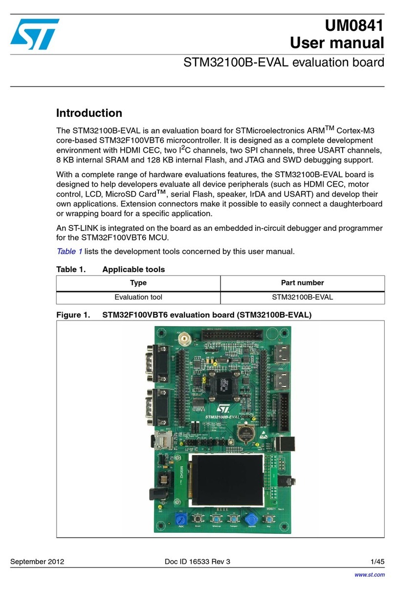
The STM32100B-EVAL is an evaluation board for STMicroelectronic’s ARMTM Cortex-M3
core-based STM32F100VBT6 microcontroller. It is designed as a complete development
environment with HDMI CEC, two I2C channels, two SPI channels, three USART channels,
8 KB internal SRAM and 128 KB internal Flash, and JTAG and SWD debugging support.
With a complete range of hardware evaluations features, the STM32100B-EVAL board is
designed to help developers evaluate all device peripherals (such as HDMI CEC, motor
control, LCD, MicroSD Card™, serial Flash, speaker, IrDA and USART) and develop their
own applications. Extension connectors make it possible to easily connect a daughterboard
or wrapping board for a specific application.
An ST-LINK is integrated on the board as an embedded in-circuit debugger and programmer
for the STM32F100VBT6 MCU.
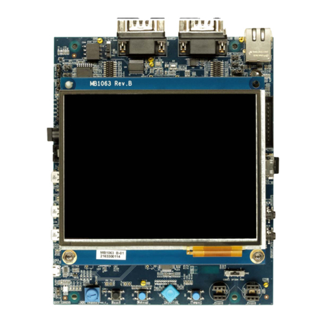
Figure 1. STM32F100VBT6 evaluation board (STM32100B-EVAL)
www.st.com
Downloaded from Elcodis.com electronic components distributor

Contents UM0841
2/41 Doc ID 16533 Rev 2
Contents
1 Overview . . . . . . . . . . . . . . . . . . . . . . . . . . . . . . . . . . . . . . . . . . . . . . . . . . 4
1.1 Features . . . . . . . . . . . . . . . . . . . . . . . . . . . . . . . . . . . . . . . . . . . . . . . . . . . 4
1.2 Demonstration software . . . . . . . . . . . . . . . . . . . . . . . . . . . . . . . . . . . . . . . 4
1.3 Order code . . . . . . . . . . . . . . . . . . . . . . . . . . . . . . . . . . . . . . . . . . . . . . . . . 4
2 Hardware layout and configuration . . . . . . . . . . . . . . . . . . . . . . . . . . . . . 5
2.1 Power supply . . . . . . . . . . . . . . . . . . . . . . . . . . . . . . . . . . . . . . . . . . . . . . . 7
2.2 Boot option . . . . . . . . . . . . . . . . . . . . . . . . . . . . . . . . . . . . . . . . . . . . . . . . . 8
2.3 Clock source . . . . . . . . . . . . . . . . . . . . . . . . . . . . . . . . . . . . . . . . . . . . . . . . 9
2.4 Reset source . . . . . . . . . . . . . . . . . . . . . . . . . . . . . . . . . . . . . . . . . . . . . . . 9
2.5 Audio . . . . . . . . . . . . . . . . . . . . . . . . . . . . . . . . . . . . . . . . . . . . . . . . . . . . . 9
2.6 Serial Flash . . . . . . . . . . . . . . . . . . . . . . . . . . . . . . . . . . . . . . . . . . . . . . . . 9
2.7 RS-232 . . . . . . . . . . . . . . . . . . . . . . . . . . . . . . . . . . . . . . . . . . . . . . . . . . . 10
2.8 Motor control . . . . . . . . . . . . . . . . . . . . . . . . . . . . . . . . . . . . . . . . . . . . . . 10
2.9 MicroSD Card . . . . . . . . . . . . . . . . . . . . . . . . . . . . . . . . . . . . . . . . . . . . . . 10
2.10 Temperature sensor . . . . . . . . . . . . . . . . . . . . . . . . . . . . . . . . . . . . . . . . . 10
2.11 Development and debug support . . . . . . . . . . . . . . . . . . . . . . . . . . . . . . . 10
2.12 Analog input . . . . . . . . . . . . . . . . . . . . . . . . . . . . . . . . . . . . . . . . . . . . . . . 11
2.13 IrDA . . . . . . . . . . . . . . . . . . . . . . . . . . . . . . . . . . . . . . . . . . . . . . . . . . . . . 11
2.14 Display and input devices . . . . . . . . . . . . . . . . . . . . . . . . . . . . . . . . . . . . . 11
2.15 IDD measurement . . . . . . . . . . . . . . . . . . . . . . . . . . . . . . . . . . . . . . . . . . 12
2.15.1 Run mode . . . . . . . . . . . . . . . . . . . . . . . . . . . . . . . . . . . . . . . . . . . . . . . 12
2.15.2 Low power mode . . . . . . . . . . . . . . . . . . . . . . . . . . . . . . . . . . . . . . . . . . 12
2.15.3 Standby or Stop IDD measurement procedure . . . . . . . . . . . . . . . . . . . 12
2.15.4 Low IDD measurement improvement procedure . . . . . . . . . . . . . . . . . . 13
2.16 HDMI CEC . . . . . . . . . . . . . . . . . . . . . . . . . . . . . . . . . . . . . . . . . . . . . . . . 13
3 Connectors . . . . . . . . . . . . . . . . . . . . . . . . . . . . . . . . . . . . . . . . . . . . . . . 14
3.1 Audio jack CN1 . . . . . . . . . . . . . . . . . . . . . . . . . . . . . . . . . . . . . . . . . . . . . 14
3.2 JTAG debugging connector CN3 . . . . . . . . . . . . . . . . . . . . . . . . . . . . . . . 14
3.3 Daughterboard extension connectors CN4 and CN5 . . . . . . . . . . . . . . . . 15
3.4 Motor control connector CN6 . . . . . . . . . . . . . . . . . . . . . . . . . . . . . . . . . . 19
Downloaded from Elcodis.com electronic components distributor

UM0841 Contents
Doc ID 16533 Rev 2 3/41
3.5 Analog input connector CN7 . . . . . . . . . . . . . . . . . . . . . . . . . . . . . . . . . . 20
3.6 Power supply connector CN8 . . . . . . . . . . . . . . . . . . . . . . . . . . . . . . . . . . 20
3.7 RS-232 connector CN9 with RTS/CTS handshake support . . . . . . . . . . . 21
3.8 RS-232 connector CN10 with ISP support . . . . . . . . . . . . . . . . . . . . . . . . 21
3.9 MicroSD connector CN11 . . . . . . . . . . . . . . . . . . . . . . . . . . . . . . . . . . . . . 22
3.10 ST-LINK connector CN12 . . . . . . . . . . . . . . . . . . . . . . . . . . . . . . . . . . . . . 22
3.11 ST-LINK programming connector CN13 . . . . . . . . . . . . . . . . . . . . . . . . . . 23
3.12 HDMI connectors CN15 and CN16 . . . . . . . . . . . . . . . . . . . . . . . . . . . . . 23
4 Limitations . . . . . . . . . . . . . . . . . . . . . . . . . . . . . . . . . . . . . . . . . . . . . . . . 24
4.1 Boot switches . . . . . . . . . . . . . . . . . . . . . . . . . . . . . . . . . . . . . . . . . . . . . . 24
4.2 PE14, PB14 and PA10 usage . . . . . . . . . . . . . . . . . . . . . . . . . . . . . . . . . . 24
4.3 Jumper JP3 . . . . . . . . . . . . . . . . . . . . . . . . . . . . . . . . . . . . . . . . . . . . . . . 24
4.4 Audio amplifier volume . . . . . . . . . . . . . . . . . . . . . . . . . . . . . . . . . . . . . . . 24
4.5 IDD standby measurement . . . . . . . . . . . . . . . . . . . . . . . . . . . . . . . . . . . . 24
5 Schematics . . . . . . . . . . . . . . . . . . . . . . . . . . . . . . . . . . . . . . . . . . . . . . . 25
Appendix A STM32100B-EVAL I/O assignments . . . . . . . . . . . . . . . . . . . . . . . . . 37
Revision history . . . . . . . . . . . . . . . . . . . . . . . . . . . . . . . . . . . . . . . . . . . . . . . . . . . . 40
Downloaded from Elcodis.com electronic components distributor

Overview UM0841
4/41 Doc ID 16533 Rev 2
1 Overview
1.1 Features
●Three 5 V power supply options: power jack, ST-LINK connector or daughterboard
●Boot from user Flash, system memory or SRAM
●Speaker
●1 Gbyte MicroSD Card™
●16 Mbyte serial Flash
●I2C/SMBus compatible serial interface temperature sensor
●Two RS-232 communication channels with support for RTS/CTS handshake on one
channel
●IrDA transceiver
●Induction motor control connector
●JTAG and SWD debug support
●240x320 TFT color LCD
●Joystick with 4-direction control and selector
●Reset, wakeup, tamper and user push buttons
●Four LEDs
●RTC with backup battery
●Extension connector for daughterboard or wrapping board
●Embedded ST-LINK
●IDD current measurement circuit
●HDMI CEC
1.2 Demonstration software
Demonstration software is preloaded in the board's Flash memory for easy demonstration of
the device peripherals in stand-alone mode. For more information and to download the
latest version available, please refer to the STM32100B-EVAL demonstration software
available on www.st.com.
1.3 Order code
To order the STM32F100VBT6 evaluation board, use the order code STM32100B-EVAL.
Downloaded from Elcodis.com electronic components distributor

UM0841 Hardware layout and configuration
Doc ID 16533 Rev 2 5/41
2 Hardware layout and configuration
The STM32100B-EVAL board is designed around a STM32F100VBT6 microcontroller in a
100-pin LQFP package.
The hardware block diagram Figure 2 shows the connections between the
STM32F100VBT6 microcontroller and the peripherals (LCD, SPI Flash, USART, IrDA,
speaker, HDMI CEC, temperature sensor, MicroSD Card, motor control and embedded ST-
LINK).
Figure 3 will help you locate these features on the evaluation board.
Figure 2. Hardware block diagram
34-&6"4 23
TRANSCEIVER
)R$!
TRANSCEIVER
6REGULATOR
4&4COLOR
,#$
-ICRO3$
#ARD
3PEAKER
AMPLIFIER
".#
CONNECTOR
,%$S
0OTENTIOMETER
53!24
$"CONNECTOR
$!#
'0)/
)# %XTENSION
CONNECTORFOR
'0)/S
-#5
CONSUMPTION
MEASUREMENT
53!24
4EMPERATURE
SENSOR
*4!'
*OYSTICK
!$#
%MBEDDED
34,).+
53"4YPE"
CONNECTOR
"UTTONS
!$#
-OTOR#ONTROL
CONNECTOR -#
*4!'4RACE
CONNECTOR
53!24
$"CONNECTOR
30)
53!24
23
TRANSCEIVER
53!24
3ERIAL&LASH
30)
#%#
)#
($-)
CONNECTOR
($-)
CONNECTOR
Downloaded from Elcodis.com electronic components distributor

Hardware layout and configuration UM0841
6/41 Doc ID 16533 Rev 2
Figure 3. STM32100B-EVAL board layout
CN4, CN5
Extension connector
CN9
USART2
CN10
USART1
CN11
MicroSD
U14
IrDA
CN8
Power jack
RV2
Potentiometer B1
RESET B2
WAKEUP B3
Tamper U4
Joystick B4
Key
CN6
Motor control
CN16
HDMI
connector
CN15
HDMI
connector
CN3
JTAG
CN12
ST-LINK
U14
Color LCD
CN1
Audio jack
CN7
BNC
RV1
Potentiometer
U3
VALUELINE
Downloaded from Elcodis.com electronic components distributor

UM0841 Hardware layout and configuration
Doc ID 16533 Rev 2 7/41
2.1 Power supply
The STM32100B-EVAL board is designed to be powered by a 5 V DC power supply and to
be protected by PolyZen U10 in case of incorrect power supply configuration.
It is possible to configure the evaluation board to use any of the following sources for the
power supply:
●5 V DC power adapter connected to CN8, the power supply jack labeled “PSU” (for
power supply unit) on the silkscreen.
●5 V DC power with 500 mA limitation from CN12, the ST-LINK type-B USB connector
labeled “USB” on the silkscreen.
●5 V DC power from both CN4 and CN5, the daughterboard extension connectors
labeled “DTB” (for daughterboard) on the silkscreen.
The power supply is configured by setting jumpers JP9 and JP10 as described in Table 1.
To enable MCU power consumption measurement, JP8 and JP12 should be re-configured
as described in Table 2. (PCB rev B only. See Section 4.5: IDD standby measurement for
details.)
LED LD5 is lit when the STM32100B-EVAL board is correctly powered by 5 V.
Note: The AC220V to DC5V power adapter PSU-5V2A (recommended and can be ordered from
ST, it is not provided with board by default) or equivalent power adapter (polarity compatible
with CN8) can be used to power STM32100B-EVAL board via power jack CN8 on the board.
To order the recommended power supply, use the order code PSU-5C2A.
Table 1. Power jumpers
Jumper Description
JP10
JP10 is used to select one of the three possible power supply resources.
For power supply from the power supply jack (CN8) to the
STM32100B-EVAL only, JP10 is set as shown:
For power supply from the daughterboard connectors (CN4 and CN5)
to the STM32100B-EVAL only, JP10 is set as shown:
For power supply from the ST-LINK USB connector (CN12) to the
STM32100B-EVAL only, JP10 is set as shown (default setting):
For power supply from power supply jack (CN8) to both the
STM32100B-EVAL board and to a daughterboard connected on CN4
and CN5, JP10 is set as shown: The daughterboard must not have its
own power supply connected.
JP9
Vbat is connected to VDD_MCU power when JP9 is set as shown (default
setting):
Vbat is connected to battery when JP9 is set as shown:
PSU
DTB
USB
PSU
DTB
USB
PSU
DTB
USB
PSU
DTB
USB
1 2 3
1 2 3
Downloaded from Elcodis.com electronic components distributor

Hardware layout and configuration UM0841
8/41 Doc ID 16533 Rev 2
2.2 Boot option
The STM32100B-EVAL board can boot from:
●Embedded user Flash
●System memory with boot loader for ISP
●Embedded SRAM for debugging
The boot option is configured by switches SW1 and SW2 as shown in Table 3.
Note: The hardware implementation of JP4 and the RS-232 interface can be only used when the
Boot0 is at a high level through the onboard switch SW2, which is not the most common
case of usage.
Table 2. MCU power consumption measurement jumpers
Jumper Description
JP8
VDD power is directly connected to MCU VDD when JP8 is set as shown:
(Default setting)
Note: For manual IDD measurement JP8 must be removed and replaced by an ammeter
connected between JP8 pins 1 and 2.
Connect VDD power to MCU with current-sampling resistor, 1Ωor 1KΩ, in series
for IDD current measurement when JP8 is set as shown:
JP12 (Available only on PCB rev B.) Connect IDD_CNT_EN (PE14) to Anti-tamper (PC13) for
IDD current measurement in standby mode when JP12 is closed.
Default setting: Not fitted
1 2 3
1 2 3
Table 3. Boot switches and jumper
Switch Boot from Switch configuration
SW1
SW2
STM32100B-EVAL boots from user Flash when SW2 is set as
shown to the right (default setting).
In this configuration, the position of SW1 does not affect the boot
process.
STM32100B-EVAL boots from embedded SRAM when SW1 and
SW2 are set as shown to the right.
STM32100B-EVAL boots from system memory when SW1 and
SW2 are set as shown to the right.
JP4
BOOT0 pin of the STM32F100VBT6 is connected to the RS-232
connector CN10 pin 8 (CTS) for ISP support when JP4 is closed.
This configuration is used for boot loader application only.
Default setting: not fitted.
SW2
Boot
0
0 <--> 1
SW
1
Boot
1
SW2
Boot
0
0 <--> 10 <--> 1
SW2
Boot
0
SW1
Boot
1
Downloaded from Elcodis.com electronic components distributor

UM0841 Hardware layout and configuration
Doc ID 16533 Rev 2 9/41
2.3 Clock source
Two clock sources are available on the STM32100B-EVAL board for the STM32F100VBT6
microcontroller and RTC.
●X1, 32 KHz crystal for embedded RTC
●X2, 8 MHz crystal with socket for the STM32F100VBT6 microcontroller. It can be
removed from the socket when the internal RC clock is used.
2.4 Reset source
The reset signal of the STM32100B-EVAL board is active low and the reset sources include:
●Reset button B1
●Debugging tools from JTAG connector CN3
●Daughterboard from CN5
●Embedded ST-LINK
●Bootloader_Reset from RS-232 connector CN10
2.5 Audio
The STM32100B-EVAL board supports playback based on a speaker on the board. This
can be disabled or enabled by jumpers JP1 and JP2. The audio volume can be adjusted
using the potentiometer RV1. See Section 4.4: Audio amplifier volume.
2.6 Serial Flash
A 128 Mbit serial Flash connected to SPI1 of the STM32F100VBT6 microcontroller shares
the same SPI port with the MicroSD Card using a different chip select signal. Serial Flash
chip select is managed by the standard I/O port PD9.
Table 4. Reset jumper
Jumper Description
JP5
Bootloader_Reset signal from the RS-232 connector CN10 pin 1 (DCD) is connected
to RESET# of the STM32F100VBT6 when JP5 is closed.
This configuration is used for the boot loader application only.
Default setting: Not fitted
Table 5. Audio jumpers
Jumper Description
JP1 Audio power amplifier TS4990IST is forced on standby mode when JP1 is fitted.
Default setting: Not fitted
JP2 The DAC _OUT(PA4) is connected to speaker circuit when JP2 is closed.
Default setting: Fitted
Downloaded from Elcodis.com electronic components distributor

Hardware layout and configuration UM0841
10/41 Doc ID 16533 Rev 2
2.7 RS-232
Two type D 9-pin connectors, CN10 (USART1) and CN9 (USART2) are available on the
STM32100B-EVAL board.
●CN10 connects to the RS-232 transceiver U15 with Bootloader_Reset and
Bootloader_BOOT0 support.
●CN9 connects to the RS-232 transceiver U13 with RTS/CTS handshake signal support.
2.8 Motor control
The STM32100B-EVAL board supports induction motor control via a 34-pin connector, CN6,
which provides all required control and feedback signals to and from a motor power-drive
board. Available signals on this connector include emergency stop, motor speed, 3-phase
motor current, bus voltage, heat sink temperature coming from the motor drive board and 6
channels of PWM control signals going to the motor drive circuit.
Special motor current sampling operation is enabled by setting jumper JP7.
Note: On MB871 PCB rev A MC_CurrentA shares PC1 with VBAT_ADCIN through JP3 so the
jumper JP3 must be removed for motor control applications. See Section 4.3: Jumper JP3.
2.9 MicroSD Card
The 1 Gbyte MicroSD Card connected to SPI1 of the STM32F100VBT6 microcontroller
(shared with serial Flash), is available on the board. MicroSD Card chip selection is
managed by the standard I/O port PC12 while the MicroSD card defect signal is managed
by I/O port PE7.
2.10 Temperature sensor
One I2C interface temperature sensor STLM75 (–55°C to +125°C) connected to I2C1 of the
STM32F10x microcontroller, is available on the board.
2.11 Development and debug support
An embedded ST-LINK STM32 JTAG interface developed by STMicroelectronic’s is
available on the STM32100B-EVAL as the default debugger hardware interface.
Of course, third-party debugger interfaces are also supported by the JTAG connector CN3.
Table 6. Motor control jumpers
Jumper Description
JP7
The special motor current sampling operation is enabled when JP7 is fitted (PD2
connected to PB0). The I/O pins PD2 and PB0 are disconnected and can be used by
daughterboard when JP7 is not fitted.
Default setting: Not fitted
JP6 JP6 should be kept open when encoder signal is from pin 31 of motor control connector
CN6. It should be kept closed when analog signal is from pin 31 of CN6 for special motor.
Default setting: Not fitted (open)
Downloaded from Elcodis.com electronic components distributor

UM0841 Hardware layout and configuration
Doc ID 16533 Rev 2 11/41
2.12 Analog input
One BNC connector, CN7, is connected to PA4 of the STM32F100VBT6 microcontroller as
an external analog input. or DAC output. The 50Ωterminal resistor can be enabled by
closing solder bridge SB1. A low pass filter can be implemented for the BNC connector by
replacing R44 and C33 for ADC input, or replacing R43 and C33 for DAC output with the
correct value of resistor and capacitor as requested by the end user's application.
There are also 3 analog signals available on the board:
1. 10 KΩpotentiometer RV2 connected to PC4.
2. IDD measurement output signal connected to PC5 for MCU power consumption test.
3. External ADC input which can be connected to TP3 (AIN+) and TP2 (AIN-), R45 should
be removed to avoid noise.
2.13 IrDA
IrDA communication is supported by the IrDA transceiver U14, which is connected to
USART3 of the STM32F100VBT6 microcontroller. It is enabled or disabled by jumper JP11.
2.14 Display and input devices
The 240x320 TFT color LCD (mounted on connector CN14) and 4 general purpose LEDs
(LD1, 2, 3, 4) are available as display devices.
A 4-direction joystick with selection key, general purpose push button (B4), wakeup button
(B2) and tamper detection button (B3) are available as input devices.
Table 7. IrDA jumper
Jumper Description
JP11 Enables/disables the IrDA transceiver. IrDA is enabled when JP11 is fitted, and disabled
when JP11 is not fitted.
Default setting: Fitted
Table 8. 240x320 TFT color LCD modules
CN14 pin Description Pin connection CN14 pin Description Pin connection
1 CS PB2 9 VDD +3V3
2 SCL PB13 10 VCI +3V3
3 SDI PB15 11 GND GND
4RS 12GND GND
5WR 13BL_VDD +3V3
6 RD 14 BL_Control PA8
7 SDO PB14 15 BL_GND GND
8 RESET# RESET# 16 BL_GND GND
Downloaded from Elcodis.com electronic components distributor

Hardware layout and configuration UM0841
12/41 Doc ID 16533 Rev 2
2.15 IDD measurement
For IDD measurement the circuit below is implemented on the STM32100B-EVAL.
Figure 4. STM32100B-EVAL IDD measurement circuit
2.15.1 Run mode
In Run mode, IDD current is measured using MAX9938FEUK+ (U6) connected to the 1Ω
shunt resistor (R71). In this case IDD_CNT_EN remains high during measurement and a
jumper must be connected between pins 2 and 3 of JP8.
2.15.2 Low power mode
In low power modes (Stop or Standby), the operational amplifier MAX9938FEUK+ (U6) is
connected to the 1KΩshunt resistor (R72), controlled by the analogue switch STT5PF20V
(T2). In this case the counter 74HC4060 (U9) enabled by IDD_CNT_EN manages the
measurement timing according to Figure 5.
2.15.3 Standby or Stop IDD measurement procedure
To measure a current corresponding to the low power mode the procedure is:
1. Configure ADC to measure voltage on IDD_measurement pin.
2. Configure PA0 as wakeup pin.
3. Enter in Low Power mode after configuring IDD_CNT_EN Low as output low level
(PC13 if JP12 is closed, or PE14 if JP12 is open or on MB871 rev A).
4. LP_WAKEUP rising edge wakeup the MCU after around 150 ms.
5. Start ADC conversion as soon as possible after wakeup in order to measure the
voltage corresponding to Low Power mode on capacitor C41.
6. Reset the counter by programming IDD_CNT_EN High in less than 70 ms after the
wakeup to avoid 1 KΩbeing connected later on VDD_MCU.
Downloaded from Elcodis.com electronic components distributor

UM0841 Hardware layout and configuration
Doc ID 16533 Rev 2 13/41
In low power mode, the 1 KΩresistor is connected when T2 goes off after entering low
power mode. Q13 output of the counter allows connection of the 1KΩresistor when the
current IDD becomes very low. The measurement timing is given in Figure 5.
Figure 5. STM32100B-EVAL IDD low power mode measurement timing diagram
The low power mode measurement procedure can be used in Standby or Stop mode if the
IDD current does not exceed 60 uA, otherwise the Run mode measurement procedure
should be used up to 60 mA.
Note: 1 The standby current measure is not possible on MB871 rev A as explained in chapter 3.5
IDD standby measure.
2 In standby mode the bias current of operational amplifier input (U6 pin 4) is not negligible
compared to IDD current (Typical I bias is ~200 nA). To improve the IDD measurement
precision it mandatory to subtract the I bias current to the IDD standby measure since this
current is not sink by the MCU. It is possible to measure I bias (U1 pin 4 current) and to
subtract this value to MCU current.
2.15.4 Low IDD measurement improvement procedure
The procedure for precision IDD measurement is:
1. Place a jumper on JP8 pins 1 and 2.
2. Follow the low power mode procedure to measure I1 = I bias.
3. Remove jumper JP8 pins 1 and 2 and place it on JP8 pins 2 and 3.
4. Follow the low power mode procedure to measure I2 = IDD + I bias.
5. Calculate actual IDD: IDD = I2 - I1.
2.16 HDMI CEC
Two HDMI connectors CN15 and CN16 are available on the STM32100B-EVAL board. The
signals CEC, SCL, SDA and HPD are supported and connected to the STM32F100VBT6
through HDMI2C1-5DIJ, the ST full integrated ESD protection, level-shifting device and
signal booster for control links of the HDMI 1.3 transmitter.
0 150mS 300mS 450mS
MC U mo d e
Run
Low power
Wake-up IDD Measure
Low pow er mode IDD measurement timing
Q14 = L P_WAK EUP
Clear CNT
IDD_CNT_EN
Q13 = LOW_POWER_EN
(T2 pin 3)
Q14n = U7 pin 4
Table 9. HDMI CEC solder bridge
Jumper Description
SB4 The +5 V power pin of HDMI connectors CN15 and CN16 is connected to 5 V power on the
STM32100B-EVAL board when SB4 is closed. Default status: Open
Downloaded from Elcodis.com electronic components distributor

Connectors UM0841
14/41 Doc ID 16533 Rev 2
3 Connectors
3.1 Audio jack CN1
A 3.5 mm mono audio jack CN1 is available on the STM32100B-EVAL board. The speaker
U12 is bypassed when earphones are plugged into CN8.
3.2 JTAG debugging connector CN3
Figure 6. JTAG debugging connector CN3 (front view)
Table 10. JTAG debugging connector
Pin number Description Pin number Description
1 3.3V power 2 3.3V power
3TRST 4GND
5TDI 6GND
7 TMS/SWDIO 8 GND
9 TCK/SWCLK 10 GND
11 RTCK 12 GND
13 TDO/SWO 14 GND
15 RESET# 16 GND
17 Pull-Down 18 GND
19 Pull-Down 20 GND
19 17 15 13 11 9 7 5 3 1
20 18 16 14 12 10 8 6 4 2
Downloaded from Elcodis.com electronic components distributor

UM0841 Connectors
Doc ID 16533 Rev 2 15/41
3.3 Daughterboard extension connectors CN4 and CN5
Two 50-pin male headers, CN4 and CN5, can connect a daughterboard or standard
wrapping board to the STM32100B-EVAL board. All GPIOs are available on these
connectors. The space between these two connectors and position of power, GND and
RESET pin is defined as a standard (which allows to develop common daughterboards for
several evaluation boards). Moreover all I/O on these connectors are pinout compatible with
the STM3210B-EVAL board (except PC14 and PC15 which do not exist on the
STM32F103VBT6). The standard width between CN4 pin1 and CN5 pin1 is 2700 mils
(68.58mm). The standard was implemented on the majority of evaluation boards. Each pin
on CN4 and CN5 can be used by a daughterboard after disconnecting it from the
corresponding function block on the STM32100B-EVAL board. Refer to Table 11 and
Table 12 for details.
Table 11. Daughterboard extension connector CN4
Pin Description Alternate function How to disconnect from function block on
STM32100B-EVAL board
1GND - -
3 PC1 MC connector pin15 Disconnect STM32100B-EVAL evaluation board
from motor power drive board
5 PC3 MC connector pin 19 Disconnect STM32100B-EVAL evaluation board
from motor power drive board
7 PA1 MC connector pin 33 Disconnect STM32100B-EVAL evaluation board
from motor power drive board
9 PA3 MC connector pin 14 Disconnect STM32100B-EVAL evaluation board
from motor power drive board
11 PA4 Audio_DAC / BNC Keep JP2 on open
13 PA6 SPI Flash& MicroSD card Remove R89
15 PC4 Potentiometer RV2 Remove R48
17 PB0 MC connector pin 27 Keep JP7 on open
19 GND - -
21 PE7 MicroSD card detect Remove card from CN11 or remove R91
23 PE9 MC connector pin 3 Disconnect STM32100B-EVAL evaluation board
from motor power drive board
25 PE11 MC connector pin 7 Disconnect STM32100B-EVAL evaluation board
from motor power drive board
27 PE13 MC connector pin 11 Disconnect STM32100B-EVAL evaluation board
from motor power drive board
29 PE15 MC connector pin 1 Remove R24
31 PC14 OSC32_IN Keep SB2 on close and remove R17
33 PB10 HDMI_SCL Remove R108
35 PB13 LCD_CLK -
37 PB15 LCD_MOSI -
39 GND - -
Downloaded from Elcodis.com electronic components distributor

Connectors UM0841
16/41 Doc ID 16533 Rev 2
41 PD9 Flash_CS -
43 PD11 - -
45 PD13 MC connector pin 23 Disconnect STM32100B-EVAL evaluation board
from motor power drive board
47 PD15 - -
49 D5V - -
2 PC0 MC connector pin 26 Disconnect STM32100B-EVAL evaluation board
from motor power drive board
4 PC2 MC connector pin 17 Disconnect STM32100B-EVAL evaluation board
from motor power drive board
6PA0 MC connector pin 31 &
Wakeup button
Disconnect STM32100B-EVAL evaluation board
from motor power drive board.
Remove R58
8 PA2 MC connector pin 34 Disconnect STM32100B-EVAL evaluation board
from motor power drive board
10 GND - -
12 PA5 SPI Flash & MicroSD card -
14 PA7 SPI Flash & MicroSD card -
16 PC5 IDD_measurement Remove R70
18 PB1 MC connector pin 29 Disconnect STM32100B-EVAL evaluation board
from motor power drive board
20 PB2 BOOT1 & LCD -
22 PE8 MC connector pin 5 Disconnect STM32100B-EVAL evaluation board
from motor power drive board
24 PE10 MC connector pin 9 Disconnect STM32100B-EVAL evaluation board
from motor power drive board
26 PE12 MC connector pin 13 Disconnect STM32100B-EVAL evaluation board
from motor power drive board
28 PE14 IDD_CNT_EN Remove R117 (does not exist on PCB rev A)
30 GND - -
32 PC15 OSC32_OUT Keep SB3 on close and remove R17
34 PB11 HDMI_SDA Remove R109
36 PB12 HDMI_HPD Remove R110
38 PB14 LCD_MISO Remove R116 (does not exist on PCB rev A)
40 PD8 Joystick Up Remove R42
42 PD10 MC connector pin 21 Disconnect STM32100B-EVAL evaluation board
from motor power drive board
44 PD12 Joystick selection Remove R38
Table 11. Daughterboard extension connector CN4 (continued)
Pin Description Alternate function How to disconnect from function block on
STM32100B-EVAL board
Downloaded from Elcodis.com electronic components distributor

UM0841 Connectors
Doc ID 16533 Rev 2 17/41
46 PD14 Joystick Down Remove R39
48 +3V3 - -
50 GND - -
Table 12. Daughterboard extension connector CN5
Pin Description Alternate function How to disconnect from component on
STM32100B-EVAL board
1GND - -
3NC -
5 PE6 - -
7 PE4 - -
9 PC13 Tamper Key Remove R37
11 RESET# RESET# button -
13 PE1 Joystick Right Remove R41
15 PB9 User button Remove R46
17 PB7 Temperature sensor_SDA Remove R47
19 D5V - -
21 PB4 Debug nTRST -
23 NC - -
25 PD6 USART2_RX Remove R81
27 PD4 USART2_RTS Remove R15
29 PD3 USART2_CTS Remove R82
31 PD1 - -
33 PC12 MicroSD card_CS Remove R90
35 PC10 IrDA_TX -
37 PA14 Debug TCK/SWCLK -
39 GND - -
41 PA12 - -
43 PA10 USART1_RX Remove R115 (not existent on PCB rev A)
45 PA8 MCO -
47 PC8 LED3 Remove R61
49 PC6 LED1 Remove R59
2NC
4 PC13 Tamper button Remove R637
Table 11. Daughterboard extension connector CN4 (continued)
Pin Description Alternate function How to disconnect from function block on
STM32100B-EVAL board
Downloaded from Elcodis.com electronic components distributor

Connectors UM0841
18/41 Doc ID 16533 Rev 2
6 PE5 - -
8 PE3 - -
10 GND - -
12 PE2 - -
14 PE0 Joystick Left Remove R40
16 PB8 HDMI_CEC Remove R107
18 PB6 Temperature sensor_SCL Remove R49
20 PB5 Temperature sensor_INT Remove R50
22 PB3 Debug TDO/SWO -
24 NC - -
26 PD7 - -
28 PD5 USART2 Remove R9
30 GND - -
32 PD2 MC connector pin 27 Disconnect STM32100B-EVAL evaluation board
from motor power drive board.
Keep JP7 on open
34 PD0 - -
36 PC11 IrDA_RX Remove R83
38 PA15 Debug TDI -
40 PA13 Debug TMS/SWDIO -
42 PA11 LCD_Backlight -
44 PA9 USART1_TX Remove R16
46 PC9 LED4 Remove R62
48 PC7 LED2 Remove R60
50 GND - -
Table 12. Daughterboard extension connector CN5 (continued)
Pin Description Alternate function How to disconnect from component on
STM32100B-EVAL board
Downloaded from Elcodis.com electronic components distributor

UM0841 Connectors
Doc ID 16533 Rev 2 19/41
3.4 Motor control connector CN6
Figure 7. Motor control connector CN6 (top view)
Table 13. Motor control connector CN6
Description STM32F100VBT6
pin CN6
pin STM32F100VBT6
pin Description
Emergency stop PE15 1 2 GND
PWM-UH PE9 3 4 GND
PWM-UL PE8 5 6 GND
PWM-VH PE11 7 8 GND
PWM-VL PE10 9 10 GND
PWM-WH PE13 11 12 GND
PWM-WL PE12 13 14 PA3 Bus voltage
PHASE A current PC1 15 16 GND
PHASE B current PC2 17 18 GND
PHASE C current PC3 19 20 GND
NTC bypass relay PD10 21 22 GND
Dissipative brake PWM PD13 23 24 GND
+5 V power 25 26 PC0 Heatsink temperature
PFC SYNC PD2/PB0 27 28 3.3 V power
PFC PWM PB1 29 30 GND
Encoder A PA0 31 32 GND
Encoder B PA1 33 34 PA2 Encoder index
33 31 29 27 25 23 21 19 17 15 13 11 9 7 5 3 1
34 32 30 28 26 24 22 20 18 16 14 12 10 8 6 4 2
Downloaded from Elcodis.com electronic components distributor

Connectors UM0841
20/41 Doc ID 16533 Rev 2
3.5 Analog input connector CN7
Figure 8. Analog input connector CN7 (bottom view)
3.6 Power supply connector CN8
The STM32100B-EVAL board can be powered from a DC 5 V power supply via the external
power supply jack (CN8) shown in Figure 9. The central pin of CN8 must be positive.
Figure 9. Power supply connector CN8 (front view)
Table 14. Analog input connector CN7
Pin number Description Pin number Description
1GND 4GND
2 GND 5 Analog input/PA4
3GND
1
4
5
3
2
DC +5V
GND
Downloaded from Elcodis.com electronic components distributor
Other manuals for STM32100B-EVAL
3
Table of contents
Other ST Motherboard manuals

ST
ST STM32L476G-EVAL User manual

ST
ST UM2335 User manual

ST
ST STM32H743I-EVAL User manual

ST
ST STEVAL-IFS001V1 User manual

ST
ST STM32G4 Nucleo-32 User manual

ST
ST STEVAL-IDB011V1 User manual

ST
ST AEK-MOT-TK200G1 User manual

ST
ST STCC50x1 User manual

ST
ST EVALSP320SCPU User manual

ST
ST STM32F407 Series User manual