ST STM32756G-EVAL User manual

March 2016 DocID027919 Rev 2 1/79
1
UM1903
User manual
Evaluation board with STM32F756NG MCU
Introduction
The STM32756G-EVAL evaluation board is a complete demonstration and development
platform for STMicroelectronics ARM®Cortex®-M7 core-based STM32F756NGH6
microcontroller. It features four I2C interfaces, six SPIs with three multiplexed simplex I2S
interfaces, SDMMC, four USARTs, four UARTs, two CANs, three 12-bit ADCs, two 12-bit
DACs, two SAIs, 8 to 14-bit digital camera module interface, internal 320+4-Kbyte SRAM
and 1-Mbyte Flash memory, USB HS OTG and USB FS OTG, Ethernet MAC, FMC
interface, Quad-SPI interface, cryptographic hardware accelerator, JTAG debugging
support. This evaluation board can be used as a reference design for user application
development but it is not considered as a final application.
The full range of hardware features on the board helps the user to evaluate all peripherals
(USB OTG HS, USB OTG FS, Ethernet, Motor control, CAN, microSD card, USART, Audio
DAC and ADC, digital microphone, IrDA, RF-EEPROM, SRAM, Nor Flash memory,
SDRAM, Quad-SPI Flash memory, 5.7" TFT LCD with a capacitive touch panel and others)
and to develop his applications. Extension headers make it possible to easily connect a
daughterboard for a specific application.
The integrated ST-LINK/V2-1 provides an embedded in-circuit debugger and programmer
for the STM32.
Figure 1. STM32756G-EVAL evaluation board
1. Picture not contractual.
www.st.com

Contents UM1903
2/79 DocID027919 Rev 2
Contents
1 Features . . . . . . . . . . . . . . . . . . . . . . . . . . . . . . . . . . . . . . . . . . . . . . . . . . . 7
2 Demonstration software . . . . . . . . . . . . . . . . . . . . . . . . . . . . . . . . . . . . . . 8
3 Ordering information . . . . . . . . . . . . . . . . . . . . . . . . . . . . . . . . . . . . . . . . 8
4 Delivery recommendations . . . . . . . . . . . . . . . . . . . . . . . . . . . . . . . . . . . 8
5 Hardware layout and configuration . . . . . . . . . . . . . . . . . . . . . . . . . . . . . 9
5.1 Embedded ST-LINK/V2-1 . . . . . . . . . . . . . . . . . . . . . . . . . . . . . . . . . . . . . 10
5.1.1 Drivers . . . . . . . . . . . . . . . . . . . . . . . . . . . . . . . . . . . . . . . . . . . . . . . . . . 11
5.1.2 ST-LINK/V2-1 firmware upgrade . . . . . . . . . . . . . . . . . . . . . . . . . . . . . . 11
5.2 Power supply . . . . . . . . . . . . . . . . . . . . . . . . . . . . . . . . . . . . . . . . . . . . . . 12
5.3 Clock source . . . . . . . . . . . . . . . . . . . . . . . . . . . . . . . . . . . . . . . . . . . . . . . 15
5.4 Reset source . . . . . . . . . . . . . . . . . . . . . . . . . . . . . . . . . . . . . . . . . . . . . . 16
5.5 Boot option . . . . . . . . . . . . . . . . . . . . . . . . . . . . . . . . . . . . . . . . . . . . . . . . 17
5.6 Audio . . . . . . . . . . . . . . . . . . . . . . . . . . . . . . . . . . . . . . . . . . . . . . . . . . . . 17
5.7 USB OTG FS1 . . . . . . . . . . . . . . . . . . . . . . . . . . . . . . . . . . . . . . . . . . . . . 20
5.8 USB OTG HS and USB OTG FS2 . . . . . . . . . . . . . . . . . . . . . . . . . . . . . . 20
5.9 RS232 and IrDA . . . . . . . . . . . . . . . . . . . . . . . . . . . . . . . . . . . . . . . . . . . . 21
5.10 MicroSD card . . . . . . . . . . . . . . . . . . . . . . . . . . . . . . . . . . . . . . . . . . . . . . 21
5.11 RF-EEPROM . . . . . . . . . . . . . . . . . . . . . . . . . . . . . . . . . . . . . . . . . . . . . . 22
5.12 CAN . . . . . . . . . . . . . . . . . . . . . . . . . . . . . . . . . . . . . . . . . . . . . . . . . . . . . 22
5.13 Ethernet . . . . . . . . . . . . . . . . . . . . . . . . . . . . . . . . . . . . . . . . . . . . . . . . . . 22
5.14 Memories . . . . . . . . . . . . . . . . . . . . . . . . . . . . . . . . . . . . . . . . . . . . . . . . . 23
5.15 Quad-SPI Nor Flash memory . . . . . . . . . . . . . . . . . . . . . . . . . . . . . . . . . . 24
5.16 Analog input . . . . . . . . . . . . . . . . . . . . . . . . . . . . . . . . . . . . . . . . . . . . . . . 24
5.17 Camera module . . . . . . . . . . . . . . . . . . . . . . . . . . . . . . . . . . . . . . . . . . . . 24
5.18 Display and input devices . . . . . . . . . . . . . . . . . . . . . . . . . . . . . . . . . . . . . 25
5.19 Motor control . . . . . . . . . . . . . . . . . . . . . . . . . . . . . . . . . . . . . . . . . . . . . . 27
5.20 MFX (Multi-Function eXpander) . . . . . . . . . . . . . . . . . . . . . . . . . . . . . . . . 28

DocID027919 Rev 2 3/79
UM1903 Contents
4
6 Connector . . . . . . . . . . . . . . . . . . . . . . . . . . . . . . . . . . . . . . . . . . . . . . . . 30
6.1 Motor control connector CN1 . . . . . . . . . . . . . . . . . . . . . . . . . . . . . . . . . . 30
6.2 RF-EEPROM daughterboard connector CN2 . . . . . . . . . . . . . . . . . . . . . 31
6.3 Analog input connector CN3 . . . . . . . . . . . . . . . . . . . . . . . . . . . . . . . . . . 31
6.4 Camera module connector CN4 . . . . . . . . . . . . . . . . . . . . . . . . . . . . . . . . 32
6.5 Daughterboard extension connector CN5 and CN6 . . . . . . . . . . . . . . . . . 33
6.6 RS232 connector CN7 . . . . . . . . . . . . . . . . . . . . . . . . . . . . . . . . . . . . . . . 37
6.7 USB OTG HS Micro-AB connector CN8 . . . . . . . . . . . . . . . . . . . . . . . . . 38
6.8 Ethernet RJ45 connector CN9 . . . . . . . . . . . . . . . . . . . . . . . . . . . . . . . . . 38
6.9 Memory connector CN10 and CN11 . . . . . . . . . . . . . . . . . . . . . . . . . . . . 39
6.10 ETM Trace debugging connector CN12 . . . . . . . . . . . . . . . . . . . . . . . . . . 42
6.11 USB OTG FS1 Micro-AB connector CN13 . . . . . . . . . . . . . . . . . . . . . . . . 42
6.12 USB OTG FS2 Micro-AB connector CN14 . . . . . . . . . . . . . . . . . . . . . . . . 43
6.13 JTAG/SWD connector CN15 . . . . . . . . . . . . . . . . . . . . . . . . . . . . . . . . . . 43
6.14 MicroSD connector CN16 . . . . . . . . . . . . . . . . . . . . . . . . . . . . . . . . . . . . . 44
6.15 Power connector CN17 . . . . . . . . . . . . . . . . . . . . . . . . . . . . . . . . . . . . . . 45
6.16 ST-LINK/V2-1 programming connector CN18 . . . . . . . . . . . . . . . . . . . . . 45
6.17 MFX programming connector CN19 . . . . . . . . . . . . . . . . . . . . . . . . . . . . . 45
6.18 TFT LCD connector CN20 . . . . . . . . . . . . . . . . . . . . . . . . . . . . . . . . . . . . 45
6.19 ST-LINK/V2-1 USB Type B connector CN21 . . . . . . . . . . . . . . . . . . . . . . 46
6.20 CAN D-type 9-pin male connector CN22 . . . . . . . . . . . . . . . . . . . . . . . . . 46
6.21 MEMS microphone coupon connectors CN24 and CN27 . . . . . . . . . . . . 47
6.22 Audio jack (speaker) CN25 . . . . . . . . . . . . . . . . . . . . . . . . . . . . . . . . . . . 47
6.23 Audio jack CN26 . . . . . . . . . . . . . . . . . . . . . . . . . . . . . . . . . . . . . . . . . . . . 47
6.24 SPDIF IN connector CN28 . . . . . . . . . . . . . . . . . . . . . . . . . . . . . . . . . . . . 48
Appendix A Electrical schematics . . . . . . . . . . . . . . . . . . . . . . . . . . . . . . . . . . . . 49
Appendix B STM32756G-EVAL I/O assignment . . . . . . . . . . . . . . . . . . . . . . . . . . 68
Appendix C Mechanical dimensions. . . . . . . . . . . . . . . . . . . . . . . . . . . . . . . . . . . 76
Appendix D Compliance statement. . . . . . . . . . . . . . . . . . . . . . . . . . . . . . . . . . . . 77
D.1 Federal Communications Commission (FCC) and Industry
Canada (IC) Compliance Statements . . . . . . . . . . . . . . . . . . . . . . . . . . . . 77

Contents UM1903
4/79 DocID027919 Rev 2
D.1.1 FCC Compliance Statement . . . . . . . . . . . . . . . . . . . . . . . . . . . . . . . . . . 77
Part 15.19 . . . . . . . . . . . . . . . . . . . . . . . . . . . . . . . . . . . . . . . . . . . . . . . . . . . . . . .77
Part 15.105 . . . . . . . . . . . . . . . . . . . . . . . . . . . . . . . . . . . . . . . . . . . . . . . . . . . . . .77
Part 15.21 . . . . . . . . . . . . . . . . . . . . . . . . . . . . . . . . . . . . . . . . . . . . . . . . . . . . . . .77
D.2 IC Compliance Statement . . . . . . . . . . . . . . . . . . . . . . . . . . . . . . . . . . . . . 77
D.2.1 Compliance Statement . . . . . . . . . . . . . . . . . . . . . . . . . . . . . . . . . . . . . . 77
D.2.2 Déclaration de conformité. . . . . . . . . . . . . . . . . . . . . . . . . . . . . . . . . . . . 77
7 Revision History . . . . . . . . . . . . . . . . . . . . . . . . . . . . . . . . . . . . . . . . . . . 78

DocID027919 Rev 2 5/79
UM1903 List of tables
5
List of tables
Table 1. Power related jumpers . . . . . . . . . . . . . . . . . . . . . . . . . . . . . . . . . . . . . . . . . . . . . . . . . . . . 13
Table 2. 25 MHz Crystal X1 related solder bridges . . . . . . . . . . . . . . . . . . . . . . . . . . . . . . . . . . . . . 16
Table 3. 32KHz Crystal X2 related solder bridges . . . . . . . . . . . . . . . . . . . . . . . . . . . . . . . . . . . . . . 16
Table 4. Boot related switch . . . . . . . . . . . . . . . . . . . . . . . . . . . . . . . . . . . . . . . . . . . . . . . . . . . . . . . 17
Table 5. Boot related jumpers. . . . . . . . . . . . . . . . . . . . . . . . . . . . . . . . . . . . . . . . . . . . . . . . . . . . . . 17
Table 6. Audio related jumpers. . . . . . . . . . . . . . . . . . . . . . . . . . . . . . . . . . . . . . . . . . . . . . . . . . . . . 18
Table 7. USB OTG FS2 function configuration. . . . . . . . . . . . . . . . . . . . . . . . . . . . . . . . . . . . . . . . . 20
Table 8. USART1 related jumpers . . . . . . . . . . . . . . . . . . . . . . . . . . . . . . . . . . . . . . . . . . . . . . . . . . 21
Table 9. CAN related jumpers . . . . . . . . . . . . . . . . . . . . . . . . . . . . . . . . . . . . . . . . . . . . . . . . . . . . . 22
Table 10. Ethernet related jumpers . . . . . . . . . . . . . . . . . . . . . . . . . . . . . . . . . . . . . . . . . . . . . . . . . . 23
Table 11. Ethernet related solder bridges. . . . . . . . . . . . . . . . . . . . . . . . . . . . . . . . . . . . . . . . . . . . . . 23
Table 12. NOR Flash memory related jumpers . . . . . . . . . . . . . . . . . . . . . . . . . . . . . . . . . . . . . . . . . 24
Table 13. LED related jumpers . . . . . . . . . . . . . . . . . . . . . . . . . . . . . . . . . . . . . . . . . . . . . . . . . . . . . . 25
Table 14. LCD modules connector (CN20). . . . . . . . . . . . . . . . . . . . . . . . . . . . . . . . . . . . . . . . . . . . . 25
Table 15. Motor control related solder bridges . . . . . . . . . . . . . . . . . . . . . . . . . . . . . . . . . . . . . . . . . . 28
Table 16. MFX signals . . . . . . . . . . . . . . . . . . . . . . . . . . . . . . . . . . . . . . . . . . . . . . . . . . . . . . . . . . . . 28
Table 17. Motor control connector CN1 . . . . . . . . . . . . . . . . . . . . . . . . . . . . . . . . . . . . . . . . . . . . . . . 30
Table 18. RF-EEPROM daughterboard connector CN2. . . . . . . . . . . . . . . . . . . . . . . . . . . . . . . . . . . 31
Table 19. Analog input-output connector CN3 . . . . . . . . . . . . . . . . . . . . . . . . . . . . . . . . . . . . . . . . . . 31
Table 20. Camera module connector CN4 . . . . . . . . . . . . . . . . . . . . . . . . . . . . . . . . . . . . . . . . . . . . . 32
Table 21. Daughterboard extension connector CN5 . . . . . . . . . . . . . . . . . . . . . . . . . . . . . . . . . . . . . 33
Table 22. Daughterboard extension connector CN6 . . . . . . . . . . . . . . . . . . . . . . . . . . . . . . . . . . . . . 35
Table 23. RS232 connector CN7 with ISP support. . . . . . . . . . . . . . . . . . . . . . . . . . . . . . . . . . . . . . . 37
Table 24. USB OTG HS Micro-AB connector CN8 . . . . . . . . . . . . . . . . . . . . . . . . . . . . . . . . . . . . . . . 38
Table 25. RJ45 connector CN9 . . . . . . . . . . . . . . . . . . . . . . . . . . . . . . . . . . . . . . . . . . . . . . . . . . . . . 38
Table 26. Memory connector CN10 . . . . . . . . . . . . . . . . . . . . . . . . . . . . . . . . . . . . . . . . . . . . . . . . . . 39
Table 27. Memory connector CN11 . . . . . . . . . . . . . . . . . . . . . . . . . . . . . . . . . . . . . . . . . . . . . . . . . . 40
Table 28. ETM Trace debugging connector CN12 . . . . . . . . . . . . . . . . . . . . . . . . . . . . . . . . . . . . . . . 42
Table 29. USB OTG FS1 Micro-AB connector CN13 . . . . . . . . . . . . . . . . . . . . . . . . . . . . . . . . . . . . . 43
Table 30. USB OTG FS2 Micro-AB connector CN14 . . . . . . . . . . . . . . . . . . . . . . . . . . . . . . . . . . . . . 43
Table 31. JTAG/SWD debugging connector CN15 . . . . . . . . . . . . . . . . . . . . . . . . . . . . . . . . . . . . . . 44
Table 32. MicroSD connector CN16 . . . . . . . . . . . . . . . . . . . . . . . . . . . . . . . . . . . . . . . . . . . . . . . . . . 44
Table 33. USB type B connector CN21 . . . . . . . . . . . . . . . . . . . . . . . . . . . . . . . . . . . . . . . . . . . . . . . 46
Table 34. CAN D-type 9-pin male connector CN22 . . . . . . . . . . . . . . . . . . . . . . . . . . . . . . . . . . . . . . 46
Table 35. MEMS microphone coupon connectors CN24 and CN27. . . . . . . . . . . . . . . . . . . . . . . . . . 47
Table 36. SPDIF IN connector CN28 . . . . . . . . . . . . . . . . . . . . . . . . . . . . . . . . . . . . . . . . . . . . . . . . . 48
Table 37. I/O assignment . . . . . . . . . . . . . . . . . . . . . . . . . . . . . . . . . . . . . . . . . . . . . . . . . . . . . . . . . . 68
Table 38. Mechanical dimensions . . . . . . . . . . . . . . . . . . . . . . . . . . . . . . . . . . . . . . . . . . . . . . . . . . . 76
Table 39. Document Revision History . . . . . . . . . . . . . . . . . . . . . . . . . . . . . . . . . . . . . . . . . . . . . . . . 78

List of figures UM1903
6/79 DocID027919 Rev 2
List of figures
Figure 1. STM32756G-EVAL evaluation board . . . . . . . . . . . . . . . . . . . . . . . . . . . . . . . . . . . . . . . . . . 1
Figure 2. Hardware Block Diagram . . . . . . . . . . . . . . . . . . . . . . . . . . . . . . . . . . . . . . . . . . . . . . . . . . . 9
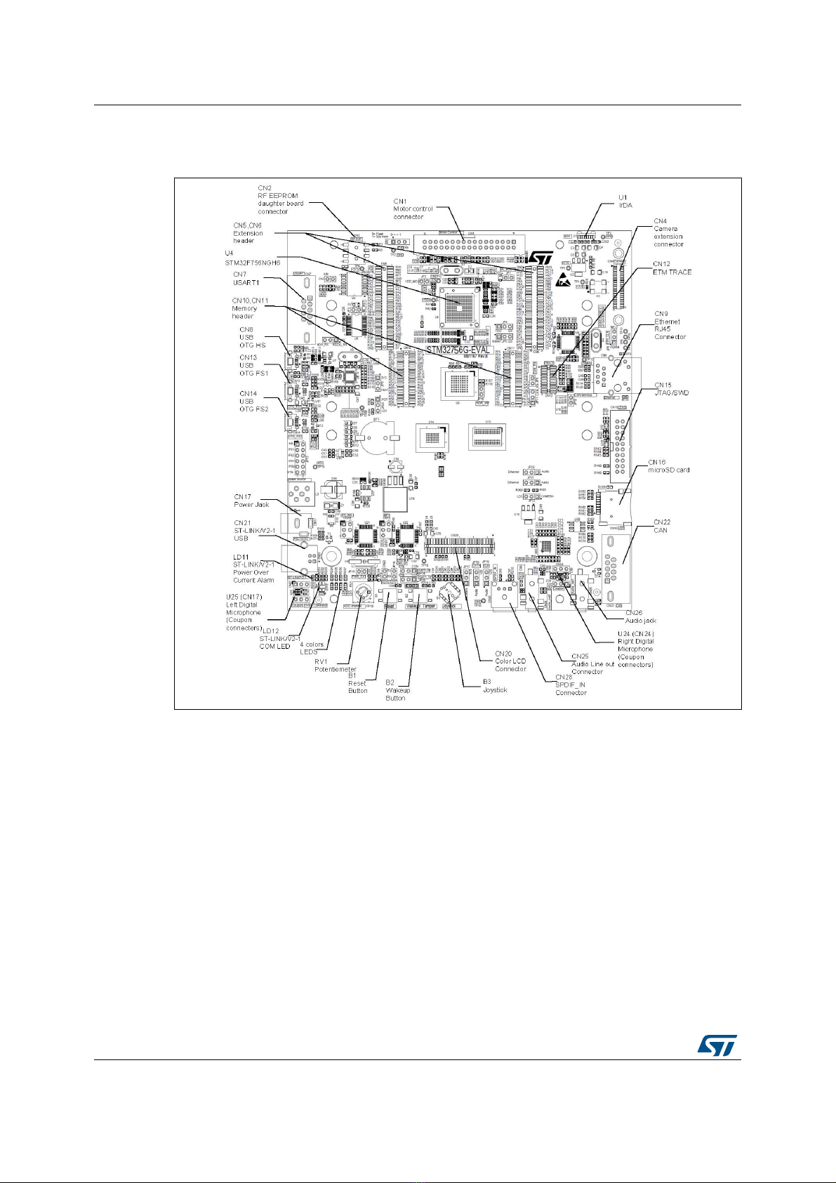
Figure 3. STM32756G-EVAL evaluation board layout. . . . . . . . . . . . . . . . . . . . . . . . . . . . . . . . . . . . 10
Figure 4. USB composite device . . . . . . . . . . . . . . . . . . . . . . . . . . . . . . . . . . . . . . . . . . . . . . . . . . . . 11
Figure 5. Orientation setting of the 5.7-inch LCD daughterboard . . . . . . . . . . . . . . . . . . . . . . . . . . . 26
Figure 6. STM32756G-EVAL evaluation board motor control PCB
reworks (Bottom side) . . . . . . . . . . . . . . . . . . . . . . . . . . . . . . . . . . . . . . . . . . . . . . . . . . . . . 27
Figure 7. STM32756G-EVAL evaluation board motor control PCB
reworks (Top side) . . . . . . . . . . . . . . . . . . . . . . . . . . . . . . . . . . . . . . . . . . . . . . . . . . . . . . . 28
Figure 8. Motor control connector CN1 (Top view) . . . . . . . . . . . . . . . . . . . . . . . . . . . . . . . . . . . . . . 30
Figure 9. RF-EEPROM daughterboard connector CN2 (Front view) . . . . . . . . . . . . . . . . . . . . . . . . . 31
Figure 10. Analog input-output connector CN3 (Top view) . . . . . . . . . . . . . . . . . . . . . . . . . . . . . . . . . 31
Figure 11. Camera module connector CN4 (Top view) . . . . . . . . . . . . . . . . . . . . . . . . . . . . . . . . . . . . 32
Figure 12. RS232 connector CN7 (Front view) . . . . . . . . . . . . . . . . . . . . . . . . . . . . . . . . . . . . . . . . . . 37
Figure 13. USB OTG HS Micro-AB connector CN8 (Front view) . . . . . . . . . . . . . . . . . . . . . . . . . . . . . 38
Figure 14. Ethernet RJ45 connector CN9 (Front view) . . . . . . . . . . . . . . . . . . . . . . . . . . . . . . . . . . . . 38
Figure 15. ETM Trace debugging connector CN12 (Top view) . . . . . . . . . . . . . . . . . . . . . . . . . . . . . . 42
Figure 16. USB OTG FS1 Micro-AB connector CN13 (Front view) . . . . . . . . . . . . . . . . . . . . . . . . . . . 42
Figure 17. USB OTG FS2 Micro-AB connector CN14 (Front view) . . . . . . . . . . . . . . . . . . . . . . . . . . . 43
Figure 18. JTAG/SWD debugging connector CN15 (Top view). . . . . . . . . . . . . . . . . . . . . . . . . . . . . . 43
Figure 19. MicroSD connector CN16 (Top view) . . . . . . . . . . . . . . . . . . . . . . . . . . . . . . . . . . . . . . . . . 44
Figure 20. Power supply connector CN17 (Front view) . . . . . . . . . . . . . . . . . . . . . . . . . . . . . . . . . . . 45
Figure 21. USB type B connector CN21 (Front view) . . . . . . . . . . . . . . . . . . . . . . . . . . . . . . . . . . . . . 46
Figure 22. CAN D-type 9-pin male connector CN22 (Front view) . . . . . . . . . . . . . . . . . . . . . . . . . . . . 46
Figure 23. MEMS microphone coupon connectors CN24 and CN27 (Top view). . . . . . . . . . . . . . . . . 47
Figure 24. SPDIF IN connector CN28 (Front view) . . . . . . . . . . . . . . . . . . . . . . . . . . . . . . . . . . . . . . . 48
Figure 25. STM32756G-EVAL evaluation board . . . . . . . . . . . . . . . . . . . . . . . . . . . . . . . . . . . . . . . . . 49
Figure 26. STM32756G-EVAL MCU . . . . . . . . . . . . . . . . . . . . . . . . . . . . . . . . . . . . . . . . . . . . . . . . . . 50
Figure 27. STM32756G-EVAL Power . . . . . . . . . . . . . . . . . . . . . . . . . . . . . . . . . . . . . . . . . . . . . . . . . 51
Figure 28. STM32756G-EVAL SRAM, Flash memory and DRAM . . . . . . . . . . . . . . . . . . . . . . . . . . . 52
Figure 29. STM32756G-EVAL Audio . . . . . . . . . . . . . . . . . . . . . . . . . . . . . . . . . . . . . . . . . . . . . . . . . 53
Figure 30. STM32756G-EVAL LCD, Camera and RF connector. . . . . . . . . . . . . . . . . . . . . . . . . . . . . 54
Figure 31. STM32756G-EVAL Ethernet . . . . . . . . . . . . . . . . . . . . . . . . . . . . . . . . . . . . . . . . . . . . . . . 55
Figure 32. STM32756G-EVAL USB OTG HS and OTG FS2 . . . . . . . . . . . . . . . . . . . . . . . . . . . . . . . 56
Figure 33. STM32756G-EVAL USB OTG FS1 . . . . . . . . . . . . . . . . . . . . . . . . . . . . . . . . . . . . . . . . . . 57
Figure 34. STM32756G-EVAL RS232 and IrDA . . . . . . . . . . . . . . . . . . . . . . . . . . . . . . . . . . . . . . . . . 58
Figure 35. STM32756G-EVAL CAN and QSPI . . . . . . . . . . . . . . . . . . . . . . . . . . . . . . . . . . . . . . . . . . 59
Figure 36. STM32756G-EVAL Peripherals . . . . . . . . . . . . . . . . . . . . . . . . . . . . . . . . . . . . . . . . . . . . . 60
Figure 37. STM32756G-EVAL Motor control . . . . . . . . . . . . . . . . . . . . . . . . . . . . . . . . . . . . . . . . . . . . 61
Figure 38. STM32756G-EVAL Extension connector . . . . . . . . . . . . . . . . . . . . . . . . . . . . . . . . . . . . . . 62
Figure 39. STM32756G-EVAL ST-LINK/V2-1 . . . . . . . . . . . . . . . . . . . . . . . . . . . . . . . . . . . . . . . . . . . 63
Figure 40. STM32756G-EVAL MFX . . . . . . . . . . . . . . . . . . . . . . . . . . . . . . . . . . . . . . . . . . . . . . . . . . 64
Figure 41. STM32756G-EVAL JTAG and Trace . . . . . . . . . . . . . . . . . . . . . . . . . . . . . . . . . . . . . . . . . 65
Figure 42. STM32756G-EVAL Camera daughterboard . . . . . . . . . . . . . . . . . . . . . . . . . . . . . . . . . . . . 66
Figure 43. STM32756G-EVAL 5.7 TFT LCD daughterboard . . . . . . . . . . . . . . . . . . . . . . . . . . . . . . . . 67
Figure 44. Mechanical dimensions . . . . . . . . . . . . . . . . . . . . . . . . . . . . . . . . . . . . . . . . . . . . . . . . . . . 76

DocID027919 Rev 2 7/79
UM1903 Features
78
1 Features
•STM32F756NGH6 microcontroller with 1-Mbyte Flash memory and 320+4-Kbyte RAM
•Six 5 V power supply options:
–Powerjack
– ST-LINK/V2-1 USB connector
– User USB HS connector
– User USB FS1 connector
– User USB FS2 connector
– Daughterboard
•SAI Audio DAC, stereo audio jack which supports headset with microphone
•Stereo digital microphone, audio jack connector used to connect external speakers
•2-Gbyte (or more) SDMMC interface microSD card
•RF-EEPROM on I2C compatible serial interface
•RS232 communication
•IrDA transceiver
•JTAG/SWD and ETM trace debug support
•Embedded ST-LINK/V2-1
•IEEE-802.3-2002 compliant Ethernet connector
•Camera module
•8Mx32-bit SDRAM, 1Mx16-bit SRAM and 8Mx16-bit Nor Flash memory
•512-Mbit Quad-SPI Nor Flash memory
•5.7-inch 640x480-pixel TFT color LCD with touch panel
•Joystick with 4-direction control and selector
•Reset, WakeUp/Tamper or key button
•4-color user LEDs
•Extension connectors and memory connectors for daughterboard or wrapping board
•USB OTG HS and FS with Micro-AB connectors
•RTC with backup battery
•CAN2.0 A/B compliant connection
•Potentiometer
•Motor control connector

Demonstration software UM1903
8/79 DocID027919 Rev 2
2 Demonstration software
Demonstration software is preloaded in the Flash memory of the STM32F756NGH6 MCU
for easy demonstration of the device peripherals in stand-alone mode. For more information
and to download the latest version available, refer to the STM32756G-EVAL demonstration
software available on www.st.com.
3 Ordering information
To order the evaluation board for STM32F756NGH6 MCU, use the order code:
STM32756G-EVAL2.
4 Delivery recommendations
Some verifications are needed before using the evaluation board for the first time, to make
sure that nothing was damaged during shipment and that no components are unplugged or
lost. When the board is extracted from its plastic bag, check that no component remains in
the bag.
The main components to verify are:
•The 25MHz crystal (X1) and 25MHz crystal (X4), which may have been removed from
its socket by a shock
•The microSD card, which may have been ejected from the connector CN16 (right side
of the board)
•The dual-interface EEPROM board (ANT7-M24LR-A), which may have been
unplugged from the connector CN2 (top left corner of the board)
Caution: There is an explosion risk, if the battery is replaced by an incorrect one.

DocID027919 Rev 2 9/79
UM1903 Hardware layout and configuration
78
5 Hardware layout and configuration
STM32756G-EVAL evaluation board is designed around the STM32F756NGH6 (216-pin
TFBGA package) MCU. The hardware block diagram Figure 2: Hardware Block Diagram
illustrates the connection between STM32F756NGH6 MCU and peripherals (SDRAM,
SRAM, Nor Flash memory, QSPI Flash memory, Camera module, Color LCD, USB OTG
connectors, Motor control connector, USART, IrDA, Ethernet, Audio, CAN, RF-EEPROM,
microSD card and embedded ST-LINK/V2-1).
Figure 2. Hardware Block Diagram
1. The red circles show the I/O shared among the default functions and the camera or
the motor control connectors.
06Y9
06[[[[[9
670)1*+
9%DWWHU\
$XGLR'$&DQG
DPSOLILHU
57&
3+<DQG(WKHUQHW
FRQQHFWRU
-7$*DQG7UDFH
FRQQHFWRU '$3
93RZHU
6XSSO\
56'%
FRQQHFWRU
.+]&U\VWDO
9%$7
,5'$
67/,1.9
,&
86%FRQQHFWRU
6:DQG7UDFH
FRQQHFWRU 73,8
0RWRUFRQWURO
FRQQHFWRU
0,,
6$,
5)(3520RU
$&3RQ
FRQQHFWRU
/&'
9*$/&'
,2BH[SDQGHU
-R\VWLFN7RXFK
VFUHHQ
0LFUR6'FDUG &$1FRQQHFWRU
&$1
.H\:DNHXS
7DPSHUEXWWRQV
*3,2
3RWHQWLRPHWHU
$'&
6'00&
+63+<86%
FRQQHFWRU
27*
125)ODVK
65$0
)0&
&DPHUD
FRQQHFWRU
'&0,
6'5$0
463, )ODVK
63',)B5; $XGLR,1
27*
)6 86%FRQQHFWRU
8$57

Hardware layout and configuration UM1903
10/79 DocID027919 Rev 2
Figure 3 will help the user to locate all these features on the actual evaluation board.
Figure 3. STM32756G-EVAL evaluation board layout
5.1 Embedded ST-LINK/V2-1
The ST-LINK/V2-1 programming and debugging tool is embedded on the STM32756G-
EVAL evaluation board. Compared to ST-LINK/V2 the changes are listed below.
The new features supported on ST-LINK/V2-1 are:
•USB software re-enumeration
•Virtual Com Port interface on USB
•Mass storage interface on USB
•USB power management request for more than 100 mA power on USB
This feature is no more supported on ST-LINK/V2-1:
•SWIM interface
For all general information concerning debugging and programming features common
between ST-LINK/V2 and ST-LINK/V2-1 refer to ST-LINK/V2 User Manual UM1075.

DocID027919 Rev 2 11/79
UM1903 Hardware layout and configuration
78
Note: ETM can only work at 50 MHz clock by default, because ETM signals are shared with other
peripherals. If a better performance of ETM is required (84 MHz/98 MHz), R31, R34, R35,
R37, R39, R247, SB4, SB16, SB18 must be removed, to reduce the stub on ETM signals. In
this configuration SAI, Ethernet and Camera are not functional and Nor Flash memory and
SRAM addresses are limited on A18.
5.1.1 Drivers
The ST-LINK/V2-1 requires a dedicated USB driver, which can be found on www.st.com for
Windows 7 and 8. On Windows XP the ST-LINK/V2-1 driver requires WinUsb to be installed
before using the ST-LINK/V2-1 (either available from Microsoft website or included in the
USB driver for ST-LINK/V2 for XP).
In case the STM32756G-EVAL evaluation board is connected to the PC, before the driver is
installed, some STM32756G-EVAL interfaces may be declared as “Unknown” in the PC
device manager. In this case the user must install the driver files, and update the driver of
the connected device from the device manager.
Note: Prefer using the “USB Composite Device” handle for a full recovery.
Figure 4. USB composite device
5.1.2 ST-LINK/V2-1 firmware upgrade
The ST-LINK/V2-1 embeds a firmware upgrade mechanism for in-situ upgrade through the
USB port. As the firmware may evolve during the life time of the ST-LINK/V2-1 product (for
example new functionalities, bug fixes, support for new microcontroller families), it is
recommended to visit www.st.com before starting to use the STM32756G-EVAL board and
periodically, in order to stay up-to-date with the latest firmware version.

Hardware layout and configuration UM1903
12/79 DocID027919 Rev 2
5.2 Power supply
STM32756G-EVAL evaluation board is designed to be powered by 5 V DC power supply
and it is protected by PolyZen from wrong power plug-in event. It is possible to configure the
evaluation board to use any of the following six sources for the power supply:
•5 V DC power adapter connected on the board to the power jack CN17, the power jack
on the board (Power Supply Unit on silk screen of JP13 (PSU)). This is default setting
of power supply source selection on STM32756G-EVAL evaluation board.
•5 V DC power with 300 mA limitation from CN21, the USB type B connector of
ST-LINK/V2-1 (USB 5 V power source on silkscreen of JP13 (STlk)). If the USB
enumeration succeeds (as explained below), the ST-LINK/V2-1 U5V power is enabled,
by asserting the PWR_EN pin. This pin is connected to a power switch (ST890), which
powers the board. This power switch features also a current limitation to protect the PC
in case of short-circuit on board. If an overcurrent (more than 600 mA) happens on the
board, the LED LD11 is lit. This setting cannot be used as default power source
selection, because the whole board power consumption will be larger than the current
limitation of DC power from CN21.
•5V DC power with 500 mA limitation from CN8, the USB OTG HS Micro-AB connector
(USB 5V power source on silkscreen of JP13 (HS)).
•5V DC power with 500 mA limitation from CN13, the USB OTG FS1 Micro-AB
connector (USB 5V power source on silkscreen of JP13 (FS1)).
•5V DC power with 500 mA limitation from CN14, the USB OTG FS2 Micro-AB
connector (USB 5V power source on silkscreen of JP13 (FS2)).
•5V DC power from CN5 and CN6, the extension connectors for daughterboard
(daughterboard power source on silkscreen of JP13 (D5V)).
STM32756G-EVAL evaluation board can be powered from ST-LINK/V2-1 USB connector
CN21 (U5V), only when the 5.7" LCD is disconnected, otherwise power consumption
exceeds 300mA. When the board is connected to USB port only the ST-LINK/V2-1 is
powered for the USB enumeration, because host PC only provides 100 mA max to the
board at that time. During the USB enumeration, STM32756G-EVAL board requires 300 mA
power from the host PC. If the host PC is able to provide the required power, the
enumeration succeeds and the power transistor U17 (ST890) is switched ON, the red LED
LD10 is turned ON, thus STM32756G-EVAL evaluation board can consume no more than
300 mA of current. If the host PC is not able to provide the requested current, the
enumeration fails. Therefore the ST890 (U17) remains OFF so consequently 3.3 V domain
of the board and STM32 will not be powered. As a consequence, the red LED LD10 remains
turned OFF. In this case it is mandatory to use an external power supply as extra power
supply.
E5V (from PSU) or D5V must be used as external power supply, in case current
consumption of STM32756G-EVAL evaluation board exceeds the allowed current on USB.
In this condition it is still possible to use USB for communication, for programming or
debugging only, but it is mandatory to power the board, first using E5V or D5V, then
connecting the USB cable to the PC. Proceeding this way ensures that the enumeration
succeeds, thanks to the external power source.

DocID027919 Rev 2 13/79
UM1903 Hardware layout and configuration
78
The following power sequence procedure must be respected:
•Connect jumper JP13 for PSU or D5V side
•Check that JP15 is removed
•Connect the external power source to PSU or D5V (daughterboard mounted)
•Check red LED LD10 is turned ON
•Connect the PC to USB connector CN21
If this order is not respected, the board may be powered by VBUS first then E5V or D5V,
and the following risks may be encountered:
1. If more than 300 mA current is needed by the board, the PC may be damaged or
current can be limited by PC. As a consequence the board is not powered correctly.
2. 300 mA will be requested at enumeration (since JP15 must be OFF), so there is risk
that request is rejected and enumeration does not succeed if the PC cannot provide
such current. Consequently the board is not powered (the led LD10 remains OFF).
Note: In case the board is powered by an USB charger, there is no USB enumeration, so the led
LD10 remains set to OFF permanently and the board is not powered. Only in this specific
case the jumper JP15 needs to be set to ON, to allow the board to be powered anyway but
in any cases the current will be limited to 600 mA by U17 (ST890).
The power supply is configured by setting the related jumpers JP2, JP9 and JP13 as
described in Table 1.
Table 1. Power related jumpers
Jumper Description
JP2 JP2 is used to measure STM32 current consumption manually by multimeter.
Default setting: Fitted
JP9
Vbat is connected to +3.3 V when JP9 is set as shown to the right
(Default setting):
Vbat is connected to battery when JP9 is set as shown to the right:
JP13
JP13 is used to select one of the six possible power supply resources.
For power supply jack (CN17) to the STM32756G-EVAL only, JP13 is set as shown
to the right (Default setting):
+6
)6
)6
'9
368
67ON
069

Hardware layout and configuration UM1903
14/79 DocID027919 Rev 2
JP13
For power supply from USB connector of ST-LINK/V2-1 (CN21) to STM32756G-
EVAL only, JP13 is set as shown to the right:
For power supply from the daughterboard connectors (CN5 and CN6) to
STM32756G-EVAL only, JP13 is set as shown to the right:
For power supply from USB OTG FS2 (CN14) to STM32756G-EVAL only, JP13 is
set as shown to the right:
For power supply from USB OTG FS1 (CN13) to STM32756G-EVAL only, JP13 is
set as shown to the right:
Table 1. Power related jumpers (continued)
Jumper Description
+6
)6
)6
'9
368
67ON
069
+6
)6
)6
'9
368
67ON
069
+6
)6
)6
'9
368
67ON
069
+6
)6
)6
'9
368
67ON
069

DocID027919 Rev 2 15/79
UM1903 Hardware layout and configuration
78
The led LD10 is lit when the STM32756G-EVAL evaluation board is correctly powered by
the 5 V .
Note: In order to avoid the impact of USB PHY and Ethernet PHY and get precise results of
current consumption on JP2, the following cautions need to be taken into account:
1) Configure Ethernet PHY into Power Down Mode by setting low level of IO_Expander
(EXP_IO1)
2) Configure USB HS PHY into Low Power Mode (Register Address=04,bit 6 in USB PHY).
5.3 Clock source
Two clock sources are available on STM32756G-EVAL evaluation board for
STM32F756NGH6 MCU and RTC embedded. Three clock resources for camera, Ethernet
PHY and USB OTG PHY:
•X1, 25 MHz Crystal with socket for STM32F756NGH6 Microcontroller, it can be
removed from socket when internal RC clock is used
•X2, 32 KHz Crystal for embedded RTC
•X3, 24 MHz oscillator for camera module (Default on camera daughterboard)
•X4, 25 MHz Crystal with socket for Ethernet PHY
•X5, 24 MHz Crystal for USB OTG HS PHY
JP13
For power supply from USB OTG HS (CN8) to STM32756G-EVAL only, JP13 is set
as shown to the right:
For power supply from power supply jack(CN17) to both STM32756G-EVAL and
daughterboard connected on CN5 and CN6, JP13 is set as shown to the right
(daughterboard must not have its own power supply connected):
Table 1. Power related jumpers (continued)
Jumper Description
+6
)6
)6
'9
368
67ON
069
+6
)6
)6
'9
368
67ON
069

Hardware layout and configuration UM1903
16/79 DocID027919 Rev 2
T
Note: About the jumper JP6 for Ethernet clock, refer to Section 5.13: Ethernet.
5.4 Reset source
The reset signal of STM32756G-EVAL evaluation board is low active and the reset sources
include:
•Reset button B1
•Debugging Tools from JTAG/SWD connector CN15 and ETM trace connector CN12
•Daughterboard from CN5
•Embedded ST-LINK/V2-1
•RS232 connector CN7 for ISP
Note: The jumper JP3 has to be closed for RESET handled by the pin 8 of the RS232 connector
CN7 (CTS signal).
Table 2. 25 MHz Crystal X1 related solder bridges
Jumper Description
SB27
PH0 is connected to 25 MHz crystal when SB27 is open.
(Default setting)
PH0 is connected to extension connector CN5 when SB27 is closed. In such case
R19 must be removed to avoid disturbance due to the 25 MHz quartz.
SB28
PH1 is connected to 25MHz crystal when SB28 is open.
(Default setting)
PH1 is connected to extension connector CN5 when SB28 is closed. In such case
C23 and X1 must be removed to avoid disturbance due to the 25 MHz quartz.
Table 3. 32KHz Crystal X2 related solder bridges
Solder
Bridge Description
SB25
PC14 is connected to 32 KHz crystal when SB25 is open.
(Default setting)
PC14 is connected to extension connector CN6 when SB25 is closed. In such case
R18 must be removed to avoid disturbance due to the 32 Khz quartz.
SB26
PC15 is connected to 32 KHz crystal when SB26 is open.
(Default setting)
PC15 is connected to extension connector CN6 when SB26 is closed. In such case
R17 must be removed to avoid disturbance due to the 32 Khz quartz.

DocID027919 Rev 2 17/79
UM1903 Hardware layout and configuration
78
5.5 Boot option
STM32756G-EVAL evaluation board can boot from:
•Embedded User Flash memory
•System memory with boot loader for ISP
•Embedded SRAM for debugging
The boot option is configured by setting switch SW1 (BOOT) and the boot base address is
programmed in the BOOT_ADD0 and BOOT_ADD1 option bytes. The BOOT can be
configured also via RS232 connector CN7.
5.6 Audio
An audio codec WM8994ECS/R, with 4 DACs and 2 ADCs inside, is connected to SAI
interface of the STM32F756NGH6 microcontroller to support TDM feature on SAI port. This
feature is able to implement audio recording on digital microphone and analog microphone
and audio playback of different audio stream on headphone and lineout at the same time.
It communicates with STM32F756NGH6 microcontroller via I2C1 bus which is shared with
LCD, camera module, RF-EEPROM and MFX (Multi-Function eXpander).
The analog microphone on the headset is connected to ADC of WM8994ECS/R through the
audio jack connector CN26. External speakers can be connected to WM8994ECS/R via
audio jack connector CN25.
Two digital microphones (MEMs microphone) MP34DT01TR are on STM32756G-EVAL
evaluation board. They are able to be connected to either audio codec or I2S port of the
STM32F756NGH6 microcontroller, by setting the jumpers shown in Table 6. The coupon
Table 4. Boot related switch
Switch configuration Boot address
option bytes Boot space
BOOT_ADD0 [15:0]
STM32756G-EVAL boot from
BOOT_ADD0[15:0]
ST programmed value: Flash
memory on ITCM at 0x0020
0000 (Default setting).
BOOT_ADD1 [15:0]
STM32756G-EVAL boot from
BOOT_ADD1[15:0]
ST programmed value: System
bootloader at 0x0010 0000
Table 5. Boot related jumpers
Jumper Description
JP1
The Bootloader_BOOT is managed by pin 6 of connector CN7 (RS232 DSR signal)
when JP1 is closed. This configuration is used for boot loader application only.
Default setting: Not fitted
SW1
0<->1
SW1
0<->1

Hardware layout and configuration UM1903
18/79 DocID027919 Rev 2
connectors CN24 and CN27 can be used to support MEMS microphone evaluation board
STEVAL-MKI129V1 after removing SB20 and SB21.
An optical connector CN28, compatible with SPDIF spec, is implemented on STM32756G-
EVAL, to receive external audio data.
Table 6. Audio related jumpers
Jumper Description
JP18
Data signal on digital microphone is connected to audio codec when JP18 is set as
shown to the right (Default setting):
Data signal on digital microphone is connected to I2S port of the STM32F756NGH6
when JP18 is set as shown to the right (it is also needed to set JP5, according to this
table):
JP19
Clock signal on digital microphone is connected to audio codec when JP19 is set as
shown to the right (Default setting):
Clock signal on digital microphone is connected to timer output (PC7) of the
STM32F756NGH6, used to divide by two I2S clock, when JP19 is set as shown to
the right (it is also needed to set JP4 according to this table):
JP4
PB3 is as TDO/SWO signal when JP4 is set as shown to the right (Default setting):
PB3 (I2S Clock) is connected to Timer input (PC6) of the STM32F756NGH6, used
as microphone clock divider, when JP4 is set as shown to the right (it is also needed
to set JP19 according to this table):

DocID027919 Rev 2 19/79
UM1903 Hardware layout and configuration
78
Note: The I2C address of WM8994ECS/R is 0b0011010.
JP5
PD6 is as FMC_NWAIT signal when JP5 is set as shown to the right (Default
setting):
PD6 is connected to digital microphone as I2S data signal when JP5 is set as shown
to the right (it is also needed to set JP18 together according to this table):
JP17
Digital microphone power source is connected to +3.3 V power when JP17 is set as
shown to the right (Default setting):
Digital microphone power source is connected to MICBIAS1 from WM8994ECS/R
when JP17 is set as shown to the right:
JP21
PA2 is connected to SAI2_SCKB when JP21 is set as shown to the right (Default
setting):
PA2 is connected to MII_MDIO (Ethernet) when JP21 is set as shown to the right:
JP22
PC1 is connected to SAI1_SDA when JP22 is set as shown to the right (Default
setting):
PC1 is connected to MII_MDC (Ethernet) when JP22 is set as shown to the right:
Table 6. Audio related jumpers (continued)
Jumper Description

Hardware layout and configuration UM1903
20/79 DocID027919 Rev 2
5.7 USB OTG FS1
STM32756G-EVAL evaluation board supports USB OTG full speed communication via a
USB Micro-AB connector (CN13) and USB power switch (U11) connected to VBUS. The
evaluation board can be powered by this USB connection at 5 V DC with 500 mA current
limitation.
A green led LD7 will be lit in one of these cases:
•Power switch (U11) is ON and STM32756G-EVAL works as a USB host
•VBUS is powered by another USB host when STM32756G-EVAL works as a USB
device
The red led LD8 will be lit when overcurrent occurs.
Note 1 STM32756G-EVAL evaluation board should be powered by external power supply when
using OTG function.
Note 2 JP8 must be removed when using USB OTG FS as mentioned in Table 9.
5.8 USB OTG HS and USB OTG FS2
STM32756G-EVAL evaluation board supports USB OTG FS2:
•High speed communication via a USB Micro-AB connector (CN8), USB High speed
PHY (U8) for high speed function.
•Full speed communication via another USB Micro-AB connector (CN14)
The evaluation board can be powered by these USB connectors (CN8 or CN14) at 5 V DC
with 500 mA current limitation.
As several OTG FS2 signals are shared with OTG HS ULPI bus, some PCB reworks are
needed, when using OTG FS2 (CN14), as shown in Table 7.
An USB power switch (U7) is also connected on VBUS and provides power to either CN8
(with SB12 and SB15 closed and SB13 and SB14 open), or CN14 (with SB13 and SB14
closed and SB12 and SB15 open).
Green led LD5 (for CN8) or LD9 (for CN14) will be lit when either power switch (U7) is ON
and STM32756G-EVAL works as a USB host, or VBUS is powered by another USB host
when STM32756G-EVAL works as a USB device.
The red led LD6 will be lit when over-current occurs.
Note: STM32756G-EVAL evaluation board should be powered, by an external power supply when
using OTG function.
Table 7. USB OTG FS2 function configuration
Function Mount Remove
OTG HS-CN8 (Default) R109,R115,SB12,SB15 R259,SB13,SB14,SB51
OTG FS2-CN14 R259,SB13,SB14,SB51 R109,R115,SB12,SB15
Table of contents
Other ST Motherboard manuals

ST
ST STM32MP157F-EV1 User manual

ST
ST EVAL-L9177A User manual

ST
ST STM32 NUCLEO-F042K6 User manual

ST
ST STM32L073Z-EVAL User manual

ST
ST Nucleo STM32F302R8 User manual

ST
ST ST9 Series User manual

ST
ST STM32L4R9I-EVAL User manual

ST
ST SPC56B-DIS User manual

ST
ST X-NUCLEO-NFC03A1 User manual

ST
ST STEVAL-IHM011V1 User manual

ST
ST eMotion STEVAL-MKI109V1 User manual

ST
ST BlueNRG-LP User manual

ST
ST STLINK-V3SET User manual

ST
ST SPC560P-DISP User manual

ST
ST STM32303C-EVAL User manual

ST
ST EVALSP1340CPU User manual

ST
ST EVAL-RHRPMPOL01 User manual

ST
ST STEVAL-IFS012V1 User manual

ST
ST L9678-S-EVB User manual

ST
ST STEVAL-IDB007V Series User manual