Operating Instructions— 7A26
In the AC coupling position, the DC component of the
signal is blocked by acapacitor in the input circuit. The AC
coupling position provides the best display of signals with a
DC component much larger than the AC components. The
precharge feature should be used with large DC inputs. To
use this feature, first set the coupling to GND. Connect the
probe to the circuit and wait about two seconds for the
coupling capacitor to charge. Then set the coupling to AC.
The GND position provides aground reference at the
input of the amplifier without externally grounding the
input connectors. However, the signals connected to the
inputs are not grounded, and the same DC load is presented
to the signal source.
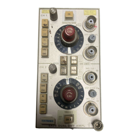
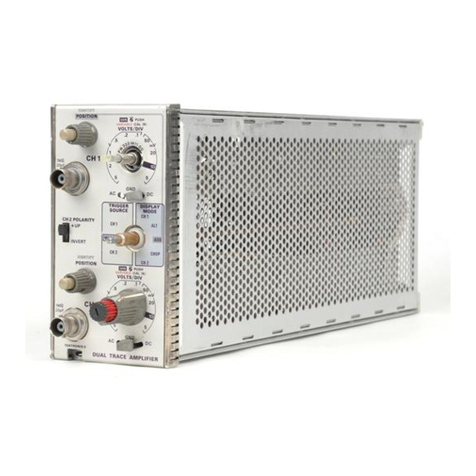
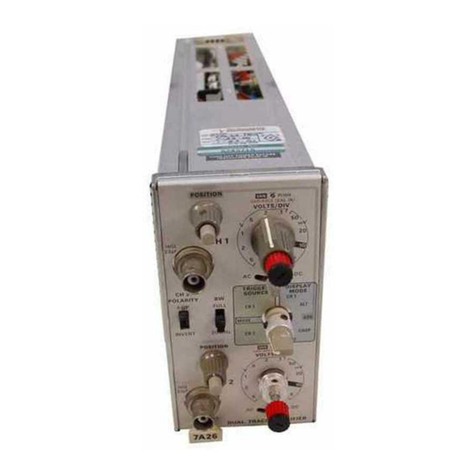
VOLTS/DIV and VARIABLE Controls
The amount of vertical deflection produced by asignal is
determined by the signal amplitude, the attenuation factor
of the probe, the setting of the VOLTS/DIV switch, and
the setting of the VARIABLE control. Calibration deflec-
tion factors indicated by the settings of the VOLTS/DIV
switch apply only when the VARIABLE control is in the
calibrated (CAL IN) position.
The VARIABLE control provides variable, uncalibrated
settings between the calibrated steps of the VOLTS/DIV
switch. With the VARIABLE control fully counter-
clockwise and the VOLTS/DIV set to 5volts/division the
uncalibrated vertical deflection factor is extended to at
least 12.5 volts/division. By applying acalibrated voltage
source to the input connector, any specific deflection
factor can be set within the range of the VARIABLE
control.
CH 2POLARITY Switch
The CH 2POLARITY switch may be used to invert the
displayed waveform of the signal applied to the CH 2input.
This is particularly useful in added operation of the 7A26
when differential measurements are to be made. The CH 2
POLARITY switch has two positions, +UP and INVERT. In
the +UP position, the displayed waveform will have the
same polarity as the applied signal and apositive DC voltage
will move the CRT trace up. In the INVERT position, a
positive-going waveform at the CH 2input will be displayed
on the CRT in inverted form and apositive DC voltage will
move the trace down.
DISPLAY MODE Switch
For single-trace operation, apply the signal either to the
CH 1input or the CH 2 input and set the DISPLAY MODE
switch to the corresponding position: CH 1or CH 2.
To display asignal in one channel independently when a
signal is also applied to the other channel, simply select the
desired channel by setting the DISPLAY MODE switch to
the appropriate CH 1or CH 2position.
Alternate Mode. The ALT position of the DISPLAY
MODE switch produces adisplay which alternates between
channel 1and channel 2with each sweep on the CRT.
Although the ALT mode can be used at all sweep rates, the
CHOP mode provides amore satisfactory display at sweep
rates below about 0.5 millisecond/division. At slow sweep
rates alternate mode switching becomes visually percep-
tible.
Add Mode. The ADD position of the DISPLAY MODE
switch can be used to display the sum or difference of two
signals, for common-mode rejection to remove an undesired
signal. The overall deflection factor in the ADD mode with
both VOLTS/DIV switches set to the same position is the
deflection factor indicated by either VOLTS/DIV switch.
However, if the CH 1and CH 2VOLTS/DIV switches are
set to different deflection factors, the resultant amplitude
is difficult to determine from the CRT display. In this case,
the voltage amplitude of the resultant display can be
determined accurately only if the amplitude of the signal
applied to one channel is known. In the ADD mode,
positioning of the trace is controlled by the channel 1
POSITION control only.
Chop Mode. The CHOP position of the DISPLAY
MODE switch produces adisplay which is electronically
switched between channels at approximately a500 kilo-
hertz rate (controlled by mainframe). In general the CHOP
mode provides the best display at sweep rates slower than
about 0.5 millisecond/division or whenever dual-trace,
non-repetitive phenomena is to be displayed.
TRIGGER SOURCE Switch
CH 1. The CH 1position of the TRIGGER SOURCE
switch provides atrigger signal obtained from the signal
applied to the CH 1input connector. This provides astable
display of the signal applied to the CH 1input connector.
CH 2. The CH 2position of the TRIGGER SOURCE
switch provides atrigger signal obtained from the signal
applied to the CH 2input connector. This provides astable
display of the signal applied to the CH 2input connector.
MODE. In this position of the TRIGGER SOURCE
switch, the trigger signal for the time-base unit is dependent
on the setting of the DISPLAY MODE switch. The trigger
REV. B, MAR. 1975 1-3
