TELink FR1 Instruction Manual

Telink FR1 PCB Design Guideline
AN-22051900-E1
Ver.1.0.0
2022/05/19
Keyword
Layout, FR1, PCB
Brief
This is Telink FR1 PCB design guideline which mainly introduces considerations when designing FR1 boards.

Telink FR1 PCB Design Guideline
AN-22051900-E1 Ver. 1.0.0
2
Published by
Telink Semiconductor
Bldg 3, 1500 Zuchongzhi Rd,
Zhangjiang Hi-Tech Park, Shanghai, China
© Telink Semiconductor
All Rights Reserved
Legal Disclaimer
This document is provided as-is. Telink Semiconductor reserves the right to make improvements without
further notice to this document or any products herein. This document may contain technical inaccuracies or
typographical errors. Telink Semiconductor disclaims any and all liability for any errors, inaccuracies or
incompleteness contained herein.
Copyright © 2022 Telink Semiconductor (Shanghai) Co. , Ltd.
Information
For further information on the technology, product and business term, please contact Telink Semiconductor
Company (www.telink-semi.com).
For sales or technical support, please send email to the address of:
telinksales@telink-semi.com
telinksupport@telink-semi.com

Telink FR1 PCB Design Guideline
AN-22051900-E1 Ver. 1.0.0
3
Revision History
Version Change Description Date Author
V1.0.0 Initial release. 2022/05 Junyao MAO,
Weixiang WANG

Telink FR1 PCB Design Guideline
AN-22051900-E1 Ver. 1.0.0
4
Table of Contents
Revision History ................................................................................................................................3
Table of Contents..............................................................................................................................4
List of Figures ...................................................................................................................................5
1. Overview ...................................................................................................................................6
2. Application Board Structure ID ...................................................................................................7
2.1 Single-layer board.................................................................................................................7
2.2 Doulbe-layer board ...............................................................................................................8
2.2.1 Component and copper wire layer + carbon film alignment layer ...........................................8
2.2.2 Component and copper wire layer + carbon film and copper wire layer...................................9
3. Key Points of FR1 Board Design................................................................................................ 10
3.1 Board layer ........................................................................................................................ 10
3.1.1 Board thickness selection ............................................................................................... 10
3.1.2 Introduction of board structure........................................................................................ 10
3.2 Carbon film routing ..............................................................................................................11
4. Layout Regulations................................................................................................................. 13
4.1 Package............................................................................................................................. 13
4.2 Solder pads and vias............................................................................................................ 13
4.3 Notes ................................................................................................................................ 15
5. Routing Notes........................................................................................................................ 18

Telink FR1 PCB Design Guideline
AN-22051900-E1 Ver. 1.0.0
5
List of Figures
Figure 2-1 Single-layer board........................................................................................................7
Figure 2-2 Component layer + carbon film layer ..............................................................................8
Figure 2-3 Double layer routing + carbon film routing ......................................................................9
Figure 3-1 Stack structure .......................................................................................................... 10
Figure 3-2 Carbon film routing.................................................................................................... 12
Figure 4-1 Package forms........................................................................................................... 13
Figure 4-2 Package design for Telink IC ....................................................................................... 14
Figure 4-3 Via hole on carbon film .............................................................................................. 15
Figure 4-4 Layout for RF circuit................................................................................................... 16
Figure 4-5 Layout for power capacitors ........................................................................................ 17
Figure 5-1 Routing example 1 ..................................................................................................... 19
Figure 5-2 Routing example 2 .................................................................................................... 19
Figure 5-3 Routing example 3 ....................................................................................................20

Telink FR1 PCB Design Guideline
AN-22051900-E1 Ver. 1.0.0
6
1. Overview
With the same PCB size and the same quantity of components, generally the fewer the number of PCB
layers, the more difficult the design.
Due to cost concern, PCB designs are increasingly preferred to use FR1 boards, single-layer boards, which
leads to more obvious problems in wireless communication, including power interference, RF high harmonics,
and etc.
This document uses the Telink SoC chips as a basis and the remote control design as an example to illustrate
how to guide the design of FR1 boards to achieve fast development and avoid multiple iterations.

Telink FR1 PCB Design Guideline
AN-22051900-E1 Ver. 1.0.0
7
2. Application Board Structure ID
According to the complexity of the components, taking into account cost and the difficulty of routing, the the
PCB design for Telink chips can be divided into single-layer boards or double-layer boards.
2.1 Single-layer board
In single-layer board design, make sure that all components and keys can be placed on the same side and
there should be enough space for the PCB antenna. This is suitable for boards with a small number of
components and routings.
The remote control board shown below can be designed as a single-layer board.
Figure 2-1 Single-layer board

Telink FR1 PCB Design Guideline
AN-22051900-E1 Ver. 1.0.0
8
2.2 Doulbe-layer board
2.2.1 Component and copper wire layer + carbon film routing layer
One layer of this double-layer board is used to place components and route copper wire, and the other layer
is for carbon film routing. For example, in a remote control design, we place the components on one layer
and the keys on the other layer. The keys need to be designed as carbon film keys and the keys routing is
connected to the component layer via carbon film via holes. Note that carbon film vias are chosen for cost
concerns.
The remote control board shown below can be designed as this type of double-layer board.
Figure 2-2 Component layer + carbon film layer

Telink FR1 PCB Design Guideline
AN-22051900-E1 Ver. 1.0.0
9
2.2.2 Component and copper wire layer + carbon film and copper wire layer
One layer of this double-layer board is used to place components and copper wire routing, and the other
layer is for carbon film routing + copper wire routing. For example, in a remote control design, we place the
components on one layer and the keys on the other layer. The keys need to be designed as carbon film keys
and the keys routing is connected to the component layer via carbon film via holes. When there are many
components and the routing is complex, if the design shown in 2.2.1 cannot be completed routing, then in
addition to the carbon film routing on another layer, it is necessary to add copper routing and connect the
component side routing through the carbon film via holes. Note that carbon film vias are chosen for cost
concerns.
The board shown below can be designed as this type of double-layer board.
Figure 2-3 Double layer routing + carbon film routing
Telink FR1 PCB Design Guideline
AN-22051900-E1 Ver. 1.0.0
10
3. Key Points of FR1 Board Design
3.1 Board layer
3.1.1 Board thickness selection
In order to reduce cost, FR1 or CEM-1 boards are generally used to produce PCB boards.
•The thickness of FR1 board is recommended to be 1.6mm.
•The thickness of CEM-1 board is recommended to be 1.2mm or 1.0mm.
Note:
1)
CEM-1 is more suitable for making thinner boards than FR1, and CEM-1 is less likely to warp boards
than FR1 over wave soldering.
2)
Whether FR1 or CEM-1 is used, the rules and notes for PCB design are the same.
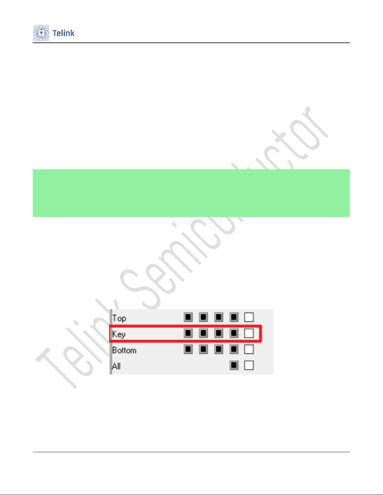
3.1.2 Introduction of board structure
In general, FR1 circuit board is single surface board, however, we need create another layer in addition to the
Top layer and Bottom layer, called the carbon film layer. As shown in the figure below, the Key layer is the
carbon film layer.
Figure 3-1 Stack structure
Table of contents
Other TELink Control Unit manuals

Popular Control Unit manuals by other brands

Festo
Festo Compact Performance CP-FB6-E Brief description

Elo TouchSystems
Elo TouchSystems DMS-SA19P-EXTME Quick installation guide

JS Automation
JS Automation MPC3034A user manual

JAUDT
JAUDT SW GII 6406 Series Translation of the original operating instructions

Spektrum
Spektrum Air Module System manual

BOC Edwards
BOC Edwards Q Series instruction manual

KHADAS
KHADAS BT Magic quick start

Etherma
Etherma eNEXHO-IL Assembly and operating instructions

PMFoundations
PMFoundations Attenuverter Assembly guide

GEA
GEA VARIVENT Operating instruction

Walther Systemtechnik
Walther Systemtechnik VMS-05 Assembly instructions

Altronix
Altronix LINQ8PD Installation and programming manual


