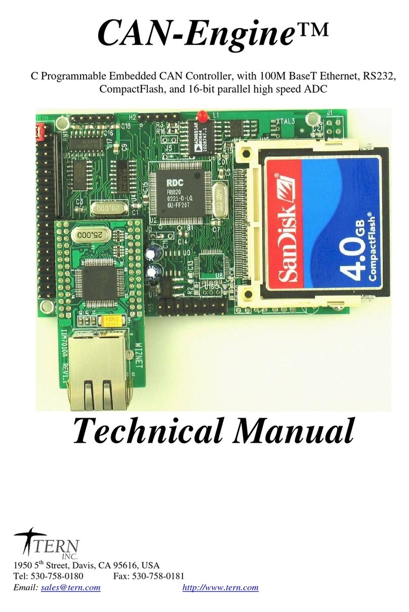
Tern R-Engine-D User manual

R-Engine-D™
16-bit Controller with 16-bit SRAM & Flash, Ethernet Interface,
Compact Flash interface with file system support, ADC/DAC
based on the 40MHz Am186ER or 80MHz RDC R1100
Technical Manual
1724 Picasso Avenue, Davis, CA 95616-0547, USA
Tel: 530-758-0180 Fax: 530-758-0181

COPYRIGHT
R-Engine, R-Engine-D, MemCard-A, MotionC, and ACTF are trademarks of TERN, Inc.
Am186ER is a trademark of Advanced Micro Devices, Inc.
Paradigm C/C++ is a trademark of Paradigm Systems.
Microsoft, MS-DOS, Windows, Windows95/98/2000/NT/XP are trademarks of
Microsoft Corporation.
IBM is a trademark of International Business Machines Corporation.
Version 1.00
May 27, 2003
No part of this document may be copied or reproduced in any form or by any means
without the prior written consent of TERN, Inc.
© 2002
1724 Picasso Avenue, Davis, CA 95616-0547, USA
Tel: 530-758-0180 Fax: 530-758-0181
Important Notice
TERN is developing complex, high technology integration systems. These systems are
integrated with software and hardware that are not 100% defect free. TERN products are
not designed, intended, authorized, or warranted to be suitable for use in life-support
applications, devices, or systems, or in other critical applications. TERN and the Buyer
agree that TERN will not be liable for incidental or consequential damages arising from
the use of TERN products. It is the Buyer's responsibility to protect life and property
against incidental failure.
TERN reserves the right to make changes and improvements to its products
without providing notice.

R-Engine-D Chapter 1: Introduction
Chapter 1: Introduction
1.1 Technical Manual Organization
This technical manual will require special organization to accommodate the possibility of configuring the
R-Engine-D with two different CPUs. The CPUs are very similar, yet they do have a few differences. For
purposes of organization, it will be assumed that throughout this technical manual, all information given is
accurate for both CPUs, unless otherwise stated. In general, it will be written referring to the Am186ER,
but will implicitly apply to the R1100 also. When information may deviate between CPUs, it will be
explicitly shown.
The rd.ide (tern\186) provides the user with sample and demos for hardware on the RD.
1.2 Functional Description
The R-Engine-D™ (RE) is a high performance, low cost, C/C++ programmable controller based on the
Am186ER CPU (40 MHz, 16-bit CPU, AMD). It is intended for industrial process control and high-speed
data acquisition, and especially ideal for OEM applications.The RE has 32KB internal RAM, which fulfills
many embedded OEM products SRAM requirement. No external SRAM would be required for an OEM
version of the RE (with Am186ER CPU only). This increases system reliability, while decreasing power
consumption and cost.
The RE features fast execution times through 16-bit ACTF Flash (256 KW) and battery-backed SRAM
(256 KW); it also includes 3 timers, PWMs, 32 PIOs, 24 PPIs, 512-byte serial EEPROM, an internal
UART, a sync serial port, 3 timer/counters, and a watchdog timer.
1-1
R-Engine-D
J5
8-pin
RJ45
50-pin Compact
Flash interface Supervisor
MAX691
512 byte
EEPROM
J4 Header – A/D Bus
J4 Header – A/D Bus
ADC
ADS 8344
8 chs.
ADC
AD7852
8 chs.
DAC
DA7625
4 chs.
J1 Header – A/D Bus
CS8900
Ethernet
controller
DAC
7612U
4 chs.
14 High
Voltage
Drivers
RTC
DS1337
PPI
24 TTL
I/Os
Dual UART
SC29C92
256KW
Flash
256KW
SRAM
Am186ER – 40MHz
OR
R1100 – 80MHz
3 16-bit timers/counters
6 external interrupts
1 Asynch / 1 Synch UART
32 I/O lines
PWM
16-bit external A/D bus

Chapter 1: Introduction R-Engine-D
Figure 1.1 Functional block diagram of the R-Engine-
The three 16-bit timers can be used to count or time external events, up to 10 MHz, 20MHz with the
R1100, or to generate non-repetitive or variable-duty-cycle waveforms as PWM outputs. The 32 PIO pins
from the Am186ER are multifunctional and user programmable.
A serial real time clock (DS1337, Dallas) is a low power clock/calendar with two time-of-day alarms and a
programmable square-wave output. A Dual UART (SC26C92) provides two channels of full-duplex
asynchronous receivers and transmitters; this combines with a single port available from the processor for a
total of three RS-232 serial ports. (This differs from most other core Engine controllers, offering 2 ports
through the processor.) The receivers are quadruple buffered to minimize the potential of receiver overrun
or to reduce interrupt overhead. The UARTs incorporate 9-bit mode for multi-processor communications.
Each UART also offers 7 TTL inputs and 8 TTL outputs. The PPI (82C55) provides an additional 24 user
programmable bi-directional I/Os. The PPI chip can interface to another processor module, or to an LCD
and keypad(s). The R-Engine-D also offers 14 high voltage sinking drivers or optional 16 high voltage
sourcing drivers, capable of sinking/sourcing 350mA at 50V per line.
The DAC (DAC7612) supports two channels of 12-bit, 0-4.095V analog voltage outputs capable of
sinking or sourcing 5 mA. Two of these are available to be installed on the R-Engine-D. A high-speed, up
to 300K samples per second, 8-channel, 12-bit parallel ADC (AD7852) can be installed. This ADC
includes sample-and-hold and precision internal reference, and has an input range of 0-5 V. The RE also
supports a 4-channel, high-speed parallel DAC* (DA7625, 0-2.5V, 200KHz).
An optional 16-bit serial ADC (ADS8344, 100KHz) successive approximation converter, offering 8 single-
ended input or 4-differential inputs, is also available.
A 50-pin CompactFlash receptacle can be installed to allow access to mass storage CompactFlash cards
(up to 1GB). Users can easily add mass data storage to their embedded application. FAT File system
support is available.
An Ethernet LAN controller (CS8900) can be installed to provide network connectivity. A RJ45 8-pin
connector is used to connect to a 10-baseT Ethernet network. Software libraries are available.
1.3 Features
•Dimensions: 3.9 x 3.6 inches
•Temperature: -40°C to +80°C
•40 MHz, 16-bit CPU (Am186ER), Intel 80x86 compatible, OR
•80 MHz, 16-bit CPU (R1100)
•32KB internal RAM, Am186ER ONLY
•Easy to program in C/C++
•Power consumption: 160 mA
•Power-save mode: 20 mA
•Standby mode: 50µA
•Power input: + 9V to +12V unregulated DC with linear regulator (standard)
+9V to +30V unregulated DC with optional switching regulator
•Up to 256 KW 16-bit SRAM, 256 KW 16-bit Flash *
•8-channel 300 KHz parallel 12-bit ADC (AD7852) with 0-5V analog input*
•4-channel 200 KHz parallel 12-bit DAC (DA7625) with 0-2.5V analog output*
•4-channels serial 12-bit DAC (DAC7612), 7us settling time*
•8-channel serial 16-bit ADC (ADS8344) with 0-5V analog input*
•16-bit external data bus expansion port
•10-baseT ethenet network connectivity with LAN controller (CS8900)
1-2
R-Engine-D Chapter 1: Introduction
•Up to 1GB memory expansion via CompactFlash interface
•3 serial ports (1 from Am186ER, plus two from SCC2692 UART) support full-duplex 7, 8 or 9-bit
asynchronous communication (only SCC2692 supports 9-bit)
•14 sinking / 16 sourcing high voltage drivers
•2 high-speed PWM outputs
•6 external interrupt inputs, 3 16-bit timer/counters
•32 multifunctional I/O lines from Am186ER
•24 bi-directional I/O lines from 82C55 PPI
•512-byte serial EEPROM
•Supervisor chip (691) for reset and watchdog
•Real-time clock (DS1337), lithium coin battery*
* = optional
1.4 Physical Description
The physical layout of the R-Engine-D is shown below.
J1 Header
Address / Data
Expansion Bus
8-ch.
16-bit
ADC
Dual 2-ch.
12-bit DAC
4-ch. 12-bit
DAC 200KHz
8-ch. 12
ADC 300KHz
Step 2 Jumper
J2 pins 38 & 40
SCC2692
Dual UART
J2 Header
Interrupts, PIOs
+12V
Input
J3, J4 Header
ADC, DAC, PPI I/O
PPI
24 bi-directional
TTL level I/Os
Flash & SRAM
Up to 256KW of each
High voltage
drivers
CS8900
Ethernet controller
SER0
(Debug serial port)
1-3

Chapter 1: Introduction R-Engine-D
Power On or Reset
YES
Go to Application Code CS:IP
STEP 2
ACTF menu sent out through ser0
STEP 1
Step 2 jumper
NO
set?
CS:IP in EEPROM:
0x10=CS high byte
0x11=CS low byte
0x12=IP high byte
0x13=IP low byte
at 19200 baud
Figure 1.2 Flow chart for ACTF operation
The “ACTF boot loader” resides in the top protected sector of the 256KW on-board Flash chip (29F400).
At power-on or RESET, the “ACTF” will check the STEP 2 jumper. If STEP 2 jumper is not installed, the
ACTF menu will be sent out from serial port0 at 19200 baud. If STEP 2 jumper is installed, the “jump
address” located in the on-board serial EE (see App. E) will be read out and the CPU will jump to that
address. A DEBUG kernel “re40_115.hex” can be downloaded to a starting address of “0xFA000” of the
256KW on-board flash chip.
1-4

R-Engine-D Chapter 1: Introduction
1.5 R-Engine-D Programming Overview
oved (J2.38, 40)
m\re\l_debug.hex
115.hex. Starts at 0xFA000
Step 3: Production
1. Generate application HEX file with Paradigm C/C++
based on field tested source code.
2. Power on board with step 2 jumper removed. See menu.
3. Use ‘D’ command to download l_29f400.hex in the
tern\186\rom\re directory. Will prepare flash.
4. Send application HEX file.
5. Use ‘G’ command to modify CS:IP to point to
application in flash, type ‘G80000’ at menu.
6. Set step 2 jumper.
Step 2: Standalone Mode
1. Run controller in standalone mode, away from PC.
Application resides in battery-backed SRAM. Set CS:IP
to point to application.
2. Power on RD without step 2 jumper set.
3. See menu at hyper terminal. 19,200, N, 8, 1
4. Type ‘G08000’ to jump to and execute code in SRAM
5. Set step 2 jumper, cycle power. Will execute code in
SRAM at every power-up.
6. Test application.
7. Return to Ste
p
1 as necessar
y
Step 1: Debug Mode
1. Launch Paradigm C/C++
2. Open “rd.ide” in the tern\186 directory
3. Run samples
4. Use samples to build application in C/C++
5. Single step, set breakpoints, debug code
6. Debug kernel must be running each time to download.
7. If LED does not blink twice then stay on, repeat steps
1-3 and 7-10 of above section.
Preparing for Debug Mode
1. Connect RD to PC with RS-232 link at 19,200, N, 8,
1
2. Power on RD with step 2 jumper rem
3. ACTF menu sent to hyper terminal
4..Type ‘D’, <enter>. Send tern\186\ro
5. Type ‘G04000” to run l_debug.hex
6. Send tern\86\rom\re\re40_
7. Type ‘GFA000’, <enter>
8. On-board LED blinks twice then stays on.
9. Debug kernel running, ready to download
1-5

Chapter 1: R-Engine-D
1-6
Introduction
There is no ROM socket on the RE. The user’s application program must reside in SRAM for debugging in
STEP1, reside in battery-backed SRAM for the standalone field test in STEP2, and finally be programmed
into Flash for a complete product. For production, the user must produce an ACTF-downloadable HEX file
for the application, based on the DV-P Kit. The “STEP2” jumper (J2 pins 38-40) must be installed for
every production-version board.
Step 1 settings
In order to talk to RD with Paradigm C++, the RD must meet these requirements:
1) RE40_115.HEX must be pre-loaded into Flash starting address 0xfa000.
2) The SRAM installed must be large enough to hold your program.
For a 64 KW SRAM, the physical address is 0x00000-0x01ffff
For a 256 KW SRAM, the physical address is 0x00000-0x07ffff
3) The on-board EE must have a Jump Address for the RE40_115.HEX with starting address of 0xfa000.
4) The STEP2 jumper must be installed on J2 pins 38-40.
For further information on programming the R-Engine-D, refer to the Software chapter.
1.6 Minimum Requirements for RD System Development
1.6.1 Minimum Hardware Requirements
•PC or PC-compatible computer with serial COMx port that supports 115,200 baud
•R-Engine-D controller
•PC-V25 serial cable (RS-232; DB9 connector for PC COM port and IDE 2x5 connector for controller)
•center negative wall transformer (+9V, 500 mA)
1.6.2 Minimum Software Requirements
•TERN EV-P Kit installation CD and a PC running: Windows 95/98/NT/2000/XP
With the EV-P Kit, you can program and debug the R-Engine-D in Step One and Step Two, but you cannot
run Step Three. In order to generate an application Flash file and complete a project, you will need the
Development Kit (DV-P Kit).

R-Engine-D Chapter 2: Installation
Chapter 2: Installation
2.1 Software Installation
Please refer to the Technical manual for the “C/C++ Development Kit and Evaluation Kit for TERN
Embedded Microcontrollers” for information on installing software.
The README.TXT file on the TERN EV-P/DV-P disk contains important information about the
installation and evaluation of TERN controllers.
2.2 Hardware Installation
Overview
•
•
Connect Debug-serial cable:
For debugging (STEP 1), place IDE connector on SER0 (H2) with
red edge of cable at pin 1
Connect wall transformer:
Connect 9V wall transformer to power and plug into power jack
adapter, which installs into green screw terminal
Hardware installation for the R-Engine-D consists primarily of connecting the microcontroller to your PC
and to power. The green screw terminal, T1, is used to supply unregulated +12V DC to the R-Engine-D,
while the 5x2 pin header, H2, is used to connect the debug serial port to your PC.
2.2.1 Connecting the R-Engine-D to power and PC
Install the power jack adapter into the T1 screw terminal. You may use an ohm meter to confirm which pin
is ground and which pin is +12V. The diagram below also illustrates the correct orientation. Plug the
output of the wall transformer into the power jack adapter. The RD will now power on. With the step 2
jumper removed, the RD will send the ACTF menu out on SER0, or H2. With the step 2 jumper installed,
the RD will fetch the CS:IP stored in the non-volatile EEPROM and jump to that CS:IP for immediate
execution. Refer to Chapter One of this manual for a synopsis on programming the RD.
Next, install the serial debug cable. The DB9 installs on an available COM port on your PC. The Paradigm
C/C++ IDE uses COM0 by default, which can be changed during the install process, or manually after
install. The 1- pin IDE connector installs on the H2 pin header on the RD. This header is the debug serial
port. Note that the red edge of the cable must align with pin 1 of the H2 header. See the below diagram to
help with correct orientation.
2-1

Chapter 2: Installation R-Engine-D
2-2
Power Jack
Adapter
T1 Screw
Terminal
GND +12V
Red Edge of debug
cable aligned with
Pin 1 of H2
Output of wall
transformer

R-Engine-D Chapter 3: Hardware
3-1
Chapter 3: Hardware
3.1 Am186ER AND RDC R1100
The R-Engine-D is compatible with two different CPUs. Both offer and support the same on-board
peripherals as well as the on the CPU itself, aside from a few differences. The Am186ER, from AMD, uses
times-four crystal frequency, while the R1100, from RDC, uses times-eight. The R-Engine-D uses a
10MHz system clock, giving the Am186ER a CPU clock of 40MHz and the R1100 a CPU clock of
80MHz. Both CPUs operate at +3.3V, with lines +5V tolerant. Secondly, the internal architectures are
different, with the Am186ER using x86 architecture, and the R1100 using the RISC architecture. Despite
the differing architectures, both CPUs offer nearly identical functionality.
3.2 Am186ER – Introduction
The Am186ER is based on the industry-standard x86 architecture. The Am186ER controllers are higher-
performance, more integrated versions of the 80C188 microprocessors. In addition, the Am186ER has new
peripherals. The on-chip system interface logic can minimize total system cost. The Am186ER has one
asynchronous serial port, one synchronous serial port, 32 PIOs, a watchdog timer, additional interrupt
pins, DMA to and from serial ports, a 16-bit reset configuration register, and enhanced chip-select
functionality.
In addition, the Am186ER has 32KB of internal volatile RAM. This provides the user with access to high
3.3 RDC R1100 – Introduction
The RDC 1100 is based on RISC internal architecture. It provides faster operation than the Am186ER,
3.4 Am186ER – Features
Clock
Due to its integrated clock generation circuitry, the Am186ER microcontroller allows the use of a times-
The R1100 offers times-eight crystal frequency, achieving 80MHz operation based on a 10MHz crystal.
The system CLKOUTA signal is routed to J1 pin 4, default 40 MHz. The CLKOUTB signal is not
CLKOUTA remains active during reset and bus hold conditions. The R-Engine-D initial function ae_init();
You may use clka_en(1); to enable CLKOUTA=CLK=J1 pin 4.
External Interrupts and Schmitt Trigger Input Buffer
There are six external interrupts: INT0-INT4 and NMI.
speed zero wait-state memory. In some instances, users can operate the R-Engine-D without external
SRAM, relying only on the Am186ER’s internal RAM.
allowing it to operate at up to 80MHZ, based a 10MHz system clock and times-eight crystal operation. The
RDC R1100 does not offer internal RAM like the Am186ER, so external SRAM is mandatory if using the
RDC R1100.
four crystal frequency. The design achieves 40 MHz CPU operation, while using a 10 MHz crystal.
connected in the R-Engine-D.
disables CLKOUTA and CLKOUTB with clka_en(0); and clkb_en(0);

Chapter 3: Hardware R-Engine-D
3-2
/INT0, J2 pin 8, is used by SCC2692 UART.
/INT1, J2 pin 6
TC
interface
external pin, used by Compact Flash interface
Two external interrupt inputs, /INT0-1, are buffered by Schmitt-trigger inverters (U9, 74HC14), in order to
increase and transform slowly changing input signals to fast changing and jitter-free
gnals. As a result of this buffering, these pins are capable of only acting as input.
Figure 3.1 External interrupt inputs
e not being used.
ectors.
serial channel. It support the following:
•7-bit, and 8-bit data transfers
•
•
•
•from serial port (Am186ER ONLY)
•eive interrupts
•/16 of the CPU clock speed
•
The software drivers for the asynch. serial port implement a ring-buffered DMA receiving and ring-
buffered e s0_echo.c
An exte n position U4. For more information about the external UART
INT2, J2 pin 19, also tied to alarm output of the DS1337 R
INT3, J2 pin 21, used by the CS8900 Ethernet
INT4, not tied to
/NMI, J2 pin 7
noise immunity
si
These buffered external interrupt inputs require a falling edge (HIGH-to-LOW) to generate an interrupt.
used by the external Dual UART. /INT0 should not be used by application
U9D
/INT1=J2.6
INT1=U2.55
U9C
/INT0=J2.8 INT0=U2.56
Remember that /INT0 is
unless SER1 and SER2 ar
The R-Engine-D uses vector interrupt functions to respond to external interrupts. Refer to the Am186ER
User’s manual for information about interrupt v
Asynchronous Serial Port
The Am186ER and R1100 CPU has one asynchronous
•Full-duplex operation
•Odd, even, and no parity
One or two stop bits
Error detection
Hardware flow control
DMA transfers to and
Transmit and rec
Maximum baud rate of 1
Independent baud rate generators
interrupt transmitting arrangement. See the sample fil
rnal SCC26C92 UART is located i
SCC26C92, please refer to the section in this manual on the SCC26C92.

R-Engine-D Chapter 3: Hardware
3-3
Note that while the Am186ER supports DMA transfers to and from its asynchronous serial port, the
R1100 does not. Despite this difference, the TERN software drivers for the asynchronous serial port
Timer Control Unit
three 16-bit programmable timers: Timer0, Timer1, and Timer2.
Timer0 and Timer1 are connected to four external pins:
These tw rnal events, or they can generate non-repetitive or
variable ef
o prescale timer 0 and timer 1 or be used as a DMA request source.
urth CPU clock cycle. Timer inputs take up to six clock
Timer1 outputs can also be used to generate non-repetitive or variable-duty-cycle
er output takes up to 6 clock cycles to respond to the clock input. Thus the minimum
registers for variable duty cycle output. Using both
support both CPUs.
The timer/counter unit has
Timer0 output = P10 = J2 pin 12
Timer0 input = P11 = J2 pin 14
Timer1 output = P1 = J2 pin 29
Timer1 input = P0 = J2 pin 20
o timers can be used to count or time exte
-duty-cycle wav orms.
Timer2 is not connected to any external pin. It can be used as an internal timer for real-time coding or
time-delay applications. It can als
Timer 0 output, P1, is used as the clock input for the AD7852. Timer 0 should therefore not be used
by application unless the AD7852 is not used.
The maximum rate at which each timer can operate is 10 MHz for the Am186ER and 20MHz for the
R1100, since each timer is serviced once every fo
cycles to respond to clock or gate events. See the sample programs timer0.c and ae_cnt0.c in the
\samples\ae directory.
PWM outputs
The Timer0 and
waveforms. The tim
timer output cycle is 25 ns x 6 = 150 ns (at 40 MHz).
Each timer has a maximum count register that defines the maximum value the timer will reach. Both
Timer0 and Timer1 have secondary maximum count
the primary and secondary maximum count registers lets the timer alternate between two maximum values.
MAX. COUNT A
MAX. COUNT B
Power-save Mode
deal core module for low power consumption applications. The power-save mode
ces power consumption and heat dissipation, thereby extending battery life in
low.
The R-Engine-D is an i
of the Am186ER redu
portable systems. In power-save mode, operation of the CPU and internal peripherals continues at a slower
clock frequency. When an interrupt occurs, it automatically returns to its normal operating frequency.
The DS1337 on the R-Engine-D has a VOFF signal routed to J1 pin 9. VOFF is controlled by the battery-
backed DS1337. The VOFF signal can be programmed by software to be in tri-state or to be active

Chapter 3: Hardware R-Engine-D
3-4
The DS1337 can be programmed in interrupt mode to drive the VOFF pin at 1 second, 1 minute, or 1 hour
intervals. The user can use the VOFF line to control an external switching power supply that turns the
power supply on/off. More details are available in the sample file poweroff.c in the 186\samples\ae
sub-directory.
3.5 Am186ER PIO lines
e as user-programmable I/O lines. Each of these pins can be used as a
user-programmable input or output signal, if the normal shared function is not needed. A PIO line can be
ations, as well as the processor-internal peripheral usage configurations, are listed below in Table
The Am186ER has 32 pins availabl
configured to operate as an input or output with or without a weak pull-up or pull-down, or as an open-
drain output. A pin’s behavior, either pull-up or pull-down, is pre-determined and shown in the table
below.
After power-on/reset, PIO pins default to various configurations. The initialization routine provided by
TERN libraries reconfigures some of these pins as needed for specific on-board usage, as well. These
configur
3.1.
PIO Function Power-On/Reset
status
R-Engine-D Pin No. R-Engine-D Initial
after ae_init();
function call
P0 Timer1 in Input with pull-up J2 pin 20 Input with pull-up
P1 Timer1 out Input with pull-down J2 pin 29 or AD7852Use as Clock f
P2 /PCS6/A2 Input with pull-up J2 pin 27 Input with pull-up
P3 /PCS5/A1 Input with pull-up U4 pin 39 SCC2692 select
P4 DT/R Normal J2 pin 38 Input with pull-up Step 2
P5 /DEN/DS Normal J2 pin 30 Input with pull-up
P6 SRDY Normal J2 pin 35 Input with external pull-up
P7 A17 Normal N/A A17
P8 A18 Normal N/A A18
P9 A19 Normal J2 pin 10 A19
P10 h pull-down th pull-downTimer0 out Input wit J2 pin 12 Input wi
P11 n h pull-up th pull-upTimer0 i Input wit J2 pin 14 Input wi
P12 h pull-up tDRQ0 Input wit J1 pin 26 Outpu
P13 DRQ1 Input with pull-up J2 pin 11 Input with pull-up
P14 /MCS0 Input with pull-up J2 pin 37 Input with pull-up
P15 /MCS1 Input with pull-up J2 pin 23 Input with pull-up
P16 /PCS0 Input with pull-up J1 pin 19 /PCS0
P17 /PCS1 Input with pull-up N/A /CS for U18 HC138
P18 /PCS2 Input with pull-up J2 pin 13 Input with pull-up
P19 /PCS3 Input with pull-up J2 pin 31 Input with pull-up
P20 SCLK Input with pull-up J2 pin 5 Input with pull-up
P21 SDATA Input with pull-up J2 pin 3 Input with pull-up
P22 SDEN0 nInput with pull-dow N/A Output
P23 SDEN1 nInput with pull-dow J2 pin 9 Input with pull-up
P24 /MCS2 Input with pull-up J2 pin 17 Input with pull-up
P25 /MCS3 Input with pull-up J2 pin 18 Input with pull-up
P26 UZI Input with pull-up J2 pin 4 Input with pull-up*
P27 TxD Input with pull-up J2 pin 28 TxD1

R-Engine-D Chapter 3: Hardware
3-5
PIO Function Power-On/Reset
status
R-Engine-D Pin No. R-Engine-D Initial
after ae_init();
function call
P28 RxD Input with pull-up J2 pin 26 RxD1
P29 S6/CLKSEL1 Input with pull-up N/A Input with pull-up*
P30 INT4 Input with pull-up U24 pin 37 ith pull-upInput w
P31 INT2 Input with pull-up J2 pin 19 Input with pull-up
* P2 t N uring power-on or reset.
bl O pin def n aft on or reset
The E and PIODIRECTION. The
setti
Note: 6 and P29 mus OT be forced low d
Ta e 3.1 I/ ault configuratio er power-
32 PIO lines, P0-P31, are configurable via two 16-bit registers, PIOMOD
ngs are as follows:
MODE PIOMODE reg. PIODIRECTION reg. PIN FUNCTION
0 0 0 Normal operation
1 0 1 INPUT with pull-up/pull-down
2 1 0 OUTPUT
3 1 1 INPUT without pull-up/pull-down
R-Eng itialization on PIO pins ae_init() is listed below
ou rt(0xff78,0xc7bc); // PDIR1, TxD0, RxD0, TxD PI
outport(0xff76,0x2040); // PIOM1
2=PCS6=RTC
The itialize PIO pins.
void
2, 2); will set P12 as output
tput
void pio , char
pio_wr(12,0); set P12 pin low, if P12 is in output mode
unsigned
ing pin is in input mode,
io_rd (1); return 16-bit status of P16-P31, if corresponding pin is in input mode,
by the R-Engine-D system for on-board components (Error! Reference
source hat you are not
interferi
ine-D in in :
tpo 1, RxD1, P16=PCS0, P17=PCS1=P
outport(0xff72,0xec73); // PDIR0, P12,A19,A18,A17,P
outport(0xff70,0x1040); // PIOM0, P12=LED
C function in the library re_lib can be used to in
pio_init(char bit, char mode);
Where bit = 0-31 and mode = 0-3, see the table above.
Example: pio_init(1
pio_init(1, 0); will set P1 as Timer1 ou
_wr(char bit dat);
pio_wr(12,1); set P12 pin high, if P12 is in output mode
int pio_rd(char port);
pio_rd (0); return 16-bit status of P0-P15, if correspond
p
Some of the I/O lines are used
not found.). We suggest that you not use these lines unless you are sure t
ng with the operation of such components (i.e., if the component is not installed).

Chapter 3: Hardware R-Engine-D
3-6
Signal Pin Function
P1 Timer1 output ADC clock5MHz U12
P3 /PCS5 U4 SCC2692 UART chip select at base I/O address 0x0500
P4 /DT Step Two jumper
P7 A17 Upper address line – Never use by application
P8 P18 Upper address line – Never use by application
P17 1/PCS /CS for U18 HC138
P20 SCLK Synchronous Clock for U14, U15, and U17
P21 SDAT Serial Interface for U14, 15, and U17
P22 SDEN0 Interface with RTC, EEPROM
/INT0 upt.J2 pin 8 U4 SCC2692 Dual UART interr
P27 J2 pin 34 TxD0
P28 J2 pin 32 RxD0
P29 J3 pin 3 Reserved for EEPROM, LED, RTC, and Watchdog timer
P30 INT4 Interrupt used by Compact Flash interface
P31 INT2 Tied to DS1337 RTC alarm
Ta .2 I/ used for
3.6 I/O Mapped Devices
I/O Space
evices can use I/O mapping for access. You can access such I/O devices with inportb(port)
function void io_wait(char wait) to define
r 5 of the Am186ER User’s Manual.
ble 3 O lines on-board components
External I/O d
or outportb(port,dat). These functions will transfer one byte or word of data to the specified I/O address.
The external I/O space is 64K, ranging from 0x0000 to 0xffff.
The default I/O access time is 15 wait states. You may use the
the I/O wait states from 0 to 15. The system clock is 100 ns for both CPUs, while the CPU clock is 25ns
for the Am186ER and 12.5ns for the R1100. Details regarding this can be found in the Software chapter,
and in the Am186ER User’s Manual. Slower components, such as most LCD interfaces, might find the
maximum programmable wait state of 15 cycles still insufficient. Due to the high bus speed of the system,
some components need to be attached to I/O pins directly.
For details regarding the chip select unit, please see Chapte
The table below shows more information about I/O mapping.
I/O space Select Location Usage
0x0000-0x00ff P16/PCS0 J1 pin 19= USER*
0x0100-0x01ff /PCS1 U18 pin 4 HC138
0x0200-0x02ff /PCS2 J2 pin 22=P18 , RTCEEPROM
0x0300-0x03ff /PCS3 J2 pin 31=P19 USER
0x0400-0x04ff /PCS4 Reserved
0x0500-0x05ff /PCS5 J2 pin 15=P3 SCC26C92
0x0600-0x06ff /PCS6 J2 pin 27 = P2 USER
*PCS0 may be use p l C-0, P50, P100, MM-A.d for other TERN eriphera boards, such as F

R-Engine-D Chapter 3: Hardware
3-7
To illustrate how to interface the R-Engine-D with external I/O boards, a simple decoding circuit for
interfacing to an 82C55 parallel I/O chip is shown in Figure 3.2.
/WR
/RD
/SEL20
A0
A1
D0-D7
/CS
/WR
/RD
82C55
RST P00-P07
P10-P17
P20-P27
1
/PCS0
A7
6
VCC
4
3
2
5
A5
A6 /SEL20
/SELF0
/SELC0
/SELA0
/SEL80
/SEL60
/SEL40
14
13
12
11
10
9
7
N
C
15
74HC138
C
A
B
G2A
G2B
G1
Y2
Y3
Y4
Y5
Y6
Y7
Y1
Y0
Figure 3.2 Interface the R-Engine-D to external I/O devices
The function ae_init() by default initializes the /PCS0 line at base I/O address starting at 0x00. You
can read from the 82C55 with inportb(0x020) or write to the 82C55 with outportb(0x020,dat). The call to
inportb(0x020) will activate /PCS0, as well as putting the address 0x20 over the address bus. The decoder
will select the 82C55 based on address lines A5-7, and the data bus will be used to read the appropriate
data from the off-board component.
Programmable Peripheral Interface (82C55A)
U5 PPI (82C55) is a low-power CMOS programmable parallel interface unit for use in microcomputer
systems. It provides 24 I/O pins that may be individually programmed in two groups of 12 and used in
three major modes of operation.
In MODE 0, the two groups of 12 pins can be programmed in sets of 4 and 8 pins to be inputs or outputs.
In MODE 1, each of the two groups of 12 pins can be programmed to have 8 lines of input or output. Of
the 4 remaining pins, 3 are used for handshaking and interrupt control signals. MODE 2 is a strobed bi-
directional bus configuration.

Chapter 3: Hardware R-Engine-D
3-8
76 012345
GROUP 1
Port 2
(L ow er)
Port 1
M ode
0
1
0
1
0
1
Output
Input
Output
Input
Mode 0
Mode 1
GROUP 2
Port 2
(Upper)
Port 0
M ode
0
1
0
1
00
01
Output
Input
Output
Input
M ode 0
M ode 1
M ode 2
1X
Command
Select
0
1
Bit
mani
p
ulation
M ode
Select
Figure 3.3 Mode Select Command Word
The R-Engine-D maps U5, the 82C55/uPD71055, at base I/O address 0x1A0.
The ports/registers are offsets of this I/O base address.
The command register = 0x1A6; Port 0 = 0x1A0; Port 1 = 0x1A2; Port 2 = 0x1A4.
The following code example will set all ports to output mode:
outportb(0x1A6,0x80); // mode 0 output, all pins
outportb(0x1A0,0x55); // Port 0, alternating high/low on pins
outportb(0x1A2,0x55); // Port 1, alternating high/low on pins
outportb(0x1A4,0x55); // Port 2, alternating high/low on pins
To set all ports to input mode:
outportb(0x1A6, 0x9b); // mode 0 input, all pins

R-Engine-D Chapter 3: Hardware
3-9
You can read the ports with:
inportb(0x1A0); // port 0
inportb(0x1A2); // port 1
inportb(0x1A4); // port 2
This returns an 8-bit value for each port, with each bit corresponding to the appropriate line on the port.
Port 1 and port 2 of the PPI are routed directly to the J3 header. Neither port has external pull-up or pull-
down resistors. When using these lines as input, their value will be floating unless driven by an external
source or pull resistor.
Port 0 is used as the input to the high voltage driver at U10. The corresponding outputs of the high voltage
driver are IO0 – IO7, which are also routed to the J3 header. If TTL level I/Os are necessary for Port 0 of
the PPI, a resistor pack can be installed in the U10 socket to generate eight additional TTL level I/Os. Port
0, I00 – I07, is tied to a pull-up resistor network, making the default output of the U10 high voltage driver
low.
Real-time Clock DS1337
The DS1337 serial real-time clock is a low-power clock/calendar with two programmable time-of-day
alarms and a programmable square-wave output. Address and data are transferred serially via a 2-wire,
bidirectional bus. The clock/calendar provides seconds, minutes, hours, day, date, month, and year
information. The data at the end of the month is automatically adjusted for months with fewer than 31
days, including corrections for leap year. The clock operates in either 24-hour or 12-hour format with
AM/PM indicator.
The RTC is accessed via software drivers rtc_init() and rtc_rds(). Refer to sample code in the samples\re
directory for re_rtc.c. The sample code is identical to the RDs predecessor, the RE.
It is also possible to configure the real-time clock to raise an output line attached to an external interrupt, at
1/64 second, 1 second, 1 minute, or 1 hour intervals. This can be used in a time-driven application, or the
VOFF signal can be used to turn on/off the controller using an external switching power supply.
UART SCC2692
The dual UART (SCC26C92, Phillips, U4) is a 44-pin PLCC chip. The SCC26C92 includes two
independent full-duplex asynchronous receiver/transmitters, a quadruple buffered receiver data register, an
interrupt control mechanism, programmable data format, selectable baud rate for the receiver and
transmitter, a multi-functional and programmable 16-bit counter/timer, an on-chip crystal oscillator, and a
multi-purpose input/output including RTS and CTS mechanism.
A 3.6864 MHz external crystal is installed as the default crystal for the dual UART.
For more detailed information, refer to the SCC26C92 data sheets (Phillips Semiconductors) or on the CD
in the tern_docs\parts directory.
Sample programs for the SCC2692 can be found in the c:\tern\186\samples\re directory.
3.7 Other Devices
A number of other devices are also available on the R-Engine-D. Some of these are optional, and might not
be installed on the particular controller you are using. For a discussion regarding the software interface for
these components, please see the Software chapter.

Chapter 3: Hardware R-Engine-D
3-10
On-board Supervisor with Watchdog Timer
The MAX691/LTC691 (U6) is a supervisor chip. With it installed, the R-Engine-D has several functions:
watchdog timer, battery backup, power-on-reset delay, power-supply monitoring, and power-failure
warning. These will significantly improve system reliability.
Watchdog Timer
The watchdog timer is activated by setting a jumper on J9 of the R-Engine-D. The watchdog timer
provides a means of verifying proper software execution. In the user's application program, calls to the
function hitwd() (a routine that toggles the P29 = WDI pin of the MAX691) should be arranged such that
the WDI pin is accessed at least once every 1.6 seconds. If the J9 jumper is on and the WDI pin is not
accessed within this time-out period, the watchdog timer pulls the WDO pin low, which asserts /RESET.
This automatic assertion of /RESET may recover the application program if something is wrong. After the
R-Engine-D is reset, the WDO remains low until a transition occurs at the WDI pin of the MAX691. When
controllers are shipped from the factory the J9 jumper is off, which disables the watchdog timer.
The Am186ER has an internal watchdog timer. This is disabled by default with ae_init().
Watchdog jumper
shown enabled at
J9 2-pin header
Figure 3.4 Location of watchdog timer enable jumper
Battery Backup Protection
The backup battery protection protects data stored in the SRAM and RTC. The battery-switch-over circuit
compares VCC to VBAT (+3 V lithium battery positive pin), and connects whichever is higher to the
VRAM (power for SRAM and RTC). Thus, the SRAM and the real-time clock DS1337 are backed up. In
normal use, the lithium battery should last about 3-5 years without external power being supplied. When
the external power is on, the battery-switch-over circuit will select the VCC to connect to the VRAM.
Table of contents
Other Tern Controllers manuals
Popular Controllers manuals by other brands

MORITEX
MORITEX MLEK-A120W2LRD instruction manual

Vaillant
Vaillant VRT 350 operating instructions

APACHETA
APACHETA smartLEDs OMEGA EXCLUSIVE user manual

Daikin
Daikin MicroTech III operating manual

Ingersoll-Rand
Ingersoll-Rand ST700 Series Installation and maintenance information

J+J
J+J J4M Series Handbook

Efka
Efka DC 1550 instruction manual

Apeks
Apeks ATX Second Stage Technical maintenance manual

Emerson
Emerson Dixell XR75CX Series Installation and operation manual

Sun Yeh Electrical
Sun Yeh Electrical OM Series Operation manual

Despatch
Despatch PROTOCOL 3 user guide

Mitsubishi Electric
Mitsubishi Electric MELSEC-F FX2N-1HC user guide