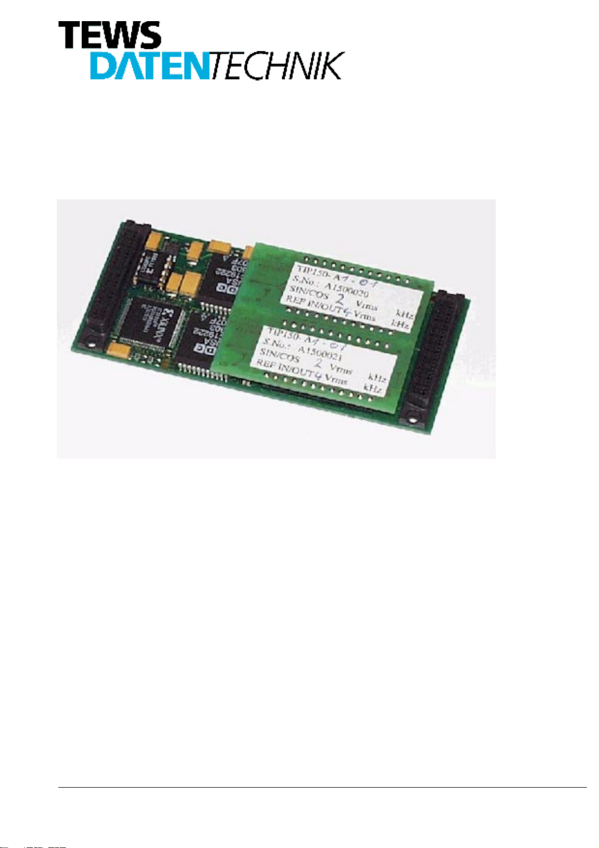
TEWS DATENTECHNIK TIP150 User manual

TIP150
1 or 2 Channel
Synchro/Resolver-To-Digital-Converter
Version 1.1 Revision A
User Manual
Issue 1.1
19 December 1996
D75150801
TEWS DATEN
TECHNIK
GmbH
Am Bahnhof 7
D-25469 Halstenbek
Germany
Tel.: +49 (0)4101 4058-0
Fax.: +49 (0)4101 4058-19
7,3 8VHU 0DQXDO 9HUVLRQ

7,3 8VHU 0DQXDO 9HUVLRQ
TIP150-30
One Channel Tracking RDC,
Converter Accuracy 4 arcmin + 1 LSB
TIP150-31
One Channel Tracking RDC,
Converter Accuracy 2 arcmin + 1 LSB
TIP150-40
Two Channel Tracking RDC,
Converter Accuracy 4 arcmin + 1 LSB
TIP150-41
Two Channel Tracking RDC,
Converter Accuracy 2 arcmin + 1 LSB
Signal Conditioning Adapter
TIP150-A1-xx Resolver
TIP150-A2-xx Resolver with
Reference Oscillator
TIP150-A3-xx High Precision
Syncro / Resolver
TIP150-A4-xx High Precision
Syncro / Resolver
with Refernence Oscillator
This manual covers all products

7,3 8VHU 0DQXDO 9HUVLRQ
This document contains information, which is proprietary to TEWS DATEN
TECHNIK
GmbH. Any reproduction
without written permission is forbidden.
TEWSDATEN
TECHNIK
GmbHhasmadeanyefforttoensure thatthismanualisaccurateandcomplete.Howe-
ver TEWS DATEN
TECHNIK
GmbH reserves the right to change the product described in this document at any
time without notice.
This product has been designed to operate with IndustryPack compatible carriers. Connection to incompatible
hardware is likely to cause serious damage.
TEWS DATEN
TECHNIK
GmbH is not liable for any damage arising out of the application or use of the device
described herein.
Issue Desscription Date
1.0 First Issue 13. Sep. 1995
1.1 Hardware Version 1.1 REV. A 19. Dec.
1996
K1995 / 96 by TEWS DATEN
TECHNIK
GmbH
IndustryPack is a registered trademark of GreenSpring Computers, Inc

7,3 8VHU 0DQXDO 9HUVLRQ
1. Product Description 6...............................
2. Technical Specification 7............................
3. Functional Description 8.............................
3.1. Tracking Rate Characteristics 8...............................
3.2. Automatically Resolution Change 9...........................
4. ID Prom Contents 10..................................
4.1. ID PROM Contents TIP150-XX V1.1 10........................
4.2. ID PROM Contents TIP150 Model Dependent 10................
5. IP Addressing 11.....................................
5.1. Channel 1 Data Register Address $00 11........................
5.2. Channel 1 Status Register Address $03 12.....................
5.2.1. BUILT-IN-TEST 12.........................................
5.2.2. LOSS-OF-SIGNAL 12......................................
5.3. Channel 1 Control Register Address $05 13....................
5.3.1. Resolution Select 13........................................
5.3.2. Enable Synchronous Status Latch 14..........................
5.3.3. Enable Synchronous Conversion 14...........................
5.4. Channel 2 Data Register Address $08 15........................
5.5. Channel 2 Status Register Address $0B 15.....................
5.5.1. BUILT-IN-TEST 15.........................................
5.5.2. LOSS-OF-SIGNAL 16......................................
5.6. Channel 2 Control Register Address $0D 16....................
5.6.1. Resolution Select 17........................................
5.6.2. Enable Synchronous Status Latch 17..........................
6. Operating Modes 18..................................
6.1. Operating With Synchronous Status Latch 18....................
6.2. Operating With Synchronous Conversion 18....................
7. Signal Conditioning Adapter 19........................
7.1. Adapter Connections 19.....................................
7.1.1. 20 Pin Adapter Connector 19.................................
8. Installation Hints 21..................................
9. I/O Pin Assignment 21.................................
9.1. 50 pin IP I/O connector 21.....................................

7,3 8VHU 0DQXDO 9HUVLRQ
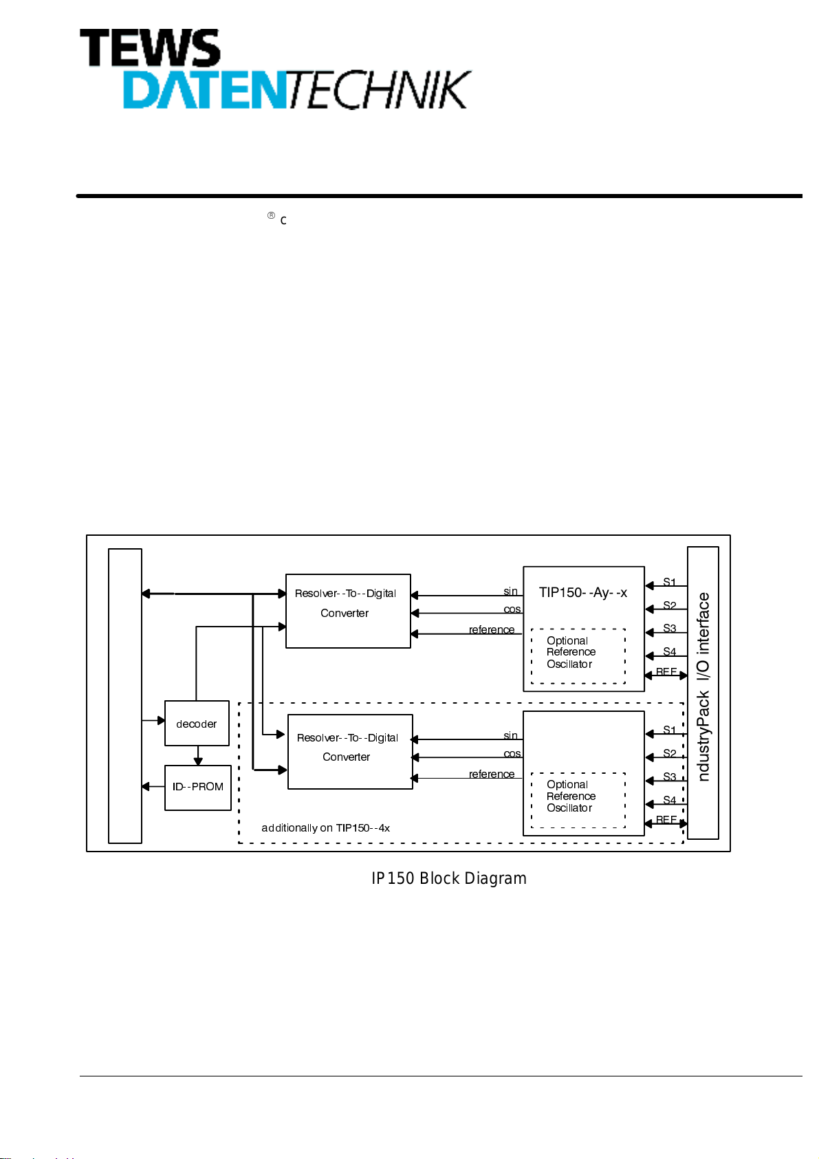
Figure 1: TIP150 Block Diagram 6.................................
Figure 2: Tracking Rate Characteristics for Converter Options 8.......
Figure 3: ID PROM Contents TIP150-XX V1.0 10.....................
Figure 4: ID PROM Contents Model Dependent 10...................
Figure 5: DATA_RDC1 Channel 1 Data Register 11...................
Figure 6: STATUS_RDC1 Channel 1 Status Register 12...............
Figure 7: CONTR_RDC1 Channel 1 Control Register 13...............
Figure 8: Resolution Select Bits 13.................................
Figure 9: DATA_RDC2 Channel 2 Data Register 15...................
Figure 10: STATUS_RDC2 Channel 2 Status Register 15..............
Figure 11: CONTR_RDC2 Channel 2 Control Register 16..............
Figure 12: Resolution Select Bits 17................................
Figure 13:TIP150 Adapter Board Placement 19......................
Figure 14: Adapter Board Connector 20.............................
7,3 8VHU 0DQXDO 9HUVLRQ
1. Product Description
The TIP150 is an IndustryPack
9
compatible module with one channel ( TIP150-3x ) or two channel
(TIP150-4x )of a Tracking Resolver-To-DigitalConverter (RDC). It iswellsuitedfor both, SynchroandResolver
applications.
The TIP150 is designed for use in high performance commercial systems. It can by used for many applications
likemotorcontrol,robotaxiscontrol, processcontrol,radarantennapositioninformation,andCNCmachinetoo-
ling.
The TIP150 utilizes up to two versatile state-of-the-art Synchro or Resolver-To-Digital Converters featuring pro-
grammable resolution. Resolution programming allows selection of either 10-, 12-, 14-, 16-bit conversion, this
combines the high tracking rate of a10-bit converter with the precision of a16-bit converter.
The TIP150 is available with a converter accuracy of 4 arcmin + 1 LSB ( TIP150-x0 ) or 2 arcmin + 1LSB
( TIP150-x1 ).
The velocity output from the TIP150, which can be used to replace a tachometer, is a 4V signal with a linearity
of 0.75% of output voltage.
Signal Conditioning Adapters (TIP150-Ay-xx) are required for each Synchro / Resolver channel to configure
Converter Input levels for Synchros, Resolvers and optional Reference input/output by passive components.
Theoptionalreferenceoscillatoronboardof theSignal ConditioningAdapterprovidefactoryselectablefrequen-
cies from 2KHz to 20KHz. For highest accuracy the reference oscillator compensates automatically the phase
error generated by the Resolver or Synchro.
,QGXVWU\3DFN ORJLF LQWHUIDFH
5HVROYHU 7R 'LJLWDO
,' 3520
GHFRGHU
,QGXVWU\3DFN O2 LQWHUIDFH
&RQYHUWHU
VLQ
FRV
5HIHUHQFH
2VFLOODWRU
5HVROYHU 7R 'LJLWDO
&RQYHUWHU
DGGLWLRQDOO\ RQ 7,3 [
6
6
6
6
5()
6
6
6
6
5()
UHIHUHQFH 2SWLRQDO
7,3 $\ [[
VLQ
FRV
5HIHUHQFH
2VFLOODWRU
UHIHUHQFH 2SWLRQDO
7,3 $\ [[
Figure 1: TIP150 Block Diagram

7,3 8VHU 0DQXDO 9HUVLRQ
2. Technical Specification
TIP150-xx
Logic Interface IndustryPack9Logic Interface
Size single wide IP
I/O Interface 50-conductor flat cable
Wait States IDSEL 0waitstate
IOSEL to control registers 0 wait state
IOSEL to data register 2 wait states
Accuracy of RDC 4 arcmin + 1LSB for TIP150-x0
2 arcmin + 1LSB for TIP150-x1
Power Requirements 100 mA @ +5V
15 mA @ +12V, no load
35 mA @ -12V, no load
Temperature Range Operating 0ECto 70EC
Storage -25EC to 125EC
Humidity 5 - 95% non-condensing
TIP150-A1-xx
Input Voltage Configured by resistors ( 0.1% accuracy )
Input Frequency DC to 40 KHz
TIP150-A2-xx
Input Voltage Configured by resistors ( 0.1% accuracy )
Input Frequency 2 KHzto 20KHz,dependant of configuration of on boardrefer-
ence oscillator
Reference Oscillator 2KHz to 20 KHz, max. 11.8V rms 70 mA
configured on Signal Conditioning Adapter by resistors
TIP150-A3-xx
Input Voltage 11.8 V rms or 90.0V rms, configured by high precision match-
ing resistor array
Input Frequency DC to 40 KHz
TIP150-A4-xx
Input Voltage 11.8 V rms or 90.0V rms, configured by high precision match-
ing resistor array
Input Frequency 2 KHzto 20KHz,dependant of configuration of on boardrefer-
ence oscillator
Reference Oscillator 2KHz to 20 KHz, max. 11.8V rms 70 mA
configured on Signal Conditioning Adapter by resistors

7,3 8VHU 0DQXDO 9HUVLRQ
3. Functional Description
The TIP150 provides one or two channel of Resolver-To-Digital Converter. Theinput signals are conditioned by
Signal Conditioning Adapters (TIP150-Ay-xx) on the TIP150. A Signal Conditioning Adapter is required for each
channel of the TIP150. Four types of Signal Conditioning Adapters are available:
TIP150-A1-xx Resolver Signal Conditioning Adapter.
TIP150-A2-xx Resolver Signal Conditioning Adapter with reference oscillator.
TIP150-A3-xx High precision Synchro/Resolver Signal Conditioning Adapter.
TIP150-A4-xx High precision Synchro/Resolver Signal Conditioning Adapter with reference oscillator.
The output voltage of the optional reference oscillator placed on the TIP150-A2/A4-xx is max. 11.8V rms with
70mA output current.
The TIP150 module supports the mode of synchronous status and data latch. If the module is a TIP150-4X with
two RDC on board it support the mode of synchronous status and data latch for each channel or synchronous
data and status latch for both channels simultaneous.
3.1. Tracking Rate Characteristics
Tracking Rate, Bandwidth and Velocity Scaling is dependent on the Resolution of the RDC and the Reference
Oscillator Frequency. RPS (rotation per second)
5HVROXWLRQ
%LW %LW %LW %LW
Reference
Frequency
2KHz
5KHz
10 KHz
20 KHz
8QLW
%DQGZLGWK +]
7UDFNLQJ 5DWH 536
Velocity Voltage
Scaling RPS/Volts
285.4
1116.1
0.0036
285.4
1116.1
0.0036
285.4
1116.1
0.0036
285.4
1116.1
0.0036
285.4
279.0
0.00143
285.4
279.0
0.00143
285.4
279.0
0.00143
349.5
279.0
0.00143
285.4
69.8
0.0573
285.4
69.8
0.0573
285.4
69.8
0.0573
110.5
17.4
0.2294
90.2
17.4
0.2294
90.2
17.4
0.2294
%DQGZLGWK +]
7UDFNLQJ 5DWH 536
Velocity Voltage
Scaling RPS/Volts
%DQGZLGWK +]
7UDFNLQJ 5DWH 536
Velocity Voltage
Scaling RPS/Volts
%DQGZLGWK +]
7UDFNLQJ 5DWH 536
Velocity Voltage
Scaling RPS/Volts
Figure 2: Tracking Rate Characteristics for Converter Options

7,3 8VHU 0DQXDO 9HUVLRQ
3.2. Automatically Resolution Change
If the Build-In-Test bits of the converter indicate an error the resolution bitsRES0 and RES1 of the Channel Con-
trol register whichnormally control the resolution will beignored andthe resolution is changedfrom it’sprogram-
med value one step down to a lower resolution. This allows the converter to settle out faster. After the converter
has settled out the resolution is switched back to the programmed resolution.
For example: If 12 bit resolution is programmed and Build-In-Test indicates an error the resolution
changes to 10 bit until the converter settled out.
If 14 bit resolution is programmed and Build-In-Test indicates an error the resolution
changes to 12 bit until the converter settled out.
If 16 bit resolution is programmed and Build-In-Test indicates an error the resolution
changes to 14 bit until the converter settled out.

7,3 8VHU 0DQXDO 9HUVLRQ
4. ID Prom Contents
4.1. ID PROM Contents TIP150-XX V1.1
ADDRESS FUNCTION
$ 01 ASCII ’I’ $ 49
$ 03 ASCII ’P’ $ 50
$ 05 ASCII ’A’ $ 41
$07 ASCII’C’ $43
$ 09 Manufacturer ID $ B3
$ 0B Model Number $ 14
$ 0D Revision $ 11
$ 0F RESERVED $ 00
$ 11 Driver-ID low-byte $ 00
$ 13 Driver-ID high-byte $ 00
$ 15 number of bytes used $ 0D
$17 CRC $seeFigure4
$ 19 Version -XX $ see Figure 4
$1B $00
...... Not used .......
$3F $00
Figure 3: ID PROM Contents TIP150-XX V1.0
4.2. ID PROM Contents TIP150 Model Dependent
TIP150 C R C $17 Version $19
-30 DA 1E
-31 FB 1F
-40 4F 28
-41 6E 29
Figure 4: ID PROM Contents Model Dependent

7,3 8VHU 0DQXDO 9HUVLRQ
5. IP Addressing
The TIP150 is controlled by a set of registers, which is directly accessible in the I/O address space of the IP.
The control registers are automatically cleared by assertion of IP_RESET.
ADDRESS NAME FUNCTION SIZE ACCESS
$ 00 DATA_RDC1 Channel 1 Data Register word R
$ 03 STATUS_RDC1 Channel 1 Status Register byte R
$ 05 CONTR_RDC1 Channel 1 Control Register byte R/W
$ 06 reserved word -
Only for TIP150-4X
$ 08 DATA_RDC2 Channel 2 Data Register word R
$ 0B STATUS_RDC2 Channel 2 Status Register byte R
$ 0D CONTR_RDC2 Channel 2 Control Register byte R/W
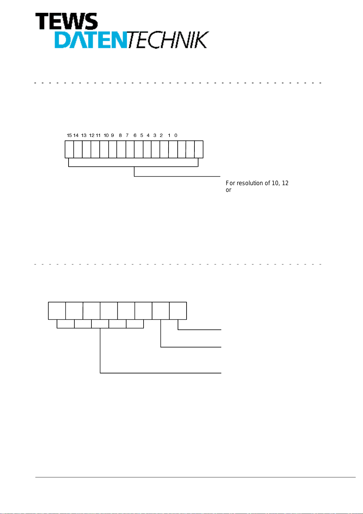
5.1. Channel 1 Data Register Address $00
TheChannel1DataRegistercontainstheconverteddatavalueofthe ResolverorSynchro. Whentheresolution
isset toless than16bits, allunusedbitsarereadas’0’.Theconversionresultis alwaysMSBaligned.Theresolu-
tion is controlled by the Channel 1 Control Register.
Ifthe Build-In-TestbitoftheChannel1StatusRegisterisreadas’1’theresolutionchangedfrom it’sprogrammed
value one step down to a lower resolution. This allows the converter to settle out faster.
%LW 5'& YDOXH
For resolution of 10, 12
or 14 bits unused data
bits are read as ’0’
Figure 5: DATA_RDC1 Channel 1 Data Register
For example: If 12 bit resolution is programmed: Data Register = $XXX0
If 16 bit resolution is programmed: Data Register = $XXXX

7,3 8VHU 0DQXDO 9HUVLRQ
5.2. Channel 1 Status Register Address $03
TheSTATUS_RDC1Register isabytewidereadregisterandindicatesthedataconversionstatusof theconver-
ter channel 1.
%8,/7 ,1 7(67
/266 2) 6,*1$/
DOOZD\V UHDG DV ]HUR
BIT
LOS
Figure 6: STATUS_RDC1 Channel 1 Status Register
5.2.1. BUILT-IN-TEST
Bit0 Built-In-Test(BIT) indicatesanerror.Ifthedifferencebetweeninputandoutputangelsexceedsapproxima-
tely 55 LSBs (of the selected resolution) the BIT bit is read as ’1’. This condition will occur during a large step
and reset after the converter settles out.
If the Build-In-Test bit of the Status Register is read as ’1’ the resolution changed from it’s programmed value
one step down to a lower resolution. This allows the converter to settle out faster.
This bit will change to ’1’ for an overvelocity condition, because the converter loop cannot maintain input-output
or/ and if the converter malfunctions where it cannot maintain the loop at a null.
Bit0willalsoreadas’1’ifboth,sinandcos inputvoltages areless than800mVpeakorifthedifferentialreference
voltages is less than 20mV peak.
5.2.2. LOSS-OF-SIGNAL
ThisstatusbitonlyexistsforTIP150moduleswithSignalConditioningAdapters witchhaveareferenceoscillator
on board ( TIP150-A2-xx or TIP150-A4-xx ). For all other Signal Conditioning Adapters this bit always read as
’0’.
ReadingBit1Loss-of-Signal(LOS)as’1’indicatesthatbothsinandcosinputoftheonboardreferenceoscillator
are less than 800mV peak.

7,3 8VHU 0DQXDO 9HUVLRQ
5.3. Channel 1 Control Register Address $05
The Channel 1 Control Register CONTR_RDC1 is a byte wide read/write register.
DOOZD\V UHDG DV ]HUR D ZULWH DFFHVV
(6/
5HVROXWLRQ 6HOHFW
(6&
5(6 5(6
(QDEOH 6\QFKURQRXV 6WDWXV /DWFK
Enable Synchronous Conversion Channel 1
and Channel 2 ( TIP150-4x only )
GRQW FDUH
WR WKHVH ELWV KDV QR HIIHFW
;;
Figure 7: CONTR_RDC1 Channel 1 Control Register
5.3.1. Resolution Select
Bit 0 and bit 1 of the Channel1 Control Register are used to program the resolution of the converter.
5(6 5(6 5(62/87,21
00
01
10
11
10 bits
12 bits
14 bits
16 bits
Figure 8: Resolution Select Bits

7,3 8VHU 0DQXDO 9HUVLRQ
5.3.2. Enable Synchronous Status Latch
If bit 2 of the Channel 1 Control Register is set to ’1’ the Channel 1 Status Register will be latched at the time
reading the Channel 1 Data Register, ensuring that the Channel 1 Status Register reflectsthe stateat data read
time. The status will remain latched until it is read.
To use this mode of operation, bit 3 of the Channel 1 Control Register must be set to ’0’.
5.3.3. Enable Synchronous Conversion
If bit 3 is set to ’1’ the Synchronous Conversion of Channel 1 and Channel 2 is enabled.
A readaccess to the Channel 1 DataRegister starts the conversion for channel 1 and2, latches the Status Regi-
ster for channel1and2andprovides thedatafor channel1. LatchingtheStatusRegisterensuresthattheStatus
Registers reflect the state at data read time. The status of both Status Registers will remain latched until aread
access to Channel 2 Status Register.
This bitisonlyactivefor TIP150-4Xwith two channelresolver-to-digitalconverter. For TIP150-3X thisbit is don’t
care.
1RWH
$IWHU 5HVHW DOO ELWV DUH VHW WR GHIDXOW FRQGLWLRQV DUH ELW FRQYHU
VLRQ QR V\QFKURQRXV FRQYHUVLRQ
7,3 8VHU 0DQXDO 9HUVLRQ
5.4. Channel 2 Data Register Address $08
The Channel2DataRegister contains theconverted data valueof theSynchroor Resolver.When theresolution
isset toless than16bits, allunusedbitsarereadas’0’.Theconversionresultis alwaysMSBaligned.Theresolu-
tion is controlled by the Channel 2 Control Register.
Ifthe Build-In-TestbitoftheChannel2StatusRegisterisreadas’1’theresolutionchangedfrom it’sprogrammed
value one step down to a lower resolution. This allows the converter to settle out faster.
%LW 5'& YDOXH
For resolution of 10, 12
or 14 bits unused data
bits are read as ’0’
Figure 9: DATA_RDC2 Channel 2 Data Register
For example: If 12 bit resolution is programmed: Data Register = $XXX0
If 16 bit resolution is programmed: Data Register = $XXXX
5.5. Channel 2 Status Register Address $0B
TheSTATUS_RDC2Register isabytewidereadregisterandindicatesthedataconversionstatusof theconver-
ter channel 2.
%8,/7 ,1 7(67
/266 2) 6,*1$/
DOOZD\V UHDG DV ]HUR
BIT
LOS
RQO\ IRU 7,3 ; ZLWK
7,3 $ [[ RU 7,3 $ [[
Figure 10: STATUS_RDC2 Channel 2 Status Register
5.5.1. BUILT-IN-TEST
Bit0 Built-In-Test(BIT) indicatesanerror.Ifthedifferencebetweeninputandoutputangelsexceedsapproxima-
tely 55 LSBs (of the selected resolution) the BIT bit is read as ’1’. This condition will occur during a large step
and reset after the converter settles out.
Ifthe Build-In-TestbitoftheChannel2StatusRegisterisreadas’1’theresolutionchangedfrom it’sprogrammed
value one step down to a lower resolution. This allows the converter to settle out faster.

7,3 8VHU 0DQXDO 9HUVLRQ
This bit will change to ’1’ for an overvelocity condition, because the converter loop cannot maintain input-output
or / and if the converter malfunctions where it cannot maintain the loop at a null.
Bit0willalsoreadas’1’ifboth,sinandcos inputvoltages areless than800mVpeakorifthedifferentialreference
voltages is less than 20mV peak.
5.5.2. LOSS-OF-SIGNAL
ThisstatusbitonlyexistsforTIP150moduleswithSignalConditioningAdapters witchhaveareferenceoscillator
on board ( TIP150-A2-xx or TIP150-A4-xx ). For all other Signal Conditioning Adapters this bit always read as
’0’.
ReadingBit1Loss-of-Signal(LOS)as’1’indicatesthatbothsinandcosinputoftheonboardreferenceoscillator
are less than 800mV peak.
5.6. Channel 2 Control Register Address $0D
The Channel 2 Control Register CONTR_RDC2 is a byte wide read/write register.
DOOZD\V UHDG DV ]HUR D ZULWH DFFHVV
(6/
5HVROXWLRQ 6HOHFW
;
5(6 5(6
(QDEOH 6\QFKURQRXV 6WDWXV /DWFK
WR WKHVH ELWV KDV QR HIIHFW
'RQW FDUH
;;
Figure 11: CONTR_RDC2 Channel 2 Control Register

7,3 8VHU 0DQXDO 9HUVLRQ
5.6.1. Resolution Select
Bit 0 and bit 1 of the Channel 2 Control Register are used to program the resolution of the converter.
5(6 5(6 5(62/87,21
00
01
10
11
10 bits
12 bits
14 bits
16 bits
Figure 12: Resolution Select Bits
5.6.2. Enable Synchronous Status Latch
If bit 2 of the Channel 2 Control Register is set to ’1’ the Status Register will be latched at the time reading the
Channel 2 Data Register, ensuring that the status register reflects the state at data read time. The status will
remain latched until it is read.
To use this mode of operation, bit3 of the Channel 1 Control Register must be set to ’0’.
1RWH
$IWHU 5HVHW DOO ELWV DUH VHW WR WKHUHIRUH GHIDXOW FRQGLWLRQV DUH ELW
FRQYHUVLRQ LQGHSHQGHQW RSHUDWLRQ

7,3 8VHU 0DQXDO 9HUVLRQ
6. Operating Modes
If bit2 and bit3 (only for TIP150-4X) of the Control Register(s) are set to ’0’ the Status Register(s) reflects the
actual conditions of the converter. It is meaningful to use a mode which latches the Status of the data reading.
6.1. Operating With Synchronous Status Latch
Operatingwithsynchronous statuslatchfor eachchannelseparatelyisselectedif bit2oftherespectiveChannel
Control Register is set to’1’. In this case the Channel Status Register latches the status at Data Register read
time. The latch is released by a read access to the Status Register.
Sequence : read Data freeze the Status at Data read
read Status release status latch
check Build-In-Test (bit0) If bit0 is read as ’0’,the data value is valid.
1RWH
7R XVH WKLV PRGH ELW RI WKH &KDQQHO &RQWURO 5HJLVWHU PXVW EH VHW WR
IRU D PRGXOH ZLWK WZR 6\QFKUR5HVROYHU WR GLJLWDO FRQYHUWHU RQ
ERDUG
6.2. Operating With Synchronous Conversion
Only usable with two Synchro/Resolver-to-digital converter on board (TIP150-4X).
Operatingwithsynchronous ConversionforChannel1andChannel2 isselectedifbit3oftheChannel1Control
Registers(CONTR_RDC1)is setto’1’.Inthiscasethevalueofchannel2isconvertedsimultaneously withchan-
nel 1and both StatusRegisters arelatched at Data Register readtime. Torelease the latches of the Status Regi-
sters of channel 1 and channel 2 the user must read the Status Register of Channel 2 (STATUS_RDC2).
Sequence : read Data Channel 1 start conversion for channel 1 and 2
latch the status for channel 1 and 2
read data for channel 1
read Status Channel 1
read Data Channel 2 release Data Channel 2
read Status Channel 2 release latch of Channel 1 and Channel 2
Status Register
check Build-In-Test (bit0) If bit0 is read as ’0’, the data value is valid.
of both Status Registers

7,3 8VHU 0DQXDO 9HUVLRQ
7. Signal Conditioning Adapter
For the TIP150 the concept of Signal Conditioning Adapters is used. This makes it very easy to use the various
types of Resolvers and Synchros. Four different kinds of Signal Conditioning Adapters exist:
TIP150-A1-xx Resolver Signal Conditioning Adapter.
TIP150-A2-xx Resolver Signal Conditioning Adapter with
reference oscillator.
TIP150-A3-xx High precision Synchro/Resolver Signal Conditioning
Adapter.
TIP150-A4-xx High precision Synchro/Resolver Signal Conditioning
Adapter with reference oscillator.
The Converter inputs and optional Reference input/output are factory configured by resistors or resistor arrays
on the Signal Conditioning Adapters. Each version of the four different kinds of Signal Conditioning Adapter
gets its own ordering number from the factory ( replaces the -xx ). The -xx specify the signal voltage,reference
voltage and if the adapter is an A2/A4 the reference frequency.
7.1. Adapter Connections
The Signal Conditioning Adapters TIP150-Ay-xx are usedto link the IP-I/O connector of the TIP150-XX module
to the resolver-to-digital converter.
,3 /RJLF ,QWHUIDFH
,2 ,QWHUIDFH
Signal Conditioning Adapter
for Channel 1
7,3 $\ [[
7,3 $\ [[
Signal Conditioning Adapter
for Channel 2
( TIP150-4x only )
Figure 13:TIP150 Adapter Board Placement
7.1.1. 20 Pin Adapter Connector
Function and Pin-Number are valid for Adapter Boards for Channel 1 and Channel 2.
Table of contents
Popular Media Converter manuals by other brands


Sonifex
Sonifex Redbox RB-ADDA2 User handbook

Antrica
Antrica ANT-1773 quick start guide

midiplus
midiplus STUDIO 2 Quick start manual

Connection
Connection SLI 2.2 owner's manual
 user manual")
Lynx Studio Technology
Lynx Studio Technology Aurora(N) user manual

Intellisystem
Intellisystem IT-SDS-3016-T-16D Series user manual