manuals.online logo
Brands
  1. Home
  2. •
  3. Brands
  4. •
  5. Texas Instruments
  6. •
  7. Motherboard
  8. •
  9. Texas Instruments ADS1610EVM User manual

Texas Instruments ADS1610EVM User manual

User's GuideSLAU180A – May 2006 – Revised August 2006
ADS1610EVM
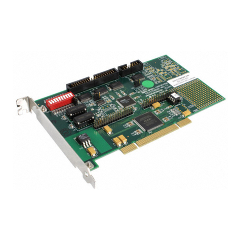
This user’s guide describes the characteristics, operation, and use of the ADS161016-bit, 10-MSPS high-speed, parallel interface, analog-to-digital converter evaluationboard. A complete circuit description, a schematic diagram, and a bill of materials isincluded. Contact the Product Information Center or e-mail [email protected]for questions regarding this EVM.
Contents1 EVM Overview ...................................................................................... 22 Introduction .......................................................................................... 23 Digital Interface ..................................................................................... 44 Power Supplies ..................................................................................... 85 Using the EVM ...................................................................................... 86 Related Documentation from Texas Instruments ............................................. 13Appendix A Bill of Materials .......................................................................... 14Appendix B Layout and Schematic .................................................................. 17
List of Figures
1 Input Circuitry ....................................................................................... 32 TSW1100 and ADS1610EVM Setup ............................................................. 83 TSW1100 Screen Shot ............................................................................ 94 Test Results With a 100-kHz Input Frequency ................................................ 105 Test Results With a 250-kHz Input ............................................................. 106 Test Results With a 500-kHz Input ............................................................. 117 Test Results With a 1-MHz Input ............................................................... 118 Test Results With a 2-MHz Input ............................................................... 12B-1 Top Layer – Layer 1 .............................................................................. 17B-2 Split Ground Plane – Layer 2 .................................................................... 17B-3 Split Power Plane – Layer 3 ..................................................................... 18B-4 Split Power Plane – Layer 4 ..................................................................... 18B-5 Split Ground Plane – Layer 5 .................................................................... 19B-6 Bottom Layer – Layer 6 .......................................................................... 19
List of Tables
1 Reference Voltages ................................................................................ 32 Jumper Setting ...................................................................................... 43 Switch Function Control, SW1 .................................................................... 44 Digital Jumper ....................................................................................... 55 Memory Space Address ........................................................................... 66 Assignment and Function at J18 ................................................................. 67 Assignment and Function at J2 ................................................................... 78 Assignment and Function at J10/P10 ............................................................ 7
SLAU180A – May 2006 – Revised August 2006 ADS1610EVM 1Submit Documentation Feedback
www.ti.com
1 EVM Overview
1.1 Features
2 Introduction
2.1 Analog Interface
2.1.1 Analog Input Signal Conditioning
EVM Overview
•Full-featured evaluation board for the ADS1610 10-MSPS high-speed 16-bit, single-channel, parallelinterface, delta sigma type analog-to-digital converter.•Onboard signal conditioning•Onboard reference, with recommended buffer circuitry•Input and output digital buffers•Basic system-level logic decoding.
The ADS1610 is high-speed, high-resolution delta sigma ( ∆ Σ ) analog-to-digital converter. It features a datarate of 10 MSPS and an advanced multistage analog modulator combined with an on-chip digitaldecimation filter. The ADS1610 achieves 86 dBFS signal-to-noise ratio (SNR) in a 5-MHz signalbandwidth. The device offers outstanding performance at these speeds with a total harmonic distortion of–94 dB. The ADS1610 ∆ Σ topology provides key system-level design advantages with respect to antialiasfiltering and clock jitter. The design of the antialias filter is simplified because the on-chip digital filtergreatly attenuates out-of-band signals. The ADS1601 filter has a brick wall response with a flat pass band(±0.0002 dB of ripple) followed immediately by a wide stop band (5 MHz to 55 MHz). Clock jitter becomesespecially critical when digitizing high-frequency, large-amplitude signals. The ADS1610 significantlyreduces clock jitter sensitivity by an effective averaging of clock jitter as a result of oversampling the inputsignal. Output data is supplied over a parallel interface and easily connects to TMS320 digital signalprocessors (DSP). The power dissipation can be adjusted with an external resistor, allowing for reductionat lower operating speeds. With its outstanding high-speed performance, the ADS1610 is well-suited fordemanding applications in data acquisition, scientific instruments, test and measurement equipment, andcommunications.
The ADS1610EVM is a stand-alone, full-featured system that offers data-sheet performance. Additionally,the EVM conforms to a common electrical and mechanical pinout for digital I/O enabling it to be quicklyadapted to various host platforms.
The analog interface consists of the following subsections:1. Analog input2. External reference generation3. Modulator clock
The ADS1610 measures the differential signal, VIN = (AINP-AINP), against the differential reference,VREF = (VREFP – VREFN). The analog input signal can be applied to the board through the SMAconnectors J4 and J41. The board arrives with the input circuitry configured for single-ended in, differentialoutput, as shown in Figure 1 . It has a 50 - Ωtermination; therefore, the signal source needs to be able toprovide a 3 -V single-ended signal with this termination. The single-ended analog signal can be applied atJ4.
The onboard input driver is designed using the wide-band, low-distortion, fully differential amplifier(THS4503) from Texas Instruments. The amplifier is configured for a gain of 2. The THS4503 can directlyaccept differential signals or be used to convert a single-ended input signal to a differential one. Thefactory-set condition is for a single-ended input converted to fully differential at the output of the THS4503.The desired output common-mode signal is fed through pin 2 of the THS4503. The required commonmode is 2.5 V. This voltage is generated onboard in the reference voltage generation circuitry.
2ADS1610EVM SLAU180A – May 2006 – Revised August 2006Submit Documentation Feedback
www.ti.com
Vin
THS4503
AINP
AINN
47 pF
787 W
+VCC
0.1 Fm
10 Fm
10 Fm
0.1 Fm
12 W
100 pF
12 W100 pF
100 pF
787 W
-VCC
374 W
402 W
56.2 W
Vocm
+2.5 V
47 pF
2.1.2 External Reference Generation
IntroductionThe ADS1610 has relaxed antialiasing filter requirements because it is a delta sigma converter. A simpleantialiasing filter comprising a 24- Ωresistor and a 300- pF capacitor with a –3-dB bandwidth of 22 MHz isused at the output of the THS4503.
Figure 1. Input Circuitry
The ADS1610 operates from an external voltage reference. The reference voltage VREF is set by thedifferential voltage between VREFN and VREFP: VREF = (VREFP-VREFN). VMID must be 2.5 V.
The ADS1610EVM has onboard reference generation circuitry using the low-noise, high-speed THS4031from Texas Instruments. Three of these amplifiers are used to generate the REFP (VREFP), CML (VMID)and REFM (VREFM) voltages. The CML voltage generated in this circuitry also is used as thecommon-mode voltage for the input driver (THS4503). The three reference voltages can be adjusted usingthe trim potentiometers R37, R38, and R40.
The reference voltage source for the onboard reference generation circuitry is selectable. If W1 jumperposition is across pins 1 and 2, then AVDD1 is selected. When the jumper is placed across pins 2 and 3,the REF02 is selected as the source. The ADS1610EVM leaves the factory with a short across pins 2 and3 of W1.
The factory-set voltages are 4 V, 2.5 V, and 1 V for VREFP, VCML, and VREFM, respectively. Thesevoltages provide a reference voltage of 3 V single-ended. The ADS1610 with a 3-V reference can achievean SNR of 86 dBFS in the 0 – 5-MHz bandwidth.
If the application requires a smaller reference voltage, then potentiometers R37 and R38 can be adjustedto generate the desired voltage. Be aware that there is a tradeoff between SNR and reference voltages.Table 1 gives the reference voltage versus SNR tradeoff.
Table 1. Reference Voltages
Reference VREFM VCML VREFP Peak In-Band SNR
3 V 1 2.5 4 86
2.5 V 1.25 2.5 3.75 85
2 V 1.5 2.5 3.5 83
SLAU180A – May 2006 – Revised August 2006 ADS1610EVM 3Submit Documentation Feedback
www.ti.com
2.1.3 Clock Source
3 Digital Interface
3.1 Board-Level Control
3.1.1 DIP Switch Options
Digital Interface
For more information on the reference generation circuitry, see sheet 6 of the ADS1610EVM schematic, atthe end of this user’s guide.
The ADS1610 uses the external clock signal applied to the CLK input pin as the modulator clock. Inputsampling is controlled by this clock signal. As with any high-speed data converter, a high-quality clock isessential for achieving optimum performance. In order to maximize SNR performance of the converter,keep the jitter on this clock source below those recommended in the ADS1610 data sheet.
The modulator clock can be fed into the ADS1610 from two sources. It can be applied via SMA connector(J4) or from the onboard source. The onboard source is the 60-MHz oscillator installed at X1. Thefactory-set condition applies the onboard 60-MHz oscillator to the CLK pin of the ADS1610. Theuser-supplied external clock must be fed to the board through the SMA connector, J4. The board has afootprint at R9 for a 50 - Ωtermination on this line. It can be installed at the user’s discretion. If R9 is notinstalled by the user and the user clock is generated from a 50- Ωsource, then be sure to reduce the clockamplitude to half.
To switch from the onboard oscillator to the user clock applied at J4, change the position of jumper of W3from pins 1–2 to 2–3.
The performance of the ADS1610 is sensitive to clock jitter; see the data sheet for the requirements.
Table 2. Jumper Setting
Reference 1-2 2-3 DescriptionDesignator
W1 Installed
(1)
Not installed Set voltage on AVDD1 as source for the reference generation circuitry.Not installed Installed Set voltage REF02 as the source for the reference generation circuitry.W2 Installed
(1)
Not installed Enable 60-MHz oscillatorNot installed Installed Disable 60-MHz oscillatorW3 Installed
(1)
Not installed Set modulator clock to onboard 60-MHz oscillatorNot installed Installed Set modulator clock to user-supplied clock via J4.
(1)
Factory installed
This section describes the digital sections and pinout of the ADS1610EVM.
Optional settings for the ADS1610 are set and controlled manually via a DIP switch – SW1. The functionscontrolled by this switch are summarized in Table 3 .
Table 3. Switch Function Control, SW1
Switch, SW1
Position Function ON(LO) OFF(HI)
1 Mode 0 pin Set M0 to 0 Set M0 to 12 Mode 1 pin Set M1 to 0 Set M0 to 13 Power-down bit Device is powered down Device is not powered down4 Not used5 Not used6 Not used
4ADS1610EVM SLAU180A – May 2006 – Revised August 2006Submit Documentation Feedback
www.ti.com
3.1.2 Jumper Options
3.1.3 ADS1610EVM OTR LED
3.1.4 ADS1610 Reset
3.1.5 Interrupt Source
3.1.6 Base Address and Chip Select
Digital Interface
Table 3. Switch Function Control, SW1 (continued)
Switch, SW1
Position Function ON(LO) OFF(HI)
7 Not used8 Not used
Four jumpers are associated with the digital control section; their functions are detailed in Table 4 .
Table 4. Digital Jumper
Reference 1-2 2-3 DescriptionDesignator
W20 Installed Not installed Set SYNCB to output of combinatory logicNot installed Installed
(1)
Set SYNCB to user reset switchW23 Installed
(1)
Not installed Set DRDY_OUT to DRDY of ADS1610Not installed Installed Set DRDY_OUT to inverted DRDY of ADS1610.J19 2-1 Installed
(1)
N/A Set U16A pin 2 to LOW. Used in EVM address decoding logic.J19 3-4 Installed
(1)
N/A Set U17A pin 2 to LOW. Used in board address decoding logic.
(1)
Factory installed
When the analog input exceeds the positive full-scale value or goes below negative full-scale value ofVREF, the Out of Range (OTR) signal goes HIGH and remain high while the signal is out-of-range. Whenthis condition occurs, LED1 illuminates. To clear the LED, flip-flop U13 must be reset. Depending on whichposition W20 is set to, the LED can be reset manually via SW2 or through programming by issuing a WRoperation from the host processor. The factory-set condition of W20 is a short across pins 2-3. This allowsthe user to manually reset the LED and reset the ADS1610.
The ADS1610 can be asynchronously reset when the SYNC pin is driven low. In reset, all the digitalcircuits are cleared, the data bus is LOW, and DRDY is HIGH. The ADS1610 can be reset in two ways,using an manual reset via SW1 or by programming from the host system. If W20 pins 1-2 are shorted, theSYNC signal must be generated by the host system. If W20 pins 2-3 are shorted, then the SYNC signal tothe ADS1610 is generated manually by momentarily depressing switch SW2.
Some microprocessors only recognize falling edge interrupts; others only recognize rising edge interrupts.Some can be programmed to recognize either. W23 can be set by the user to select either rising edge orfalling edge. If a jumper is across pins 1 and 2, DRDY is applied to DRDY_OUT pin. If jumper short isacross pins 2 and 3, an inverted version of DRDY is applied to DRDY_OUT pin.
The EVM can be mapped into a memory location by setting a base address. The EVM has four possiblebase addresses. The base address is set by J19. When the logic state of the two external address signalsmatches the logic state set up by the two jumpers on J19 and the access is valid memory access, theEVM generates a CS signal for the ADC. This then can be further qualified as a read cycle or a write( RESET) cycle. An installed jumper is equivalent to logic 0 on the corresponding address line. Anuninstalled jumper is equivalent to logic 1 on the corresponding address line.
SLAU180A – May 2006 – Revised August 2006 ADS1610EVM 5Submit Documentation Feedback

www.ti.com
3.2 External Interface
3.3 Data Connector Pinout
Digital Interface
The TMS320C6713 DSK provides two memory spaces for the daughterboards. The two memory spacesenables (CE2 and CE3) are buffered versions of the DSP outputs and are not generated by decode logicon the DSK. The 5-6K EVM uses CE2 to indicate that the access is valid. The places the daughterboardat an address space beginning at 0xA0000000.
Table 5. Memory Space Address
J19 Address Selected
1-2 3-4
0 0 0xA00000000 1 0xA00000041 0 0xA00000081 1 0xA000000C
The pinout for the ADS1610EVM has been arranged to easily mate with the growing range of interfaceadapters. The interface board that is currently available is the 5-6K Interface Board (see SLAU104 ). Thisboard enables any TMS320C5000 DSP platform or TMS320C6000 DSP platform-based DSK withstandard expansion connectors to connect to the EVM.
The data from the ADC is available at J18 and at J2. J18 is available for interfacing to 5-6K interfaceboard, user breadboard, or ribbon cable. Connector J2 is installed to allow users to connect theADS1610EVM directly to the TSW1100 data capture board (see SLAU164 ) from Texas Instruments. Theapplication section of this user’s guide explains how an ADS1610 can be evaluated using the TSW1100and ADS1610EVM.
The pin assignments and function of each of the pins on J2 and J18 are given in Table 6 and Table 7 .
Table 6. Assignment and Function at J18
Description Signal Connector Pin Connector Pin Description
Buffered data bit 0 (LSB) D0 J18.1 J18.2 GroundBuffered data bit 1 D1 J18.3 J18.4 GroundBuffered data bit 2 D2 J18.5 J18.6 GroundBuffered data bit 3 D3 J18.7 J18.8 GroundBuffered data bit 4 D4 J18.9 J18.10 GroundBuffered data bit 5 D5 J18.11 J18.12 GroundBuffered data bit 6 D6 J18.13 J18.14 GroundBuffered data bit 7 D7 J18.15 J18.16 GroundBuffered data bit 8 D8 J18.17 J18.18 GroundBuffered data bit 9 D9 J18.19 J18.20 GroundBuffered data bit 10 D10 J18.21 J18.22 GroundBuffered data bit 11 D11 J18.23 J18.24 GroundBuffered data bit 12 D12 J18.25 J18.26 GroundBuffered data bit 13 D13 J18.27 J18.28 GroundBuffered data bit 14 D14 J18.29 J18.30 GroundBuffered data bit 15 D15 J18.31 J18.32 GroundN/C J18.33 J18.34 GroundN/C J18.35 J18.36 GroundN/C J18.37 J18.38 Ground
6ADS1610EVM SLAU180A – May 2006 – Revised August 2006Submit Documentation Feedback
www.ti.com
3.3.1 Control Connector Pinout
Digital Interface
Table 6. Assignment and Function at J18 (continued)
Description Signal Connector Pin Connector Pin Description
N/C J18.39 J18.40 Ground
Table 7. Assignment and Function at J2
Description Signal Connector Pin Connector Pin Signal Description
Ground Ground J2.1 J2.2 N/CGround Ground J2.3 J2.4 N/CGround Ground J2.5 J2.6 D0 Buffered data bit 0 (LSB)Ground Ground J2.7 J2.8 D1 Buffered data bit 1Ground Ground J2.9 J2.10 D2 Buffered data bit 2Ground Ground J2.11 J2.12 D3 Buffered data bit 3Ground Ground J2.13 J2.14 D4 Buffered data bit 4Ground Ground J2.15 J2.16 D5 Buffered data bit 5Ground Ground J2.17 J2.18 D6 Buffered data bit 6Ground Ground J2.19 J2.20 D7 Buffered data bit 7Ground Ground J2.21 J2.22 D8 Buffered data bit 8Ground Ground J2.23 J2.24 D9 Buffered data bit 9Ground Ground J2.25 J2.26 D10 Buffered data bit 10Ground Ground J2.27 J2.28 D11 Buffered data bit 11Ground Ground J2.29 J2.30 D12 Buffered data bit 12Ground Ground J2.31 J2.32 D13 Buffered data bit 13Ground Ground J2.33 J2.34 D14 Buffered data bit 14Ground Ground J2.35 J2.36 D15 Buffered data bit 15Ground Ground J2.37 J2.38 N/C
Ground Ground J2.39 J2.40 DRDY_OUT
The ADC is controlled by the signals that originate from J10/P10. The assignment and function of each pinis given in Table 8 .
Table 8. Assignment and Function at J10/P10
Description Signal Connector Pin Connector Pin Signal Description
Chip Select signal from host HOST_CSa
(1)
J10.1 J10.2 GROUNDprocessorWrite signal from host processor HOST_WR J10.3 J10.4 GROUNDRead signal from host processor HOST_RD
(1)
J10.5 J10.6 GROUNDN/C J10.7 J10.8 GROUNDN/C J10.9 J10.10 GROUNDAddress signal from host HOST_A2
(1)
J10.11 J10.12 GROUNDprocessor
Address signal from host HOST_A3
(1)
J10.13 J10.14 GROUNDprocessor
Out of Range signal OTR_INT J10.15 J10.16 GROUNDJ10.17 J10.18 GROUNDData Ready or inverted Data DRDY_OUT J10.19 J10.20 GROUNDReady signal(1)
Factory-set condition is to short these signals to ground.
SLAU180A – May 2006 – Revised August 2006 ADS1610EVM 7Submit Documentation Feedback
www.ti.com
4 Power Supplies
5 Using the EVM
5.1 Development/Evaluation Board
5.1.1 EVM and TSW1100 Capture Board
Power Supplies
The ADS1610EVM arrives with CS, HOST_RD, HOST_A2, and HOST_A3 signals set LOW. This enablesthe ADS1610 and at power up allows the device to start converting. The modes pins (M0 and M1) arefactory set to enable a data rate of 10 MHz.
The ADS1610EVM board requires various power sources for operation.•A dual ±7-Vdc supply for best performance of the analog front end and reference generation circuitry.These voltages can be applied at J11.•Two +5-Vdc supplies for the ADS1610 analog supply and clock supply. Apply 5 V at J12 and J13.•A single +3-Vdc supply for digital section of the board (A/D + address decoder + buffers). Apply 3 V toJ1.
The ADS1610EVM serves two purposes. It functions as an evaluation/development board and a referencedesign.
The two common methods used to evaluate the ADS1610EVM’s performance are:1. EVM used as a stand-alone system. The user is responsible for capturing and analyzing the data,typically via a logic analyzer and analysis software (LABView, MATLAB, etc.).2. EVM used with TI’s TSW1100 data capture board solution:http://focus.ti.com/docs/toolsw/folders/print/tsw1100.html
The user’s guide for the data capture board (SLAU164 ) provides detailed information and setupinstructions.
The ADS1610EVM mates with the TSW1100 board via J2. Two data ports are available on the datacapture board; the reference designators are J1 and J2. Figure 2 shows the ADS1610 plugged into theTSW1100 board.
Figure 2. TSW1100 and ADS1610EVM Setup
8ADS1610EVM SLAU180A – May 2006 – Revised August 2006Submit Documentation Feedback
www.ti.com
Using the EVM
Figure 3 is a screen shot of the TSW1100 front panel.
Figure 3. TSW1100 Screen Shot
Using the TSW1100 software, perform the following steps.1. Select ADS1610 from the TI Chip pulldown menu.2. Set Sampling Rate : 10 MHz (if modulator clock is 60-MHz oscillator)3. Set Waveform (Fin) frequency to test frequency; then set ARB to the frequency shown in this field.4. Select Channel 1 from the Data Capture Selector pulldown menu. If it appears grayed out, selectanother channel, and then select channel 1. It should appear enabled.5. Set data samples to 65536 from default 163846. Select Power Spectrum from the PLOT pulldown menu.7. Set FFT Window Type to NONE.8. Click Acquire Data. After data is captured and processed, check to see if dBFS field readsapproximately –6 dB. If not, adjust the signal amplitude, and then click Acquire Data. Do this untildBFS is approximately –6dB.9. Once the signal amplitude is 6 dB less FS, select Hanning from the FFT Window Type.10. Notice SFDR, THD, and SNR. The results should be similar to those shown in the following figures.
Figure 4 through Figure 8 are typical test results at different input frequencies using an Valpey Fisheroscillator (60 MHz) and the TSW1100 data capture board. The analog input signal is from a HP 33120AARB and was band-pass filtered before being applied to J4 on the ADS1610EVM.
SLAU180A – May 2006 – Revised August 2006 ADS1610EVM 9Submit Documentation Feedback
www.ti.com
Using the EVM
Figure 4. Test Results With a 100-kHz Input Frequency
Figure 5. Test Results With a 250-kHz Input
10 ADS1610EVM SLAU180A – May 2006 – Revised August 2006Submit Documentation Feedback
www.ti.com
Using the EVM
Figure 6. Test Results With a 500-kHz Input
Figure 7. Test Results With a 1-MHz Input
At higher input frequencies, SFDR is sensitive to the quality of the modulator clock. Therefore, if using anexternal clock source, be sure it is a high-quality, low-jitter clock source that is used to drive the modulatorclock.
SLAU180A – May 2006 – Revised August 2006 ADS1610EVM 11Submit Documentation Feedback
www.ti.com
5.2 Reference Design
Using the EVM
Referring to the 1-MHz and 2-MHz test cases, the spurs around the fundamental is the noise floor of thesignal source showing through the pass band of the filter. The band-pass filter sufficiently attenuates thenoise in the stop band.
Figure 8. Test Results With a 2-MHz Input
Three approaches can be used to perform development activity:1. EVM used with TI DSK (e.g., TMS320C6713 DSK) and 5-6K interface board. No custom softwareexists to analyze the data captured by the DSP.2. EVM used with one of many development kits supported by AVNET and Texas Instruments AnalogAdapter Kit. Ensure that the development kit supports AVNET’s AVbus standard; you can navigate tothe AVNET Web site at http://www.em.avnet.com/evk/home and find the Analog Adapter kit along withvarious third-party development kits.3. Design and build your own custom interface.
The ADS1610EVM is a reference design for the ADS1610. It provides a real-world model for the hardwareengineer tasked to integrate the ADS1610 onto the user system board. To achieve the best performance,the layout used on the ADS1610EVM should be replicated as much as possible. The layout andcomponent placement of the reference circuitry and modulator clock are critical for achieving bestperformance. It is recommended that the modulator clock be routed under the chip and up to the CLK pin.The 60-MHz high-frequency clock should be routed as far away from the reference and input circuitry aspossible before being routed to the chip. It is vitally important that the reference and power supply pins bewell bypassed near the pins of the device.
The bill of materials and schematic pages for the ADS1610EVM are in the appendixes at the end of thisdocument.
ADS1610EVM 12 SLAU180A – May 2006 – Revised August 2006Submit Documentation Feedback
www.ti.com
6 Related Documentation from Texas Instruments
Related Documentation from Texas Instruments
To obtain a copy of any of the following TI documents, call the Texas Instruments Literature ResponseCenter at (800) 477-8924 or the Product Information Center (PIC) at (972) 644-5580. When ordering,identify this booklet by its title and literature number. Updated documents can also be obtained throughThe TI Web site at www.ti.com .
Data Sheets Literature Number:ADS1610 SBAS344REF02 SBVS003REG101 SBVS026SN74AHC1G04 SCLS318SN74AHC1G32 SCLS317SN74AHC1G86 SCLS323SN74AHC32 SCLS247SN74AHC74 SCLS255SN74AHC541 SCLS261THS4031 SLOS224THS4503 SLOS352
SLAU180A – May 2006 – Revised August 2006 ADS1610EVM 13Submit Documentation Feedback
www.ti.com
Appendix A Bill of Materials
Appendix A
The following table contains a complete Bill of Materials for the EVM. The schematic diagram isalso provided for reference. Contact the Product Information Center or e-mail[email protected] for questions regarding this EVM.
Qty Value Reference Footprint Manufacturer Manufacturer's Part DescriptionDesignators Number
5 0 T1–T5 1210 Keystone 5015 PC Test point miniature SMTElectronics
4 0 R3 R4 R5 R50 0603 Yageo America 9C06031A0R00JLHFT RES 0.0 Ω1/10W 5% 0603 SMDR54 R55
1 10R0 R125 1206 Yageo America 9T12062A10R0FBHFT RES 10.0 Ω1/8W 1% SMD
2 12R4 R67 R69 0603 Yageo America 9T06031A12R4FBHFT RES 12.4 Ω1/10W 1% SMD
5 33R RP1–RP5 CTS_742_4RES CTS Corporation 742C083330JTR RES Array 33 Ω8TERM 4RES SMDResistor/Electroco
mponents
2 56.2R R66 R84 0603 Yageo America 9T06031A56R2FBHFT RES 56.2 Ω1/10W 1% SMD
1 49.9R R9 0603 Not Installed Not Installed
6 100R R49 R53 R56 0603 Yageo America 9T06031A1000FBHFT RES 100 Ω1/10W 1% SMD
6 332R R16 R19–R23 0603 Yageo America 9T06031A3320FBHFT RES 332 Ω1/10W 1% SMD
2 374R R73 R76 0603 Yageo America 9T06031A3740FBHFT RES 374 Ω1/10W 1% SMD
1 374R R76 0603 Not Installed Not Installed
1 402R R74 0603 Yageo America 9T06031A4020FBHFT RES 402 Ω1/10W 1% SMD
2 787R R75 R77 0603 Yageo America 9T06031A7870FBHFT RES 787 Ω1/10W 1% SMD
1 1.24K R60 0603 Yageo America 9T06031A1241FBHFT RES 1.24 k Ω1/10W 1% SMD
1 2.15K R62 0603 Yageo America 9T06031A2151FBHFT RES 2.15 k Ω1/10W 1% SMD
3 5K R37 R38 R40 Bourns_3224W Bourns Inc 3224W-1-502E TRIMPOT 5 k Ω4mm TOP ADJ SMD
2 7.50K R47 R61 0603 Yageo America 9T06031A7501FBHFT RES 7.50 k Ω1% SMD
6 10K R1 R2 R42 R43 0603 Yageo America 9T06031A1002FBHFT RES 10.0 k Ω1/10W 1% SMDR45 R139
1 10K RP14 CTS_742_8RES CTS Corporation 742C163103JTR RES Array 10 k Ω16TRM 8RES SMDResistor/Electroco
mponents
2 12.4K R15 R59 0805 Yageo America 9C08052A1242FKHFT RES 12.4 k Ω1/8W 1% SMD
1 19K R12 0805 Yageo America 9C08052A1912FKHFT RES 19.1 k Ω1/8W 1% SMD
1 130K R147 0603 Yageo America 9T06031A1303FBHFT RES 130 k Ω1/10W 1% SMD
1 150R R140 0603 Yageo America 9T06031A1500FBHFT RES 150 Ω1/10W 1% SMD
1 169K R46 0603 Yageo America 9T06031A1693FBHFT RES 169 k Ω1/10W 1% SMD
9 1000pF C124–C127 0402 TDK Corporation C1005X7R1H102K CAP CER 1000PF 50V X7R 10%C130–C134
4 0.1 µF C44 C77 C81 0402 TDK Corporation C1005X5R1A104K CAP CER 0.10 µF 10V X5R 10%C91
5 1000pF C115–C118 0603 TDK Corporation C1608C0G1H102J CAP CER 1000 PF 50V C0G 5%C129
17 0.1 µF C66 C11 C18 0603 TDK Corporation C1608X7R1C104K CAP CER 0.10 µF 16V X7R 10%C19 C78 C82C89 C93 C95C96 C99 C100C101 C107–
C109 C194
1 10 µF C7 0805 TDK Corporation C2012X5R0J106M CAP CER 10 µF 6.3V X5R 20% 0805
19 0.1 µF C62–C65 0805 TDK Corporation C2012X7R1E104K CAP CER 0.10 µF 25V X7R 10%C85–C88 C90C173– C176C166 C169 C186C246 C247
14 Bill of Materials SLAU180A – May 2006 – Revised August 2006Submit Documentation Feedback
www.ti.com
Appendix A
Qty Value Reference Footprint Manufacturer Manufacturer's Part DescriptionDesignators Number
1 0.1 µF C76 1206 TDK Corporation C3216X7R2A104K CAP CER 0.1 µF 100V X7R 10%
10 1 µF C10 C206–C214 0603 TDK Corporation C1608X5R1C105K CAP CER 1.0 µF 16V X5R 10%
3 1 µF C47 C48 C50 0805 TDK Corporation C2012X5R1A105K CAP CER 1.0 µF 10V X5R 10%
5 1 µF C141–C145 1206 TDK Corporation C3216X7R1H105K CAP CER 1 µF 50V X7R 10%
1 2.2 µF C221 1206 TDK Corporation C3216X7R1C225K CAP CER 2.2 µF 16V X7R 10%
1 10 µF C230 1210 TDK Corporation C3225X5R1A106K CAP CER 10 µF 10V X5R 10%
14 10 µF C2 C6 C21 C22 1206 TDK Corporation C3216X5R1A106M CAP CER 10 µF 10V X5R 20%C24 C30 C31C34–C36 C58C102 C224 C227
5 47 µF C256 1210 Panasonic - ECG ECJ-4YB1C476M CAP Ceramic 47 µF 16V X5RC260–C263
2 47 pF C237 C238 0603 TDK Corporation C1608C0G1H470J CAP CER 47 pF 50V C0G 5%
3 100 pF C253–C255 0805 TDK Corporation C2012C0G1H101J CAP CER 100 pF 50V C0G 5%
3 NI C43 C45 C46 0402 NOT INSTALLED NOT INSTALLED *
6 NI C67 C68 C72 0603C171 C177 C167
4 NI C20 C49 C69 0805 TDK Corporation C2012C0G1H103JC71
17 NI C3–C5 C8 C9 1206C12 –C17 C150C152 C200 C202C204 C205
1 NI C146 1210 Not Installed Not Installed *
2 NI C222 C223 3216 Not Installed Not Installed *
5 NI C1 C39–C42 3528 Not Installed Not Installed *
1 U1 64-TQFP (PWP) Texas Instruments ADS1610IPAPR 16-Bit, 10MSPS Delta-SigmaModified analog-to-digital Converter
1 NI U5 8-SOP(D) Not Installed Not Installed IC +5V Voltage reference 8-SOIC
1 U6 SO-8 Texas Instruments REG101UA-3.3 IC LDO Regulator 3.3V 100 mA 8SOP
1 U21 DBV(R-PDSO-G5) Texas Instruments SN74AHC1G04DBVR IC single inverter gate SOT23-5
1 U15 DBV(R-PDSO-G5) Texas Instruments SN74AHC1G32DBVR IC SGL 2IN POS-OR Gate SOT23-5
2 U16 U17 DBV(R-PDSO-G5) Texas Instruments SN74AHC1G86DBVR IC SGL 2IN EX-OR Gate SOT23-5
1 U22 14-TSSOP(PW) Texas Instruments SN74AHC32PWR IC quad 2-IN POS-OR Gate 14TSSOP
1 U13 14-TSSOP(PW) Texas Instruments SN74AHC74PWR IC dual EDG-TRG DTYP F-F 14TSSOP
3 U2–U4 20-TSSOP(PW) Texas Instruments SN74AHC541PWR Octal Buffers/Drivers with 3-state outputs
3 U8–U10 SO-8 Texas Instruments THS4031ID IC 100 MHz LN V-FDBCK AMP 8-SOIC
1 U12 8-SOP(D) Texas Instruments THS4503CD High-Speed Fully-Differential Amplifiers
3 J1 J12 J13 OST_ED1514 On Shore ED555/2DS Terminal block 3,5 mm 2POS PCBTechnology
1 J2 20X2X.1 Samtec TSW-120-11-T-D-RA Right Angle 20 pin connector
1 J18 20X2X0.1_SMT_ Samtec SSW-120-22-S-D-VS 0.025 SMT Socket - bottom side of PWBPLUG_&_SOCKET
1 Samtec TSM-120-01-T-D-V-P 0.025'' SMT PLUG - Top side of PWB
1 J11 OST_ED1515 On Shore ED555/3DS Terminal block 3.5 mm 3POS PCBTechnology
3 J3 J4 J41 SMA_JACK Emerson Network 142-0701-206 CONN Recept straight PCB 0.155'' NIPower Connectivity
Solutions
1 J10 10X2X.1_SMT_PLU Samtec SSW-110-22-S-D-VS 0.025'' SMT Socket - bottom side of PWBG_&_SOCKET
1 40-Pin header Samtec TSM-110-01-T-D-V-P 0.025'' SMT Plug - top side of PWB
1 J19 2X2X0.1_SMT Samtec TSM-102-01-T-DV 2 x 2 x 0.1 SMT Square Post Header
5 W1–W3 W20 3 pos_jump Samtec TSW-103-07-L-S 3-position jumperW23
7 TP1–TP4 Through-hole test Keystone 5000 Test point PC MINI 0.040'' D REDTP6–TP8 point Electronics
SLAU180A – May 2006 – Revised August 2006 Bill of Materials 15Submit Documentation Feedback
www.ti.com
Appendix A
Qty Value Reference Footprint Manufacturer Manufacturer's Part DescriptionDesignators Number
1 SW1 8-POS SMT Dip ITT Industries TDA08H0SK1 Switch DIP 8POS Half pitch SMTswitch
1 SW2 EVQ-PJ Panasonic EVQ-PJU04K Switch LT TOUCH 6x3.5 240GF SMD
1 LED1 LED-1206 Chicago Miniature CMD15-21VRC/TR8 Red LEDLamp Co.
1 X1 OSC_CTS_SMT Vapley Fisher VF1SH-1-60.0MHz or Oscillator, 60MHz Low JitterCorporation VF900538-60.000 MHz
1 Q1 SOT23-3 Infineon SMBT3904E6327 TRANS NPN 40V SOT-23
Bill of Materials16 SLAU180A – May 2006 – Revised August 2006Submit Documentation Feedback

www.ti.com
Appendix B Layout and Schematic
B.1 Layout
Appendix B
This appendix contains the EVM layout and schematic.
Figure B-1. Top Layer – Layer 1
Figure B-2. Split Ground Plane – Layer 2
SLAU180A – May 2006 – Revised August 2006 Layout and Schematic 17Submit Documentation Feedback

www.ti.com
Layout
Figure B-3. Split Power Plane – Layer 3
Figure B-4. Split Power Plane – Layer 4
18 Layout and Schematic SLAU180A – May 2006 – Revised August 2006Submit Documentation Feedback
www.ti.com
B.2 Schematic
Schematic
Figure B-5. Split Ground Plane – Layer 5
Figure B-6. Bottom Layer – Layer 6
The ADS1610EVM schematic is appended to this page.
SLAU180A – May 2006 – Revised August 2006 Layout and Schematic 19Submit Documentation Feedback
123456
A
B
C
D
6
54321
D
C
B
Ati
12500 TI Boulevard. Dallas, Texas 75243
Title:
SHEET: OF:
FILE: SIZE:
DATE:
REV:
18-Aug-2006
Drawn By:
Engineer:
Revision History
REV ECN Number Approved
Block Diagram.sch
DOCUMENTCONTROL #
ADS1610.Sch Data bus buffers.Sch Interface.Sch
Diff Analog Input.Sch Voltage Reference.SchPower.Sch
ADS1610 Block Diagram
17
A
6455110
Joe Purvis
Joe Purvis

Other Texas Instruments Motherboard manuals

Texas Instruments THS6222RHFEVM User manual

Texas Instruments

Texas Instruments THS6222RHFEVM User manual

Texas Instruments TPS563211 User manual

Texas Instruments

Texas Instruments TPS563211 User manual

Texas Instruments EV2400 User manual

Texas Instruments

Texas Instruments EV2400 User manual

Texas Instruments ADC08L060EVM User manual

Texas Instruments

Texas Instruments ADC08L060EVM User manual

Texas Instruments LP8862-Q1EVM User manual

Texas Instruments

Texas Instruments LP8862-Q1EVM User manual

Texas Instruments National Semiconductor LM87 User manual

Texas Instruments

Texas Instruments National Semiconductor LM87 User manual

Texas Instruments UCC3817-EVM User manual

Texas Instruments

Texas Instruments UCC3817-EVM User manual

Texas Instruments LMK04208 User manual

Texas Instruments

Texas Instruments LMK04208 User manual

Texas Instruments CDCE6214-Q1EVM User manual

Texas Instruments

Texas Instruments CDCE6214-Q1EVM User manual

Texas Instruments AMC1204EVM User manual

Texas Instruments

Texas Instruments AMC1204EVM User manual

Texas Instruments ADS1263EVM-PDK User manual

Texas Instruments

Texas Instruments ADS1263EVM-PDK User manual

Texas Instruments LMH9235 User manual

Texas Instruments

Texas Instruments LMH9235 User manual

Texas Instruments INA220EVM User manual

Texas Instruments

Texas Instruments INA220EVM User manual

Texas Instruments TSW4200 User manual

Texas Instruments

Texas Instruments TSW4200 User manual

Texas Instruments ADS1158EVM User manual

Texas Instruments

Texas Instruments ADS1158EVM User manual

Texas Instruments ISO154 EVM Series User manual

Texas Instruments

Texas Instruments ISO154 EVM Series User manual

Texas Instruments TPS6507 EVM Series User manual

Texas Instruments

Texas Instruments TPS6507 EVM Series User manual

Texas Instruments LMX248 Series User manual

Texas Instruments

Texas Instruments LMX248 Series User manual

Texas Instruments TMAG5328 User manual

Texas Instruments

Texas Instruments TMAG5328 User manual

Texas Instruments LMK00101BEVAL/NOPB User manual

Texas Instruments

Texas Instruments LMK00101BEVAL/NOPB User manual

Texas Instruments TSB42AA9 (StorageLynx) EVM User manual

Texas Instruments

Texas Instruments TSB42AA9 (StorageLynx) EVM User manual

Texas Instruments INA310EVM User manual

Texas Instruments

Texas Instruments INA310EVM User manual

Texas Instruments TPS7H3014EVM-CVAL User manual

Texas Instruments

Texas Instruments TPS7H3014EVM-CVAL User manual

Texas Instruments DLPC4430EVM User manual

Texas Instruments

Texas Instruments DLPC4430EVM User manual

Popular Motherboard manuals by other brands

TYAN THUNDER K8HR manual

TYAN

TYAN THUNDER K8HR manual

CyberResearch CZGG LU-10-X user manual

CyberResearch

CyberResearch CZGG LU-10-X user manual

MSI K9NGM4 Series user manual

MSI

MSI K9NGM4 Series user manual

SOLTEK SL-65MIV-C user manual

SOLTEK

SOLTEK SL-65MIV-C user manual

Biostar GeForce 6100 M7 user guide

Biostar

Biostar GeForce 6100 M7 user guide

Asus H81M-D R2.0 manual

Asus

Asus H81M-D R2.0 manual

Asus H110M2 D3 manual

Asus

Asus H110M2 D3 manual

Variscite VAR-SOM-SOLO quick start guide

Variscite

Variscite VAR-SOM-SOLO quick start guide

Avalue Technology EAX-Q67 user manual

Avalue Technology

Avalue Technology EAX-Q67 user manual

Asus P5B SE - Motherboard - ATX user manual

Asus

Asus P5B SE - Motherboard - ATX user manual

Intel I865PE user manual

Intel

Intel I865PE user manual

ASROCK Fatal1ty B250 Gaming K4 Series user manual

ASROCK

ASROCK Fatal1ty B250 Gaming K4 Series user manual

AXIOMTEK MANO840 user manual

AXIOMTEK

AXIOMTEK MANO840 user manual

Zotac GeForce 8100 user manual

Zotac

Zotac GeForce 8100 user manual

EVBplus Alice EduPad user guide

EVBplus

EVBplus Alice EduPad user guide

ASROCK H610TM-ITX user manual

ASROCK

ASROCK H610TM-ITX user manual

Supermicro X11DPU-Z+ user manual

Supermicro

Supermicro X11DPU-Z+ user manual

Biostar 945P-A7A Software installation guide

Biostar

Biostar 945P-A7A Software installation guide

manuals.online logo
manuals.online logoBrands
  • About & Mission
  • Contact us
  • Privacy Policy
  • Terms and Conditions

Copyright 2025 Manuals.Online. All Rights Reserved.