THine THC63LVD1027 User manual

Continuing it’s rich tradition of partnering with high quality
Japanese semiconductor suppliers, CEL is now partnering with
THine from May of 2015 onwards.
To Our Customers
www.cel.com

THAN0211_Rev.1.00_E
1/7
Copyright(C) 2016 THine Electronics, Inc. THine Electronics, Inc.
Securit
y
E
THC63LVD1027(-Q) Evaluation Kit
LVDS Dual Link Evaluation Board
Parts Number: THEVA1027-V2
1. General Description
THEVA1027-V2 is designed to evaluate THC63LVD1027(-Q) for transmission video data.
THC63LVD1027(-Q) chipset can transmit 35bit data via dual channel LVDS.
The maximum input clock frequency of THC63LVD1027(-Q) is 135MHz, and the maximum output clock
frequency of THC63LVD1027-Q is 100MHz.
2. Features
THC63LVD1027
Low power single 3.3V CMOS design
Power down mode
Wide dot clock range suited for TV signal(480i to 1080p), PC signal(VGA to UXGA)
PLL requires no external components
Single/Dual LVDS (Open-LDI) in, Single/Dual LVDS (Open-LDI) out
Distribution signal duplication mode
Support Reduced Swing LVDS for Lower EMI
64 Pin TSSOP with Exposed PAD (0.5mm lead pitch)
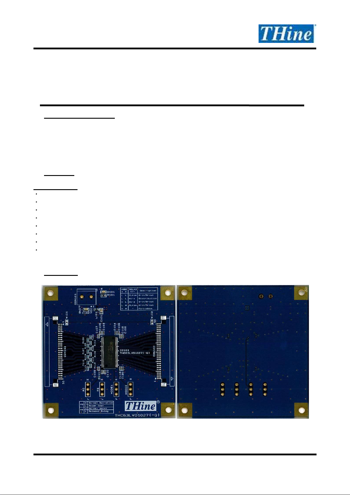
3. Overview
Figure 1 THEVA1027-V2

2/7
THAN0211_Rev.1.00_E
Copyright(C) 2016 THine Electronics, Inc. THine Electronics, Inc.
Securit
y
E
4. Power Supply Setup
This chapter shows power supply condition.
Caution: Please check if there is no power-GND short on below red trace before supplying any power.
3.3V Power Supply to Each Board
Each evaluation board requires 3.3V power supply. Please use “CON1” connector typically.
Figure 2 THEVA1027-V2 power supply for evaluation board
Power Supply from / to Connector
3.3V power supply can be connected to CON103 and CON102 by using W101 and W102 solder jumper.
THEVA1027-V2
W101: Connect the 3.3V power supply with pin#1 and 2 of CON103.
W102: Connect the 3.3V power supply with pin#29 and 30 of CON102.
Figure 3 THEVA1027-V2 power supply from / to each connector

3/7
THAN0211_Rev.1.00_E
Copyright(C) 2016 THine Electronics, Inc. THine Electronics, Inc.
Securit
y
E
5. Function Setting
Setting pin of each board is shown in yellow area of Figure 4.
Figure 4 THEVA1027-V2 position of function setting pin
Pin#2 of each 3HEADER is connected to IC’s setting pin.
Each setting pin’s high or low setting can set by connecting pin#2 of 3HEADER and high level or low level.
(a)3HEADER Description (b)High Level Setting (c)Low Level Setting
Figure 5 Schematic diagram of High / Low setting description
6. Status Indicate LED
LED “D101” indicates 3.3V power supply status.
Setting pins

4/7
THAN0211_Rev.1.00_E
Copyright(C) 2016 THine Electronics, Inc. THine Electronics, Inc.
Securit
y
E
7. Function
This chapter shows function setting of THEVA1027-V2.
Table 1 THEVA1027-V2 function setting description
Silk Symbol Function
PD PD
Power down function setting
H : Normal Operation
L : Power Down Mode (All outputs are Hi-Z)
RS RS
LVDS swing mode.
RS LVDS Swing
H 350mV
L 200mV
MODE1 MODE1
Pixel data mode select
MODE1 MODE0 RCLK2+/- Function
L L Clock input Dual-in / Dual -out
L L Hi-Z Distribution
H L Hi-Z Single-in / Dual -out
L H Clock input Dual-in / Single-out
H H -Reserved
MODE0 MODE0

5/7
THAN0211_Rev.1.00_E
Copyright(C) 2016 THine Electronics, Inc. THine Electronics, Inc.
Securit
y
E
8. Schematic
Figure 6 THEVA1027-V2 Schematic

6/7
THAN0211_Rev.1.00_E
Copyright(C) 2016 THine Electronics, Inc. THine Electronics, Inc.
Securit
y
E
9. Bills of Materials
Table 2 THEVA1027-V2 BOM
10.Set Items
Table 3 THEVA1027-V2 Set Items
TYPE Part No.
DC Connector 282836-2
FFC Connector for LVDS Link 52271-3069
FFC 30pin 1mm Pitch for LVDS Link 98267-0475
It’s possible to mount these parts on this board and use.
Comment Description Value Note Designator Q'ty
Capacitor2012 2012 10uF 16V C101, C102 2
Capacitor1005 1005 0.01uF 16V C103, C104, C111 3
Capacitor1005 1005 0.1uF 16V C105, C106, C107, C108, C109, C110, C120 7
Capacitor1005 1005 4.7nF 16V C118, C119 2
282836-2 282836-2 282836-2(NC) 5mm pitch CON101 1
CN-FFC(1.0)30PD CN-FFC(1.0)30PD 52271-3069(NC) 1mm pitch CON102, CON103 2
LED1608 1608 SML-310MT Green D101 1
3HEAD 3HEAD 3HEAD(NC) 2.54mm pitch Header101, Header102, Header103, Header104 4
THC63LVD1027 TSSOP64 IC101 1
Inductor1608 1608 MPZ1608R471A L101 1
Resistor1608 1608 150 0.1W R101 1
Resistor1005 1005 100 0.1W R102, R103, R104, R105, R106, R107, R108,
R109, R110, R111, R112, R113 12

7/7
THAN0211_Rev.1.00_E
Copyright(C) 2016 THine Electronics, Inc. THine Electronics, Inc.
Securit
y
E
11.Notices and Requests
Please kindly read, understand and accept this “Noticees and Requests” before using this product.
For the Material:
1. The product specifications described in this material are subject to change without prior notice.
2. The circuit diagrams described in this material are examples of the application which may not always
apply to design of respective customers. THine Electronics, Inc. (“THine”) is not responsible for
possible errors and omissions in this material. Please note if the errors or omissions should be found in
this material, THine may not be able to correct them immediately.
3. This material contains THine’s copyright, know-how or other proprietary. Copying or disclosing of the
contents of this material to any third party without THine’s prior permission is strictly prohibited.
For the Product:
1. This product is solely designed for evaluation purpose, and other purposes including mass production
and distribution are not intended.
2. This product has been solely manufactured for electric design engineers but not for end-users.
3. This product is not radiation-tolerant product.
4. This product is presumed to be used for general electric device, not for applications which require
extremely high-reliability/safety (including medical device concerned with critical care, aerospace
device, or nuclear power control device). Also, when using this product for any device concerned with
control and/or safety of transportation mean, traffic signal device, or other various types of safety
device, such use must be after applying appropriate measures to the product.
5. This product has been designed with the utmost care to accomplish the purpose of evaluation of IC
products manufactured by THine Electronics, Inc., however, THine MAKES NO WARRANTIES OR
REPRESENTATIONS WITH REGARD TO ANY PERFORMANCE OR FUNCTION OF THIS
PRODUCT IN ANY CIRCUMSTANCE.
6. This product has been manufactured with the utmost care in quality control and product reliability,
however, there may be faults or defects with a low but fixed probability, as inevitable phenomenon
concerned with semiconductor manufacturing processes. Therefore, Customers are encouraged to have
sufficiently redundant or error-preventive design applied to the use of the product so as not to have
THine’s product cause any social or public damage. Replacement of the product is only available in
case of obvious defects of mount devices at the point of unpacking the product. Neither replacement
nor failure analysis of the product is available in any other case of defects with the product and/or the
product’s components.
7. Customers are asked, if required, to judge by themselves on whether this product falls under the
category of strategic goods under the Foreign Exchange and Foreign Trade Control Law.
8. Please Note that if infringement of any third party’s industrial ownership should occur by using this
product, THine will be exempted from any responsibility unless it directly relates to the production
process or functions of the product.
9. Developing, designing and manufacturing of Customers’ own products, equipments or system by using
of this product is strictly prohibited in any way.
THine Electronics, Inc.
sales@thine.co.jp
This manual suits for next models
2
Table of contents
Other THine Motherboard manuals

THine
THine THSCM101 Guide

THine
THine THCV235 User manual

THine
THine THEVA827 User manual

THine
THine THC63LVD1023B User manual

THine
THine THEVA213-V3 User manual

THine
THine THEVA252-SMA-V1 User manual

THine
THine THSCM101 Guide

THine
THine THSB-FMC-01VX1 User manual

THine
THine THC63LVDM83D User manual

THine
THine THCV215 User manual