THine THEVA252-SMA-V1 User manual

THEVA252-SMA-V1 User’s Guide_Rev.1.22_E
Copyright© 2021, THine Electronics, Inc. THine Electronics, Inc.
SC: E
1
/
20
THEVA252-SMA-V1 User’s Guide
THCS252 Evaluation Kit

THEVA252-SMA-V1 User’s Guide_Rev.1.22_E
Copyright© 2021, THine Electronics, Inc. THine Electronics, Inc.
SC: E
2
/
20
Contennts
THEVA252-SMA-V1 User’s Guide ................................................................................................................. 1
THCS252 Evaluation Kit................................................................................................................................. 1
1. Introduction............................................................................................................................................ 3
1.1 Overview........................................................................................................................................... 3
1.2 Contents of evaluation kit....................................................................................................................... 4
1.3 Quick start guide ................................................................................................................................... 4
2. Details about each part of the board.......................................................................................................... 5
2.1 Power Supply........................................................................................................................................ 5
2.2 Full-duplex high-speed signal connector.................................................................................................. 6
2.2 Pin header and Connector....................................................................................................................... 7
2.3 Silk indication matching......................................................................................................................... 8
3. Schematic and Layout............................................................................................................................... 9
3.1 Circuit diagram...................................................................................................................................... 9
3.2 Layout ................................................................................................................................................ 10
3.2.1 L1(TOP)pattern.......................................................................................................................... 10
3.2.2 L2 pattern .................................................................................................................................. 11
3.2.3 L3 pattern .................................................................................................................................. 12
3.2.4 L4 pattern .................................................................................................................................. 13
3.2.5 TOP side silk.............................................................................................................................. 14
3.2.6 BOTTOM side silk ..................................................................................................................... 15
3.2.7 TOP side implementation ............................................................................................................ 16
3.2.8 BOTTOM side implementation.................................................................................................... 17
3.2.9 Dimensions................................................................................................................................ 18
4. BOM ....................................................................................................................................................... 19

THEVA252-SMA-V1 User’s Guide_Rev.1.22_E
Copyright© 2021, THine Electronics, Inc. THine Electronics, Inc.
SC: E
3
/
20
1. Introduction
1.1 Overview
THEVA252-SMA-V1 is an evaluation board with THCS252 installed. THS252 is a transceiver IC that
aggregates 20bit I/O and allows full-duplex bidirectional communication between master and slave. THEVA252-
SMA-V1 is a single board that supports both master and slave. The board setas the master and slave can be connected
with a coaxial cable via the SMA connector.
If you prepare a conversion board to the desired connector or cable, you can experiment with various transmission
lines. 48-bit connector for 20bit I/O are not mounted.
Figure 1 THEVA252-SMA-V1 Master Side / Slave Side top view
Figure 2 THEVA252-SMA-V1 Master Side / Slave Side bottom view
Down Link
Up Link
20bit I/O
DC
1.8~3.3V
DC
1.8~3.3V
Ext. REF input
20bit I/O
CDR clock output
THCS252 setting THCS252 setting
THCS252 Master side THCS252 Slave side
Down Link
Up Link
THCS252 Master side THCS252 Slave side

THEVA252-SMA-V1 User’s Guide_Rev.1.22_E
Copyright© 2021, THine Electronics, Inc. THine Electronics, Inc.
SC: E
4
/
20
This document describes thefunctions and usageof a pair of boards.If you want to check the operation immediately,
see 1.3 Quick Start Guidelines. Communication at a data rate of about 600Mbps is established.
* DC power supply, four SMA coaxial cables or four SMA connectors, and jumper pins must be prepared.
1.2 Contents of evaluation kit
This evaluation kit includes the contents of Table 1.
Product Article Quantity
THEVA252-SMA-V1 THEVA252-SMA-V1 Board 2
Table 1 THEVA252-SMA-V1 contents
1.3 Quick start guide
1.3.1 Connect the master and slave boards with jumper pin settings as shown in Figure 3 using SMA coaxial cables.
1.3.2 When DC3.3V is supplied to the power supply terminals of both boards, the LED of D1 lights up. The master
board THCS252 internal oscillator starts operating at 20MHz and outputs a downlink signal. When this signal is
received by THCS252 of the slave board and the internal circuit is locked, an uplink signal is output. When this signal
is received by THCS252 of the master board and the internal circuit is locked, communication between the master
and slave is established. When communication is established, THCS252 READY = H and D2 LED lights.
1.3.3. In this state, the built-in oscillator 20MHz operates as the sampling clock, and serialization of 30 times.
Communication is performed at a speed of 600Mbps for both downlink and uplink. * Since this is an internal
oscillator of the LSI, the sampling clock and transmission rate may vary up to +/- 20%.
Figure 3 THEVA252-SMA-V1 Quit start pin setting
SMA Coaxial
Cable or
Connector
DC
1.8~3.3V
DC1
.8~3.3V
D1 LED for Power
D1 LED for Power
D2 READY LED D2 READY LED

THEVA252-SMA-V1 User’s Guide_Rev.1.22_E
Copyright© 2021, THine Electronics, Inc. THine Electronics, Inc.
SC: E
5
/
20
2. Details about each part of the board
2.1 Power Supply
For THEVA252-SMA-V1, there is a method to supply the desired voltage in the range of 1.7V to 3.6V to the
CON1 power terminal block of the master side board and the slave side board. Alternatively, pins 1, 2, and 3 of 48-
pin PH8 can be connected to CON1 via JP1 on the bottom of the board, power can be shared from the front and rear
circuits via pins 1, 2, and 3 of PH8 is possible.
Figure 4 THEVA252-SMA-V1 Power supply
Figure 5 THEVA252-SMA-V1 Power sharing

THEVA252-SMA-V1 User’s Guide_Rev.1.22_E
Copyright© 2021, THine Electronics, Inc. THine Electronics, Inc.
SC: E
6
/
20
2.2 Full-duplex high-speed signal connector
THEVA252-SMA-V1 uses SMAconnectors for high-speed signal input / output.
Figure 6 THEVA252-SMA-V1 High Speed CML I/O connector
SMA Connector
SMAJ103-T16 Land pattern
SMA Connector
SMAJ103-T16 Mounting image
THEVA252-SMA-V1 User’s Guide_Rev.1.22_E
Copyright© 2021, THine Electronics, Inc. THine Electronics, Inc.
SC: E
7
/
20
2.2 Pin header and Connector
* PH8 is not mounted.
PH8 48-pin layout has 20 pins for I/O, 1 pin for external REF input (master) / CDR clock output (slave), 3 pins for
power supply sharing, and 24 pins for GND. Connect the I/O circuits on the master side and slave side according to
the THCS252 mode setting.
Chip Master Side Chip Slave Side
Figure 7 THEVA252-SMA-V1 Pin header for I/O_PH8
1 VCC VCC VCC 3
4 GND GND GND 6
7 GND GND GND 9
10 D0 / D19 D1 / D18 D2 / D17 12
13 D3 / D16 D4 / D15 D5 / D14 15
16 D6 / D13 D7 / D12 D8 / D11 18
19 D9 / D10 GND GND 21
22 GND GND GND 24
25 GND GND GND 27
28 GND GND GND 30
31 GND D10 / D9 D11 / D8 33
34 D12 / D7 D13 / D6 D14 / D5 36
37 D15 / D4 D16 / D3 D17 / D2 39
40 D18 / D1 D19 / D0 CLK 42
43 GND GND GND 45
46 GND GND GND 48
48 GND GND GND 46
45 GND GND GND 43
42 CLK D19 / D0 D18 / D1 40
39 D17 / D2 D16 / D3 D15 / D4 37
36 D14 / D5 D13 / D6 D12 / D7 34
33 D11 / D8 D10 / D9 GND 31
30 GND GND GND 28
27 GND GND GND 25
24 GND GND GND 22
21 GND GND D9 / D10 19
18 D8 / D11 D7 / D12 D6 / D13 16
15 D5 / D14 D4 / D15 D3 / D16 13
12 D2 / D17 D1 / D18 D0 / D19 10
9 GND GND GND 7
6 GND GND GND 4
3 VCC VCC VCC 1

THEVA252-SMA-V1 User’s Guide_Rev.1.22_E
Copyright© 2021, THine Electronics, Inc. THine Electronics, Inc.
SC: E
8
/
20
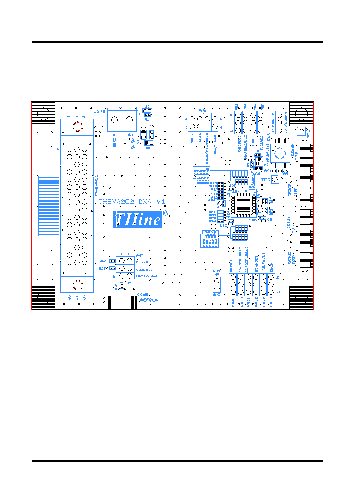
2.3 Silk indication matching
Some of the silk indication of THEVA252-SMA-V1 is inconsistent with the schematic indication and the terminal
name symbol of the data sheet. The table below shows the consistency of the notation.
Silk indication Circuit diagram indication and
data sheet symbols
Remarks
SCL1 OPT0 (Schematic)
Not listed in the data sheet
PH1, Not used.
SDA1 OPT1(Schematic)
Not listed in the data sheet
PH1 Not used.
SCL0/FILTSEL0 FILTSEL0 PH1
SDA0/SSEN SSEN PH1
ENI2C0 RESERVED PH5, Used with L fixed
ID/DIR_SEL0 DIRSEL0 PH10
ID/DIR_SEL1 DIRSEL1 PH11
THEVA252-SMA-V1 User’s Guide_Rev.1.22_E
Copyright© 2021, THine Electronics, Inc. THine Electronics, Inc.
SC: E
9
/
20
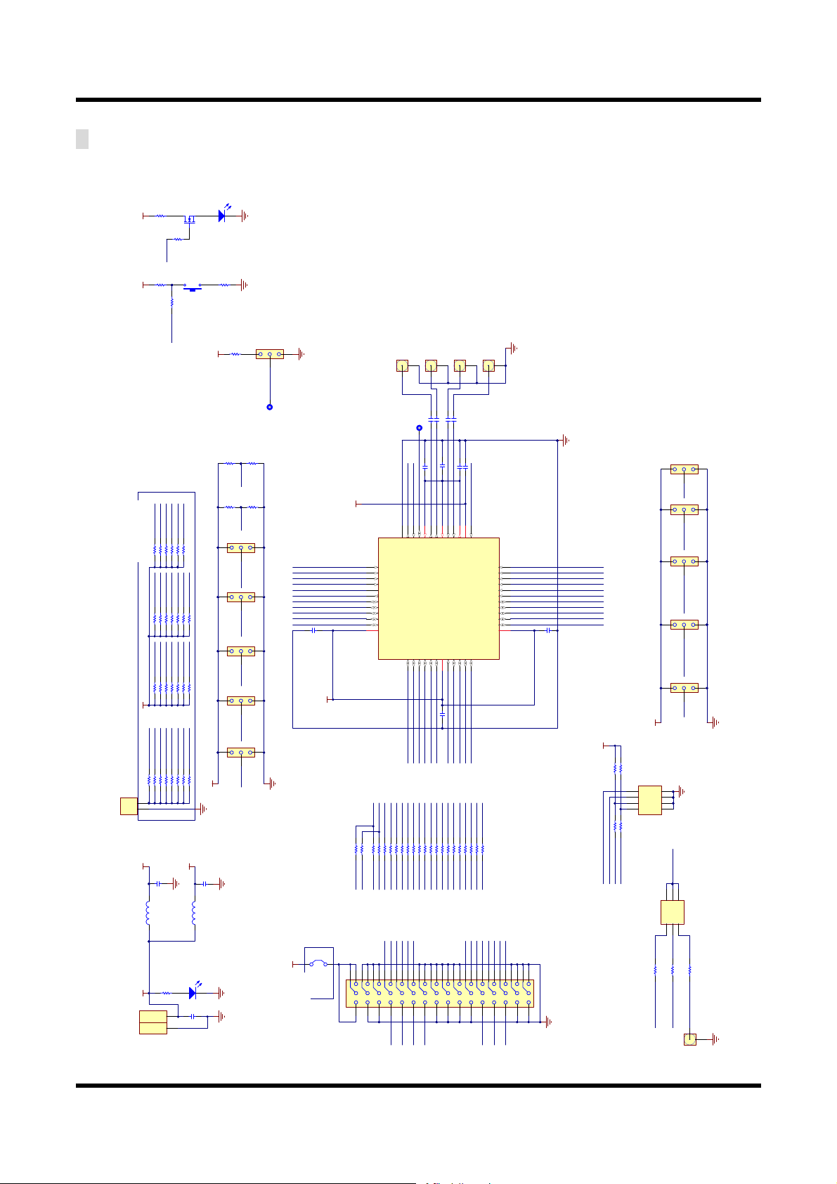
3. Schematic and Layout
3.1 Circuit diagram.
1
2
CON2
SMA(NC)
GND
50ohm
1
2
CON3
SMA(NC)
50ohm
1
2
CON4
SMA(NC)
50ohm
1
2
CON5
SMA(NC)
D6
D7
D8
D9
D10
D11
D12
D13
D14
D15
D16
D17
REFEN
DIRSEL0
D18
D19
CLK/OSCSEL
DIRSEL1
AVDD
CAP
STANDBY
TEST2
CAP
INT/LOCKN
TXP
TXN
RESETN
TEST1
AVDD
VDD
1
20
2
3
45
6
78
9
10 11
12
13 14
15
16 17
18
19
30
29
28
27
26
25
24
23
22
21
40
39
38
37
36
35
34
33
32
31
48
47
46
45
44
43
42
41
3x16
PH8-NC1
GND
D1_C
D2_C
D4_C
D5_C
D19_C
D12_C
D15_C
D18_C
D7_C
D8_C
D10_C
D11_C
D13_C
D14_C
D16_C
D17_C
D0_C
D3_C
D6_C
D9_C
Solder Jumper JP1
D5
D4
D3
D1
D2
D0
FILTSEL0
SSEN
READY
RF/OSCSEL0
MSSEL
0.1uFC9
0.1uFC12
FILTSEL1 RESERVED
RXN
RXP
1
2GND
VCC
CON1
3.3V Power Supply
10uF
C1
GND
3.3V_VCC
GREEN
D1
GND
VDD
10uF
C2
GND AVDD
10uF
C11
GND
CLK_PH
3.3V_VCC
10uFC14
0.1uFC13
OBUF
D0_C D0
D1_C D1
D2_C D2
D3_C D3
D4_C D4
D5_C D5
D6_C D6
D7_C D7
D8_C D8
D9_C D9
D10_C D10
D11_C D11
D12_C D12
D13_C D13
D14_C D14
D15_C D15
D16_C D16
D17_C D17
D18_C D18
D19_C D19
D0
D1
D2
D3
D4
D5
D6
D7
D8
D9
D10
D11
D12
D13
D14
D15
D16
D17
D18
D19
470ohm@100MHz
L1
10kΩR47
10kΩR46
10kΩR45
10kΩR44
10kΩR43
10kΩR52
10kΩR53
VDD
GND
150Ω
R1
0.1uFC6
0.1uF
C10 0.1uF
C3
470ohm@100MHz
L2
33ΩR10
33ΩR9
33ΩR8
33ΩR7
33ΩR6
33ΩR15
33ΩR16
33ΩR17
33ΩR18
33ΩR19
33ΩR20
33ΩR22
33ΩR23
33ΩR24
33ΩR29
33ΩR30
33ΩR31
33ΩR32
33ΩR33
33ΩR21
10kΩR56
10kΩR57
10kΩR58
10kΩR59
10kΩR60
10kΩR61
10kΩR62
10kΩR63
10kΩR64
10kΩR65
10kΩR66
10kΩR67
10kΩR68
REFEN DIRSEL0 DIRSEL1 OBUF
VDD
STANDBY
1
2
3
PH9
1
2
3
PH10
1
2
3
PH11
1
2
3
PH12
1
2
3
PH14
GND
1
2
50ohm
CON6
SMA(NC)
CLK_PH
CLK/OSCSEL
REFIN_SMA
GND
OSCSEL1 1
2
3
4
5
6
PH733ΩR34
0ΩR35
0ΩR36
READY
GREEN
D2
GND
RESETN
GND
Q1
MOSFET-N
VDDVDD
SW1
Push-Switch
10kΩ
R5
0ΩR4
0Ω
R42
150Ω
R2
0Ω
R3
0.1uFC4 0.1uFC5
0.1uFC7 0.1uFC8
FILTSEL0
SSEN
OPT0
OPT1 VDD
GND
0ΩR49
0ΩR48
0ΩR39
0ΩR40 10kΩR41 10kΩR38
1
2
3
4
5
6
7
8
PH1
OSCSEL1 RESERVEDFILTSEL1RF/OSCSEL0 MSSEL
1
2
3
PH2
VDD
GND
1
2
3
PH3
1
2
3
PH13
1
2
3
PH5
1
2
3
PH4
OPT1
OPT0
D16
D17
D18
D19
D0
D1
D2
D3
10kΩ(NC)R14
10kΩ(NC)R13
10kΩ(NC)R12
10kΩ(NC)R11
10kΩ(NC)R25
10kΩ(NC)R26
10kΩ(NC)R27
10kΩ(NC)R28
1
2
PH8
Torrelant I/O pull-up voltage supply
GND
Bottom Side
Bottom Side
TEST2
TEST1 0Ω(NC)
R55
0Ω
R51
0Ω(NC)
R54
0Ω
R50
TP2
1
2
3
PH6
INT/LOCKN
GND
10KΩ
R37
VDD
TP1
CAP
RESERVED 1
MSSEL 2
RF / OSCSEL0 3
READY 4
SSEN 5
FILTSEL0 6
D0 / D19 7
D1 / D18 8
D2 / D17 9
D3 / D16 10
D4 / D15 11
VDD 12
D5 / D14
13
D6 / D13
14
D7 / D12
15
D8 / D11
16
D9 / D10
17
D10 / D9
18
VDD
19
REFIN / REFOUT / OSCSEL1
20
D11 / D8
21
D12 / D7
22
D13 / D6
23
D14 / D5
24
VDD
25
D15 / D4
26
D16 / D3
27
D17 / D2
28
D18 / D1
29
D19 / D0
30
REFEN
31
DIRSEL0
32
DIRSEL1
33
STANDBY
34
FILTSEL1
35
OBUF
36
TEST2 37
AVDD 38
CAPOUT 39
RXP 40
RXN 41
CAPINA 42
TXN 43
TXP 44
CAPINP 45
INT / LOCKN 46
TEST1 47
RESETN 48
EXP GND 49
IC
THCS252

THEVA252-SMA-V1 User’s Guide_Rev.1.22_E
Copyright© 2021, THine Electronics, Inc. THine Electronics, Inc.
SC: E
10
/
20
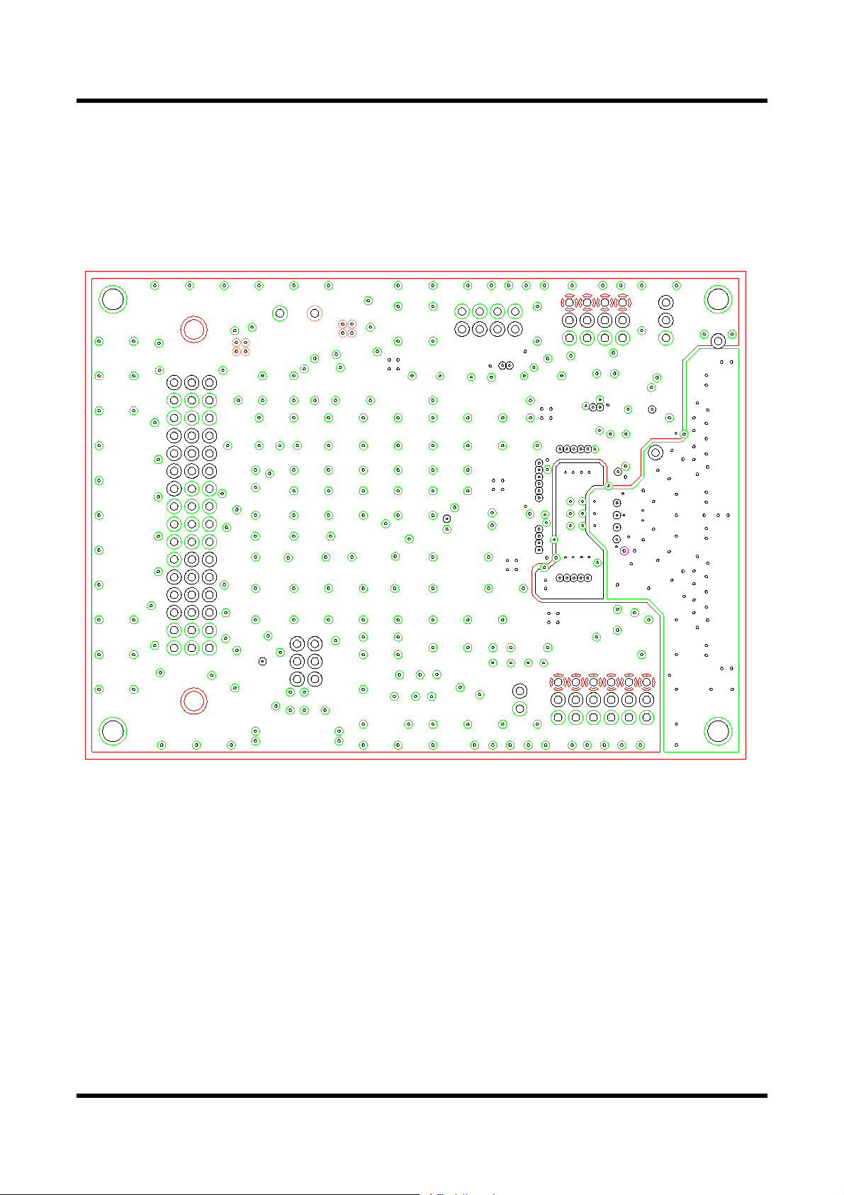
3.2 Layout
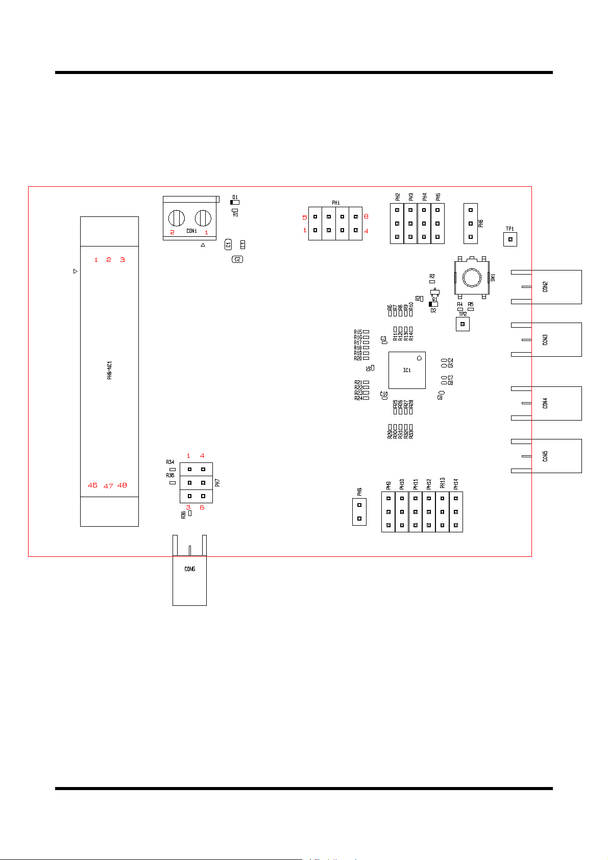
3.2.1 L1(TOP)pattern

THEVA252-SMA-V1 User’s Guide_Rev.1.22_E
Copyright© 2021, THine Electronics, Inc. THine Electronics, Inc.
SC: E
11
/
20
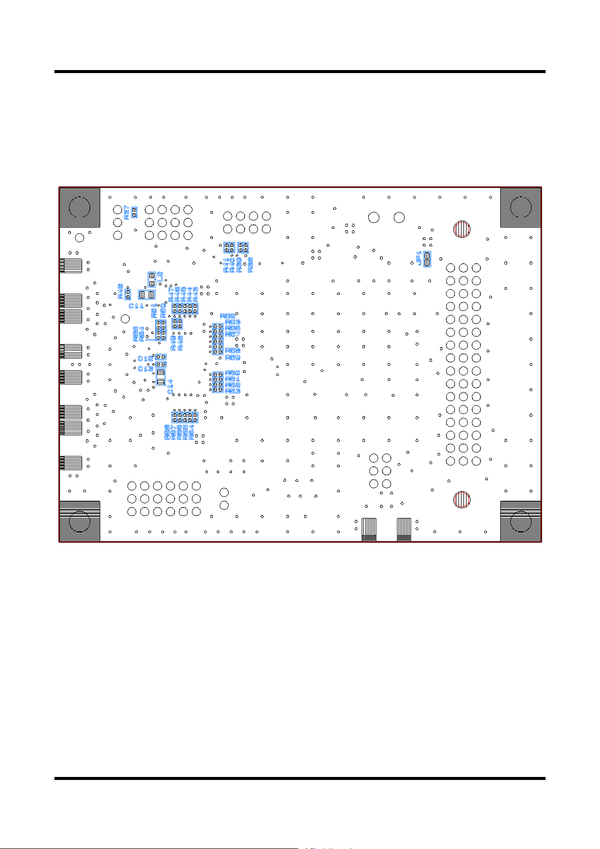
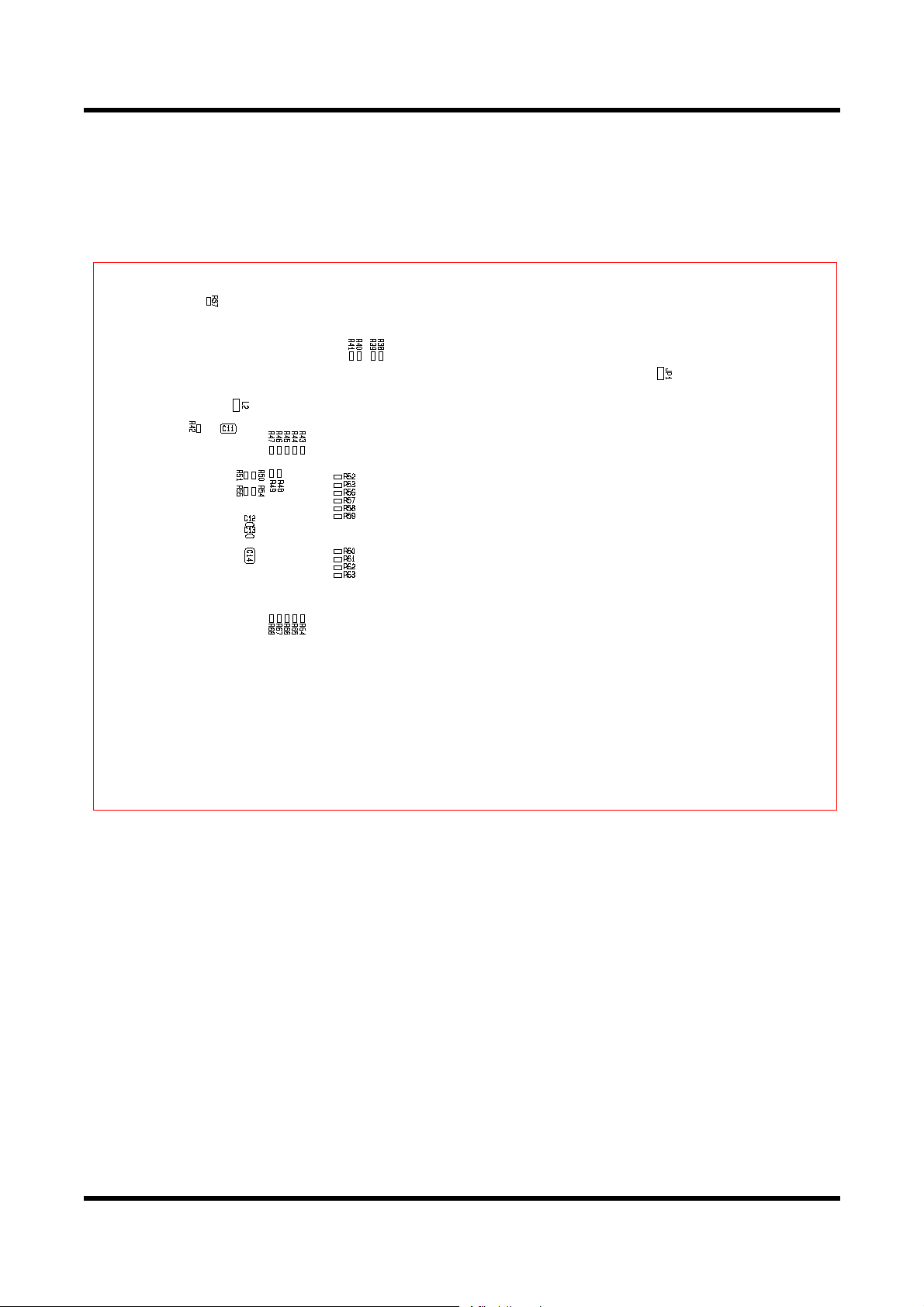
3.2.2 L2 pattern
THEVA252-SMA-V1 User’s Guide_Rev.1.22_E
Copyright© 2021, THine Electronics, Inc. THine Electronics, Inc.
SC: E
12
/
20
3.2.3 L3 pattern
THEVA252-SMA-V1 User’s Guide_Rev.1.22_E
Copyright© 2021, THine Electronics, Inc. THine Electronics, Inc.
SC: E
13
/
20
3.2.4 L4 pattern
THEVA252-SMA-V1 User’s Guide_Rev.1.22_E
Copyright© 2021, THine Electronics, Inc. THine Electronics, Inc.
SC: E
14
/
20
3.2.5 TOP side silk
THEVA252-SMA-V1 User’s Guide_Rev.1.22_E
Copyright© 2021, THine Electronics, Inc. THine Electronics, Inc.
SC: E
15
/
20
3.2.6 BOTTOM side silk
THEVA252-SMA-V1 User’s Guide_Rev.1.22_E
Copyright© 2021, THine Electronics, Inc. THine Electronics, Inc.
SC: E
16
/
20
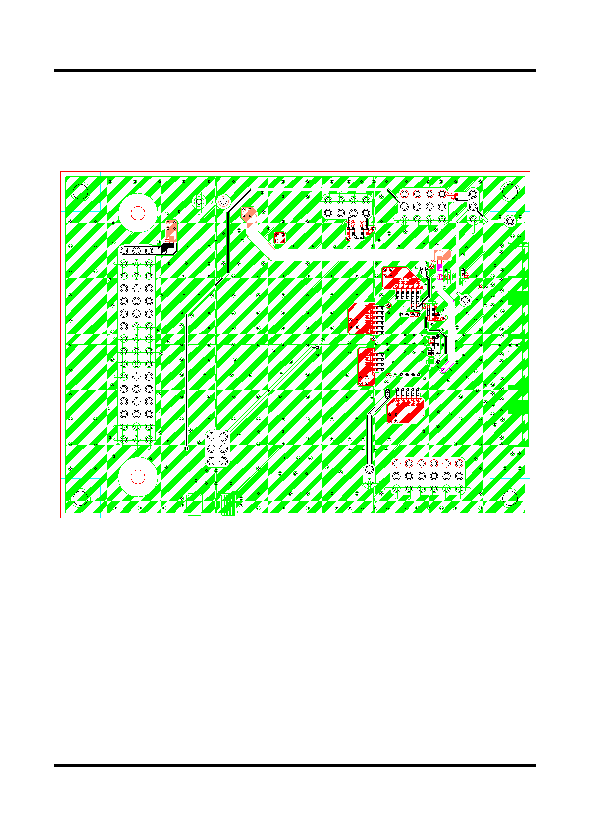
3.2.7 TOP side implementation
THEVA252-SMA-V1 User’s Guide_Rev.1.22_E
Copyright© 2021, THine Electronics, Inc. THine Electronics, Inc.
SC: E
17
/
20
3.2.8 BOTTOM side implementation
THEVA252-SMA-V1 User’s Guide_Rev.1.22_E
Copyright© 2021, THine Electronics, Inc. THine Electronics, Inc.
SC: E
18
/
20
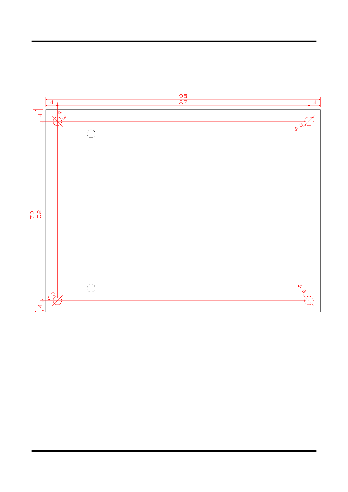
3.2.9 Dimensions
THEVA252-SMA-V1 User’s Guide_Rev.1.22_E
Copyright© 2021, THine Electronics, Inc. THine Electronics, Inc.
SC: E
19
/
20
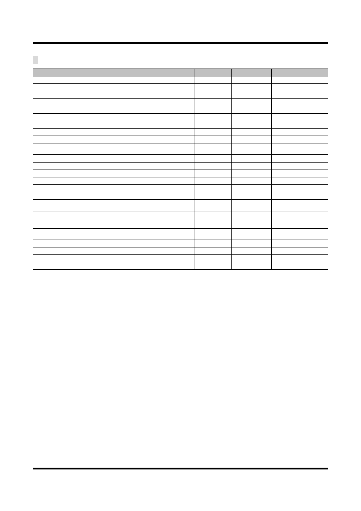
4. BOM
Designator Description Value Quantity P/N
C1, C2, C11, C14 Cap. 2012 10uF 4 GRM21BB31C106KE15L
C3, C4, C5, C6, C7, C8, C9, C10, C12, C13 Cap. 1005 0.1uF 10 GRM155B31E104KA87D
CON1 Terminal_Block 2pin 1 282836-2
CON2, CON3, CON4, CON5, CON6 SMA 50ohm 5 SMA103-T16
D1, D2 LED GREEN 2 SML-D12P8WT86
IC1 QFN48 1
JP1 Jumper(NC) Solder Jumper 1
L1, L2 Coil. 1608
470ohm@100MHz
2 MPZ1608B471ATA00
PH1 Header 8 2x4 1 TCHM23-70-008S-803R
PH2, PH3, PH4, PH5, PH9, PH10, PH11, PH12,
PH13, PH14 Header 3 1x3 10 TCHM13-70-003S-803R
PH6 Header 3 1x3 1 TCHM13-70-003S-803R
PH7 Header 6 2x3 1 TCHM23-70-006S-803R
PH8 Header 2 1x2 1 TCHM13-70-002S-803R
PH8-NC1 Header 48(NC) 3x16(NC) 1 PCN10-48P-2.54DSA(72)
Q1 MOSFET N-ch 1 SSM3K16FS
R1, R2 Res. 1005 150Ω 2 RK73H1ETTP1500F
R3, R4, R35, R36, R39, R40, R42, R48, R49, R50,
R51 Res. 1005, Res. 1005(NC) 0Ω 11 RK73Z1ETTP0
R5, R37, R38, R41, R43, R44, R45, R46, R47, R52,
R53, R56, R57, R58, R59, R60, R61, R62, R63, R64,
R65, R66, R67, R68
Res. 1005 10kΩ 24 RK73H1ETTP1002F
R6, R7, R8, R9, R10, R15, R16, R17, R18, R19, R20,
R21, R22, R23, R24, R29, R30, R31, R32, R33, R34 Res. 1005 33Ω 21 RK73H1ETTP33R0F
R11, R12, R13, R14, R25, R26, R27, R28 Res. 1005(NC) 10kΩ(NC) 8 RK73H1ETTP1002F
R54, R55 Res. 1005(NC) 0Ω(NC) 2 RK73Z1ETTP0
SW1 SW Top Push 1 SKHMQKE010
TP1, TP2 Test Point(NC) Through hole 2

THEVA252-SMA-V1 User’s Guide_Rev.1.22_E
Copyright© 2021, THine Electronics, Inc. THine Electronics, Inc.
SC: E
20
/
20
Notices and requests
Please kindly read, understand and accept this “Notices and Requests” before using this product.
For the Material:
1. The product specifications described in this material are subject to change without prior notice.
2. The circuit diagrams described in this material are examples of the application which may not always apply to
design of respective customers. THine Electronics, Inc. (“THine”) is not responsible for possible errors and
omissions in this material. Please note even if the errors or omissions should be found in this material, THine
may not be able to correct them immediately.
3. This material contains THine’s copyright, know-how or other proprietary. Copying or disclosing of the contents
of this material to any third party without THine’s prior permission is strictly prohibited.
For the Product:
1. This product is solely designed for evaluation purpose, and other purposes including mass production and
distribution are not intended.
2. This product has been solely manufactured for electric design engineers but not for end-users.
3. This product is not radiation-tolerant product.
4. This product is presumed to be used for general electric device, not for applications which require extremely
high-reliability/safety (including medical device concerned with critical care, aerospace device, or nuclear power
control device). Also, when using this product for any device concerned with control and/or safety of
transportation means, traffic signal device, or other various types of safety device, such use must be after
applying appropriate measures to the product.
5. This product has been designed with the utmost care to accomplish the purpose of evaluation of IC products
manufactured by THine Electronics, Inc. (“THine”); however, THine MAKES NO WARRANTIES OR
REPRESENTATIONS WITH REGARD TO ANY PERFORMANCE OR FUNCTION OF THIS PRODUCT IN
ANY CIRCUMSTANCES.
6. This product has been manufactured with the utmost care in quality control and product reliability; however,
there may be faults or defects with a low but fixed probability, as inevitable phenomenon concerned with
semiconductor manufacturing processes. Therefore, customers are encouraged to have sufficiently redundant or
error-preventive design applied to the use of the product so as not to have THine’s product cause any social or
public damage. Neither replacement nor failure analysis of the product is available in any case of defects with the
product and/or the product’s components.
7. Customers are asked, if required, to judge by themselves on whether this product falls under the category of
strategic goods under the Foreign Exchange and Foreign Trade Act.
8. Please Note that even if infringement of any third party’s industrial ownership should occur by using this
product, THine will be exempted from any responsibility unless it directly relates to the production process or
functions of the product.
9. Developing, designing and manufacturing of customers’ own products, equipment or system by using of this
product is strictly prohibited in any way.
Table of contents
Other THine Motherboard manuals

THine
THine THSCM101 Guide

THine
THine THC63LVD1023B User manual

THine
THine THC63LVD1027D User manual

THine
THine THSB-FMC-01VX1 User manual

THine
THine THC63LVD1023B User manual

THine
THine THEVA827 User manual

THine
THine THCV235 User manual

THine
THine THC63LVDM83D User manual

THine
THine THEVA213-V3 User manual

THine
THine THC63LVD1027 User manual


 series user manual")


