THine THEVA827 User manual

THAN0210_Rev.1.00_E
1/7
Copyright(C) 2016 THine Electronics, Inc. THine Electronics, Inc.
Securit
y
E
THC63LVD827(-Q) Evaluation Kit
LVDS Dual Link Evaluation Board
Parts Number: THEVA827
1. General Description
THEVA827 is designed to evaluate THC63LVD827(-Q) for transmission video data.
THC63LVD827(-Q) chipset can transmit 24bit RGB data and HS/VS/DE sync via dual channel LVDS.
The maximum clock frequency of THC63LVD827(-Q) is 174MHz.
2. Features
THC63LVD827
・Low power 1.8V CMOS design (1.8~3.3V IO voltage supported)
・Power down mode
・Wide dot clock range suited for TV signal(480i to 1080p), PC signal(VGA to WUXGA)
・PLL requires no external components
・Clock edge selectable
・Single TTL in, Single/Dual LVDS (Open-LDI) out
・Double Edge Input(Single in/Dual out Mode)
・Additional 6bit only low power mode
・2 LVDS Data Mapping Modes
・Pseudo Random Pattern Generation Circuit
・Support Reduced Swing LVDS for Lower EMI
・TFBGA 72 Pin 7x7mm 0.65mm pitch
3. Overview
Figure 1 THEVA827
2/7
THAN0210_Rev.1.00_E
Copyright(C) 2016 THine Electronics, Inc. THine Electronics, Inc.
Securit
y
E
4. Power Supply Setup
This chapter shows power supply condition.
Caution: Please check if there is no power-GND short on below red trace before supplying any power.
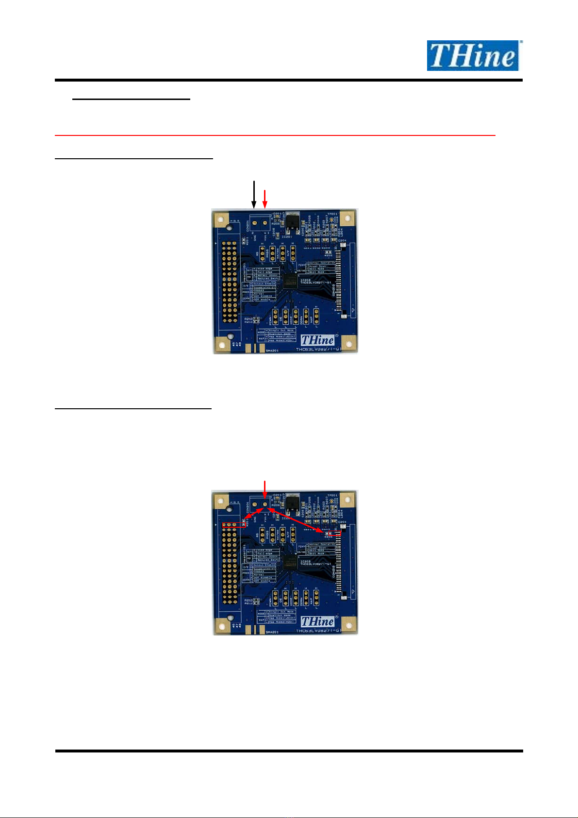
1.8~3.3V Power Supply to the Board
Evaluation board requires 1.8~3.3V power supply. Please use “CON201” connector typically.
Figure 2 THEVA827 power supply for evaluation board
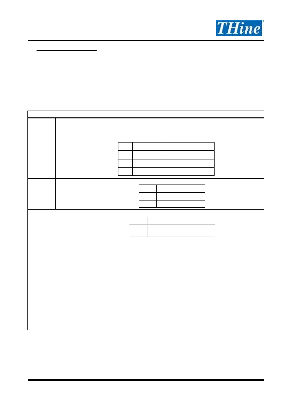
Power Supply from / to Connector
power supply can be connected to Header201 and CON202 by using W201 and W202 solder jumper.
THEVA827
W201: Connect the power supply with pin#1, 2 and 3 of Header201.
W202: Connect the power supply with pin#29 and 30 of CON202.
Figure 3 THEVA827 power supply from / to each Connector
1.8~3.3V power supply
Ground

3/7
THAN0210_Rev.1.00_E
Copyright(C) 2016 THine Electronics, Inc. THine Electronics, Inc.
Securit
y
E
5. Function Setting
Setting pin of the board is shown in yellow area of Figure 4.
Figure 4 THEVA827 position of function setting pins
Pin#2 of each 3HEADER is connected to IC’s setting pin.
Each setting pin’s high or low setting can set by connecting pin#2 of 3HEADER and high level or low level.
(a)3HEADER Description (b)High Level Setting (c)Low Level Setting
Figure 5 Schematic diagram of High / Low setting description
6. Clock Input from SMA Connector
THEVA827 can also choose the TTL clock input from SMA connector by using 0ohm resistor. If you want to
use SMA connector for clock input, please change the 0ohm resistor mount from R210 to R211.
Figure 6 THEVA827 TTL clock input connector select
Setting pins
4/7
THAN0210_Rev.1.00_E
Copyright(C) 2016 THine Electronics, Inc. THine Electronics, Inc.
Securit
y
E
7. Status Indicate LED
LED “D201” indicates power supply status.
8. Function
This chapter shows function setting of THEVA827.
Table 1 THEVA827 Function Setting Description
Silk Symbol Function
R/F R/F
Input clock triggering edge select.
H : Rising Edge
L : Falling Edge
RS RS
LVDS swing mode, VREF select.
RS LVDS Swing Small Swing Input Support
VIHM 350mV N / A
VIMM 350mV RS = VREF
VILM 200mV N / A
MAP MAP
LVDS mapping table select
MAP Mapping Mode
H Mapping MODE1
L Mapping MODE2
MODE MODE
Pixel data mode select
MODE Function
H Single Link (Single-in / Single-out)
L Dual Link (Single-in / Dual -out)
O/E OE
Output enable
H : Output Enable
L : Output Disable (all outputs are Hi-Z)
/PDWN PDWN
Power down function setting
H : Normal Operation
L : Power Down Mode (All outputs are Hi-Z)
PRBS PRBS
PRBS (Pseudo Random Binary Sequence) generator is active for evaluation purposer
H : PRBS Generator Enable
L : Normal Operation
6B/8B 6B/8B
6bit / 8bit mode select
H : 6bit mode (21bit mode)
L : 8bit mode (27bit mode)
DDRN DDRN
DDR enable when MODE=L (Dual out mode), Negative active polarity
H : DDR (Double Edge input) function disable
L : DDR (Double Edge input) function enable
5/7
THAN0210_Rev.1.00_E
Copyright(C) 2016 THine Electronics, Inc. THine Electronics, Inc.
Securit
y
E
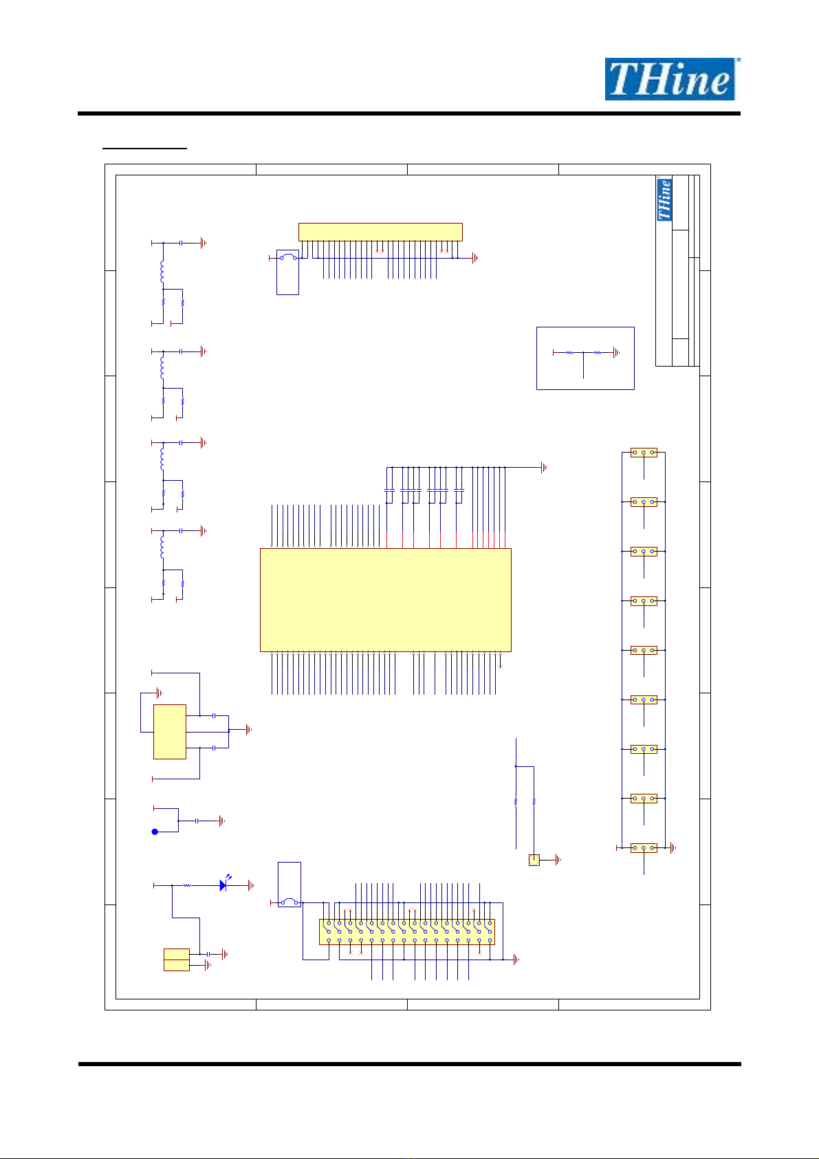
9. Schematic
Figure 7 THEVA827 Schematic
1
1
2
2
3
3
4
4
5
5
6
6
7
7
8
8
D D
C C
B B
A A
Title
Number RevisionSize
A3
Date: 2 16/ 3/ 7 Sheet of
File: C:\Users\..\THEVA827-Q_R1 .SchDoc Drawn By:
THEVA827(-Q)
1.
1 1
GND 1 uF
C2 6
GND
VDD
SML-31 MT
D2 1
15 Ω
R2 9
GND
VDD
MPZ16 8R471A
L2 1
1 uF
C2 1
GND
VDD
MPZ16 8R471A
L2 2
1 uF
C2 2
GND
1
2
2
3
4
5
6
7
8
9
1
11
12
13
14
15
16
17
18
19
3
29
28
27
26
25
24
23
22
21
4
39
38
37
36
35
34
33
32
31
48
47
46
45
44
43
42
41
PCN1 -48P-2.54DS_2(NC)
Header2 1
VDD
GND
R2
R3
G2
G3
B4
B5
B6
B7
B8
B9
HSYNC
VSYNC
DE
G9
R4
R5
R6
R7
R8
R9
G4
G5
G6
G7
G8
CLKIN1_CON
B2
B3
VCC LVDSVCC VDD
MPZ16 8R471A
L2 3
1 uF
C2 3
GND
PLLVCC
Solder Jumper
W2 1
52271-3 69(NC)
1
2
3
4
5
6
7
8
9
1
11
12
13
14
15
16
17
18
19
2
21
22
23
24
25
26
27
28
29
3 CON2 2
TD1+
TD1-
TCLK1+
TCLK1-
TC1+
TC1-
TB1+
TB1-
TA1+
TA1-
VDD
GND
TD2+
TD2-
TCLK2+
TCLK2-
TC2+
TC2-
TB2+
TB2-
TA2+
TA2-
Solder Jumper
W2 2
TD1+
TD1-
TCLK1+
TCLK1-
TC1+
TC1-
TB1+
TB1-
TA1+
TA1-
TD2+
TD2-
TCLK2+
TCLK2-
TC2+
TC2-
TB2+
TB2-
TA2+
RS
R2
R3
G2
G3
B4
B5
B6
B7
B8
B9
G9
R4
R5
R6
R7
R8
R9
G4
G5
G6
G7
G8
B2
B3
DE
VSYNC
HSYNC
CLKIN
Reserved1
PDWN
OE
R/F
PRBS
MODE
MAP
DDRN
6B/8B
1
2
3
3HEAD(NC)
Header2 2
1
2
3
3HEAD(NC)
Header2 3
1
2
3
3HEAD(NC)
Header2 4
GND
RS PDWN OE
IOVCC
1
2
3
3HEAD(NC)
Header2 5
1
2
3
3HEAD(NC)
Header2 6
1
2
3
3HEAD(NC)
Header2 7
1
2
3
3HEAD(NC)
Header2 8
1
2
3
3HEAD(NC)
Header2 9
DDRNMODE MAP R/FPRBS
1
2
3
3HEAD(NC)
Header21
6B/8B
Ω(NC)
R212
Ω
R213
Reserved1
GND
VDD
MPZ16 8R471A
L2 4
1 uF
C2 4
GND
IOVCC
TA2-
.1uFC218
.1uF
C22
GND
R17
G1
R16
G2
R15
F1
R14
F2
R13
E1
R12
E2
R11
D1
R1
D2
G17
J4
G16
H4
G15
J3
G14
H3
G13
J2
G12
H2
G11
J1
G1
H1
B17
J8
B16
H8
B15
J7
B14
H7
B13
J6
B12
H6
B11
J5
B1
H5
DE
G9
VSYNC
H9
HSYNC
J9
CLKIN
F9
RS
F8
Reserved1
C3
/PDWN
D8
O/E
D9
R/F
G8
PRBS
C1
MODE
E7
MAP
E8
DDRN
E9
6B/8B
F7
N/C
C2
TA1+ A1
TA1- B1
TB1+ A2
TB1- B2
TC1+ A3
TC1- B3
TCLK1+ A4
TCLK1- B4
TD1+ A5
TD1- B5
TA2+ A6
TA2- B6
TB2+ A7
TB2- B7
TC2+ A8
TC2- B8
TCLK2+ A9
TCLK2- B9
TD2+ C9
TD2- C8
PLLVCC C7
LVDSVCC C5
LVDSVCC D3
IOVCC G7
VCC G3
VCC G5
GND C4
GND C6
GND D7
GND E3
GND F3
GND G4
GND G6
IC2 2 THC63LVD827
. 1uF
C219
. 1uF
C217
. 1uF
C215
.1uF
C216
.1uF
C214
. 1uF
C213
.1uF
C212
. 1uF
C211
.1uF
C21
. 1uF
C2 9
282836-2(NC)
1
2GND
VDD
CON2 1
Ω(NC)
R2 8
VDD2 Ω
R2 4
TP2 1 VDD2
1 uF
C2 5
GND
VCC
IOVCC
VCC
LVDSVCC
LVDSVCC
PLLVCC
1
2
SMA1 3-T16(NC)
SMA2 1 Ω(NC)R211
CLKIN1_CON ΩR21 CLKIN
CLKIN1_SMA
GND
INPUT
1
GND
2
OUTPUT
3
GND 4
IC2 1
uPC2918BT
GND
1 uF
C2 7
1 uF
C2 8
GND
VDD1.8
VDD
Ω
R2 7
Ω(NC)
R2 3
Ω
R2 6
Ω(NC)
R2 2
Ω
R2 5
Ω(NC)
R2 1
VDD1.8 VDD1.8 VDD1.8
IOVCC
6/7
THAN0210_Rev.1.00_E
Copyright(C) 2016 THine Electronics, Inc. THine Electronics, Inc.
Securit
y
E
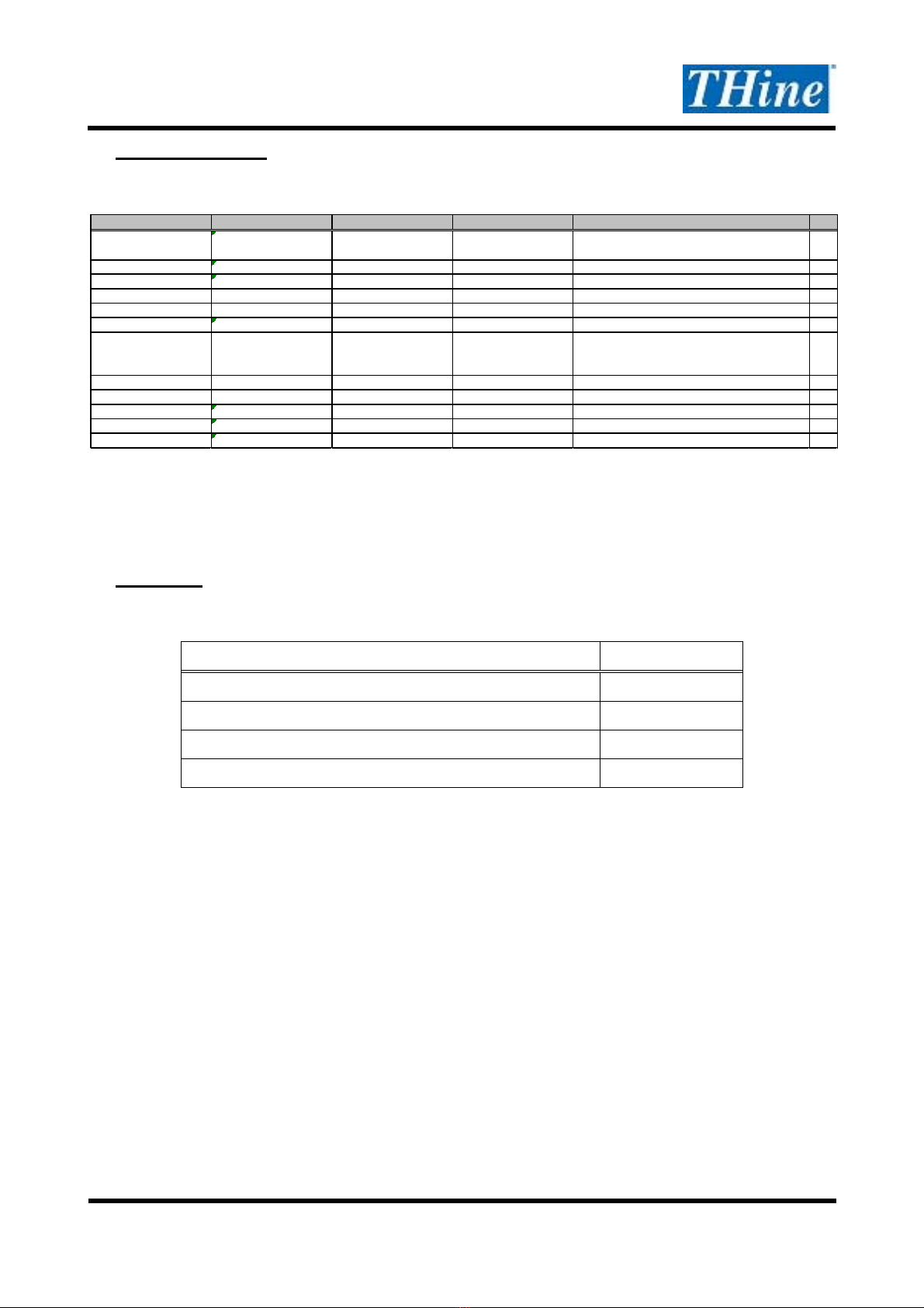
10.Bill of Materials
Table 2 THEVA827 BOM
11.Set Items
Table 3 Set Items
TYPE Part No.
DC Connector 282836-2
FFC Connector for LVDS Link 52271-3069
FFC 30pin 1mm Pitch for LVDS Link 98267-0475
Pin Header ---
It’s possible to mount these parts on this board and use.
Comment Description Value Note Designator Q'ty
Capacitor2012 2012 10uF 16V C201, C202, C203, C204, C205, C206, C207,
C208 8
Capacitor1005 1005 0.01uF 16V C209, C211, C213, C215, C217, C219 6
Capacitor1005 1005 0.1uF 16V C210, C212, C214, C216, C218, C220 6
282836-2 282836-2 282836-2(NC) 5mm pitch CON201 1
CN-FFC(1.0)30PD CN-FFC(1.0)30PD 52271-3069(NC) 1mm pitch CON202 1
LED1608 1608 SML-310MT Green D201 1
3HEA D 3HEA D 3HEA D(NC) 2.54mm pitch
Header202, Header203, Header204, Header205,
Header206, Header207, Header208, Header209,
Header210
9
uPC2918BT SC-63 IC201 1
THC63LVD827 TFBGA72 IC202 1
Inductor1608 1608 MPZ1608R471A L201, L202, L203, L204 4
Resistor1608 1608 0ohm 1A(0ohm) R205, R206, R207, R204, R210, R213 6
Resistor1608 1608 150Ω0.1W R209 1

7/7
THAN0210_Rev.1.00_E
Copyright(C) 2016 THine Electronics, Inc. THine Electronics, Inc.
Securit
y
E
12.Notices and Requests
Please kindly read, understand and accept this “Noticees and Requests” before using this product.
For the Material:
1. The product specifications described in this material are subject to change without prior notice.
2. The circuit diagrams described in this material are examples of the application which may not always
apply to design of respective customers. THine Electronics, Inc. (“THine”) is not responsible for
possible errors and omissions in this material. Please note if the errors or omissions should be found in
this material, THine may not be able to correct them immediately.
3. This material contains THine’s copyright, know-how or other proprietary. Copying or disclosing of the
contents of this material to any third party without THine’s prior permission is strictly prohibited.
For the Product:
1. This product is solely designed for evaluation purpose, and other purposes including mass production
and distribution are not intended.
2. This product has been solely manufactured for electric design engineers but not for end-users.
3. This product is not radiation-tolerant product.
4. This product is presumed to be used for general electric device, not for applications which require
extremely high-reliability/safety (including medical device concerned with critical care, aerospace
device, or nuclear power control device). Also, when using this product for any device concerned with
control and/or safety of transportation mean, traffic signal device, or other various types of safety
device, such use must be after applying appropriate measures to the product.
5. This product has been designed with the utmost care to accomplish the purpose of evaluation of IC
products manufactured by THine Electronics, Inc., however, THine MAKES NO WARRANTIES OR
REPRESENTATIONS WITH REGARD TO ANY PERFORMANCE OR FUNCTION OF THIS
PRODUCT IN ANY CIRCUMSTANCE.
6. This product has been manufactured with the utmost care in quality control and product reliability,
however, there may be faults or defects with a low but fixed probability, as inevitable phenomenon
concerned with semiconductor manufacturing processes. Therefore, Customers are encouraged to have
sufficiently redundant or error-preventive design applied to the use of the product so as not to have
THine’s product cause any social or public damage. Replacement of the product is only available in
case of obvious defects of mount devices at the point of unpacking the product. Neither replacement
nor failure analysis of the product is available in any other case of defects with the product and/or the
product’s components.
7. Customers are asked, if required, to judge by themselves on whether this product falls under the
category of strategic goods under the Foreign Exchange and Foreign Trade Control Law.
8. Please Note that if infringement of any third party’s industrial ownership should occur by using this
product, THine will be exempted from any responsibility unless it directly relates to the production
process or functions of the product.
9. Developing, designing and manufacturing of Customers’ own products, equipments or system by using
of this product is strictly prohibited in any way.
THine Electronics, Inc.
Table of contents
Other THine Motherboard manuals

THine
THine THC63LVD1027D User manual

THine
THine THCV235 User manual

THine
THine THSCM101 Guide

THine
THine THC63LVDM83D User manual

THine
THine THSCM101 Guide

THine
THine THC63LVDM83D User manual

THine
THine THEVA252-SMA-V1 User manual

THine
THine THC63LVD1023B User manual

THine
THine THEVA213-V3 User manual

THine
THine THSB-FMC-01VX1 User manual


