THine THEVA213-V3 User manual

THAN0186_Rev.1.10_E
Copyright(C) 2015
THine Electronics, Inc.
THCV213
V
-
Parts Number
1. General Description
THEVA213-V3 and THEVA214-
V
host and display. One high-
speed lane can carry up to
pixel clock frequency from 5MHz to
2. Features
・
Transmit 18bit Data and 4bit Control Data via
Single Differential Cable.
・
Wide Frequency Range : 5MHz to 40MHz
・Support SYNC pattern and
LOCK Indicator
・Pre-Emphasis Function
3. Overview
(a) THEVA213-V3
Figure 1
THEVA213
(a) THEVA213-V3
Figure 2
THEVA213
1/13
THine Electronics, Inc.
/ THCV214
Evaluation
-
by-One®Single Link Evaluation Board
Parts Number
: THEVA213-V3, THEVA214-V3
V
3 boards are
designed to support video data transmission between the
speed lane can carry up to
18bit data and 4bit
of synchronizing signals at a
pixel clock frequency from 5MHz to
40MHz.
Transmit 18bit Data and 4bit Control Data via
Wide Frequency Range : 5MHz to 40MHz
LOCK Indicator
・Clock Edge Selectable
・Dual Display Mode
・Power Down Mode
・
Low Power Single 3.3V CMOS Design
・AEC-
Q100 ESD Protection
(b)
THEVA214
THEVA213
-V3 and THEVA214-V3 Top Side View
(b)
THEVA214
THEVA213
-V3 and THEVA214-V3 Bottom Side V
iew
THine Electronics, Inc.
SecurityE
Evaluation
Kit
designed to support video data transmission between the
of synchronizing signals at a
Low Power Single 3.3V CMOS Design
Q100 ESD Protection
THEVA214
-V3
THEVA214
-V3
iew

2/13
THAN0186_Rev.1.10_E
Copyright(C) 2015 THine Electronics, Inc. THine Electronics, Inc.
SecurityE
4. Power Supply Setup
This chapter shows power supply condition.
Caution: Please check if there is no power-GND short on below red trace before supplying any power.
3.3V Power Supply to Each Board
Each evaluation board requires 3.3V power supply. Please use “CON1” connector typically.
(a)THEVA213-V3 (b)THEVA214-V3
Figure 3 Power Supply for Evaluation Board
Power Supply from / to Connector
3.3V power supply can be connected to Header1 and CON2 by using W1, W2 and W3solder jumper.
THEVA213-V3
W1: Connect the 3.3V power supply with pin#1, 2 and 3 of Header1.
W2: Connect the 3.3V power supply with pin#13 and 14 of CON2.
W3: Connect the 3.3V power supply with pin#11 and 12 of CON3.
(a)THEVA213-V3 (Top Side) (b) THEVA213-V3 (Bottom Side)
Figure 4 THEVA213-V3 Power Supply from / to Each Connector
W3

3/13
THAN0186_Rev.1.10_E
Copyright(C) 2015 THine Electronics, Inc. THine Electronics, Inc.
SecurityE
THEVA214-V3
W1: Connect the 3.3V power supply with pin#1, 2 and 3 of Header1.
W2: Connect the 3.3V power supply with pin#1 and 2 of CON2.
W3: Connect the 3.3V power supply with pin#1 and 2 of CON3.
(a)THEVA214-V3 (Top Side) (b) THEVA214-V3 (Bottom Side)
Figure 5 THEVA214-V3 Power Supply from / to Each Connector
5. V-by-One®Input / Output Connector Select
V-by-One®input / output connector can be selected by using 0ohm resistors.
(1) 1mm Pitch Connector (Default Setting)
Please mount / unmount following 0ohm resistors to use 1mm pitch connector.
Table 1 Resistor Setting for 1mm Pitch Connector
Mount Unmount
THEVA213-V3 R4, R5 R12, R13
THEVA214-V3 R28, R30 R48, R49
(a)THEVA213-V3 (Top Side) (b)THEVA214-V3 (Top Side)
Figure 6 Resistor Mounting for 1mm Pitch Connector
W3

4/13
THAN0186_Rev.1.10_E
Copyright(C) 2015 THine Electronics, Inc. THine Electronics, Inc.
SecurityE
(2) 0.5mm Pitch Connector
Please mount / unmount following 0ohm resistors to use 0.5mm pitch connector.
Table 2 Resistor Setting for 0.5mm Pitch Connector
Mount Unmount
THEVA213-V3 R12, R13 R4, R5, R8, R9
THEVA214-V3 R48, R49 R28, R30, R46, R50
(a)THEVA213-V3 (Bottom Side) (b)THEVA214-V3 (Bottom Side)
Figure 7 Resistor Mounting for 0.5mm Pitch Connector
(3) SMA Connector
Please mount / unmount following 0ohm resistors to use SMA connector.
Table 3 Resistor Setting for SMA Connector
Mount Unmount
THEVA213-V3 R13, R14, R16, R17 R7, R8, R9, R10
THEVA214-V3 R44, R46, R47, R48 R12, R15, R20, R23
(a)THEVA213-V3 (Bottom Side) (b)THEVA214-V3 (Bottom Side)
Figure 8 Resistor Mounting for SMA Connector
V-by-One®Output V-by-One®Input
V-by-One®Output
V-by-One®Input
5/13
THAN0186_Rev.1.10_E
Copyright(C) 2015 THine Electronics, Inc. THine Electronics, Inc.
SecurityE
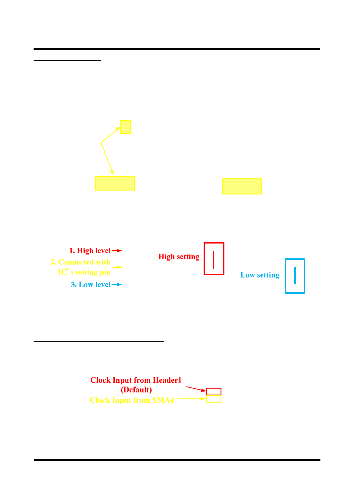
6. Function Setting
Setting pin of each board is shown in yellow area of Figure 9. Pin#2 of each 3HEADER is connected to IC’s
setting pin.
Each setting pin’s high or low setting can set by connecting pin#2 of 3HEADER and high level or low level.
Figure 9 Position of Function Setting Pin
(a)3HEADER Description (b)High Level Setting (c)Low Level Setting
Figure 10 High / Low Setting Description
7. Clock Input from SMA Connector
THEVA213-V3 can also choose the TTL clock input from SMA connector by using 0ohm resistor.
If you want to use SMA connector for clock input, please change the 0ohm resistor mount from R15 to R18.
Figure 11 TTL Clock Input Connector Select
Setting pin
Setting pin

6/13
THAN0186_Rev.1.10_E
Copyright(C) 2015 THine Electronics, Inc. THine Electronics, Inc.
SecurityE
8. Shake Hand Mode
When you use this evaluation kit in “Shake Hand Mode”, Please mount following resistors to connect LOCKN
signal between transmitter and receiver.
*LOCKN signals doesn’t have the connection from / to SMA connector.
Table 4 Resistor Setting for Shake Hand Mode
Connector Eva Board Mount
1mm Pitch Connector Using Case THEVA213-V3 R3
THEVA214-V3 R25
0.5mm Pitch Connector Using Case THEVA213-V3 R10
THEVA214-V3 R47
(a)THEVA213-V3 (Top Side) (b)THEVA214-V3 (Top Side)
Figure 12 LOCKN Connection (1mm Pitch Connector)
(a) THEVA213-V3 (Bottom Side) (b) THEVA214-V3 (Bottom Side)
Figure 13 LOCKN Connection (0.5mm Pitch Connector)
INIT(LOCKN)
Input
R3:Mount(0 )
R25:Mount(0 )
LOCKN Output

7/13
THAN0186_Rev.1.10_E
Copyright(C) 2015 THine Electronics, Inc. THine Electronics, Inc.
SecurityE
9. Dual Display Mode
THEVA213-V3 supports dual display mode.
When you use dual display mode, Please mount following resistors.
Table 5 Resistor Mounting for Dual Display Mode
Connector Mount Unmount
1mm Pitch Connector Using Case R4, R5, R6, R7 R12, R13, R16, R17
0.5mm Pitch Connector Using Case R12, R13, R16, R17 R4, R5, R6, R7
R8, R9, R14, R18
SMA Connector Using Case R8, R9, R12, R13
R14, R16, R17, R18 R4, R5, R6, R7
(a)1mm Pitch Connector (Top Side)
(b)0.5mm Pitch Connector (Bottom Side) (c)SMA Connector (Bottom Side)
Figure 14 Dual Display Mode
10. Status Indicate LED
The following table shows indicating status of each LED.
Table 6 LED Description
THEVA213-V3 THEVA214-V3
D1 3.3V Power Supply Indicator
D2 LOCKN Status Indicator
8/13
THAN0186_Rev.1.10_E
Copyright(C) 2015 THine Electronics, Inc. THine Electronics, Inc.
SecurityE
11. Function
This chapter shows function setting of THEVA213-V3 and THEVA214-V3.
Table 7 THEVA213-V3 Function Setting Description
Silk Symbol Function
EDGE EDGE Input clock triggering edge select.
H: Rising Edge L: Falling Edge
PRBS PRBS
PRBS (Pseudo Random Binary Sequence) generator is active for
evaluation or debugging.
H : PRBS Generator Enable L : Normal Operation
DUAL DUAL
Dual display mode enable.
H: Dual Display Mode (TX1N/P and TX2N/P enabled)
L: Normal Operation (Only TX1N/P enabled, TX2N/P is Hi-Z)
PRE1 PRE1 Pre-Emphasis level se lect input.
PRE1 PRE0 Description
L L w/o Pre-Emphasis
L H 25% Pre-Emphasis
H L 50% Pre-Emphasis
H H 100% Pre-Emphasis
PRE0 PRE0
PDWN PDWN
Power down mode
H: Normal Operation
L: Power Down Mode (TX1N/P and TX2N/P are Hi-Z)
Table 8 THEVA214-V3 Function Setting Description
Silk Symbol Function
EDGE EDGE Input clock triggering edge select.
H: Rising Edge L: Falling Edge
OE OE
Output Enable
H : Output Disable, All Outputs are Hi-Z
L : Output Enable
MOD1 MODE1 Both must be tied to GND.
MODE1 MODE0 Description
L L Normal Mode
Shake Hand Mode
Other Setting Not Available
MOD0 MODE0
PDWN PDWN
Power down mode.
H: Normal Operation
L: Power Down Mode
(All outputs except LOCKN and CLKOUT are held to low)

9/13
THAN0186_Rev.1.10_E
Copyright(C) 2015 THine Electronics, Inc. THine Electronics, Inc.
SecurityE
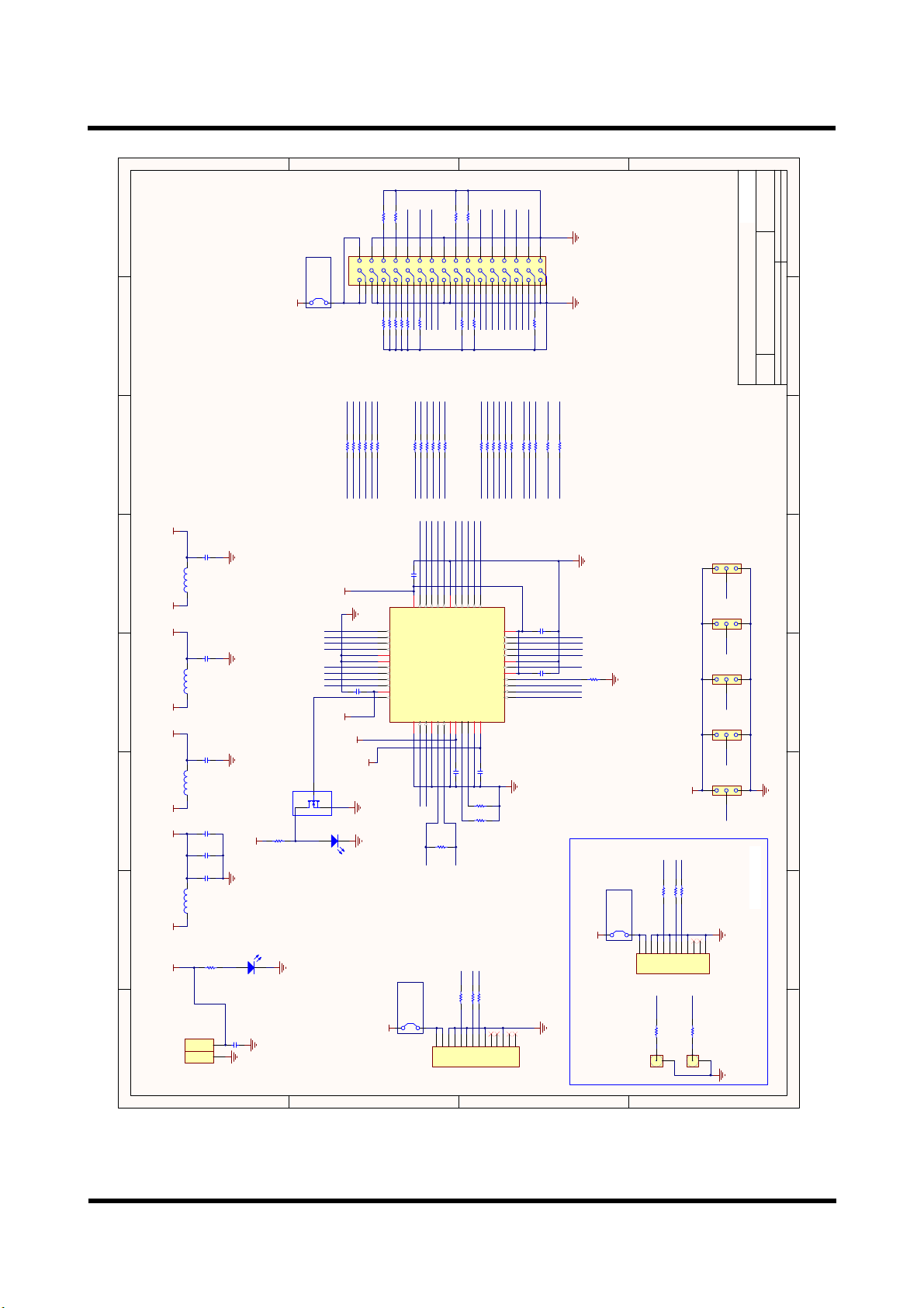
12. Schematic
Figure 15 THEVA213-V3 Schematic
1
1
2
2
3
3
4
4
5
5
6
6
7
7
8
8
D D
C C
B B
A A
Title
Number RevisionSize
A3
Date: 2015/02/26 Sheet of
File: \\..\THCV213.SchDoc Drawn By:
THEVA213-V3
1.00
1 1
0.01uFC11
282836-2(NC)
1
2GND
VCC
CON1
GND 10uF
C6
GND
VDD3.3
SML-310MT
D1
150Ω
R1
GND
VDD3.3
MPZ1608R471A
L1
Inductor
10uF
C1
GND
VDD3.3
MPZ1608R471A
L2
Inductor
0.1uF
C4
GND
G9
B4
B5
B6
B7
B8
B9
R4
R5
R6
R7
R8
R9
G4
G5
G6
G7
G8
EDGE
DE
TX1P
TX1N
1
2
3
3HEAD(NC)
Header2
1
2
3
3HEAD(NC)
Header3
1
2
3
3HEAD(NC)
Header4
1
2
3
3HEAD(NC)
Header5
1
2
3
3HEAD(NC)
Header6
1
2
3
3HEAD(NC)
Header7
GND
EDGE PRBS DUAL PRE1 PRE0 PDWN
PCN10-48P-2.54DSA_LEFT(NC)
1
20
2
3
4
5
6
7
8
9
10
11
12
13
14
15
16
17
18
19
30
29
28
27
26
25
24
23
22
21
40
39
38
37
36
35
34
33
32
31
48
47
46
45
44
43
42
41
Header1
VDD3.3
GND
B4
B5
B6
B7
B8
B9
HSYNC
VSYNC
DE
G9
R4
R5
R6
R7
R8
R9
G4
G5
G6
G7
G8
CLKIN_CONCTRL
INIT
TX1N
GND
52271-1469(NC)
1
2
3
4
5
6
7
8
9
10
11
12
13
14 CON2
0ΩR3
0ΩR4
0ΩR5
VDD3.3
VDD3.3
GND
VDD3.3
1
2
3
4
5
6
7
8
9
10
11
12
CN-FFC(0.5)12PD(NC)
CON3
1
2
SMA103-T16(NC)
SMA4 0Ω(NC)R15
CLKIN_CON 0ΩR11 CLKIN
CLKIN_SMA
GND
1
2
SMA103-T16(NC)
SMA1
GND
1
2
SMA103-T16(NC)
SMA2
VDD LVDSVDD
D14
1
D15
2
D16
3
D17
4
GND
5
CLKIN
6
VDD
7
PRBS
8
DUAL
9
PDWN
10
PRE0
11
PRE1
12
PLLVDD 13
PLLGND 14
TXOUT2+ 15
TXOUT2- 16
LVDSVDD 17
LVDSGND 18
TXOUT1+ 19
TXOUT1- 20
LVDSGND 21
GND 22
EDGE 23
GND 24
INIT 25
VDD 26
SYNC2 27
SYNC1 28
SYNC0 29
DE 30
GND 31
D0 32
D1 33
D2 34
D3 35
VDD 36
D4
37
D5
38
D6
39
D7
40
D8
41
GND
42
D9
43
D10
44
D11
45
D12
46
D13
47
VDD
48
IC1
THCV213
PRBS
PDWN
PRE0
PRE1
HSYNC
VSYNC
CTRL
INIT
0.01uFC9
0.01uFC8
0.01uFC7
0.01uFC10
0.01uFC12
LVDSVDD
PLLVDD
TX2P
TX2N
GND
GND
GND
VDD
TX1P
0ΩR6
0ΩR7TX2P
TX2N
INIT
TX1N
0Ω(NC)R10
TX1P
TX2P
TX2N
INIT_C
TX1N_C
TX1P_C
TX2P_C
TX2N_C
1
2
SMA103-T16(NC)
SMA3
1
2
SMA103-T16(NC)
SMA5
TX1N_C
TX1P_C
TX2P_C
TX2N_C
DUAL
CLKIN
VDD3.3
MPZ1608R471A
L3
Inductor
0.1uF
C5
GND
PLLVDD
0.1uF
C2
0.01uF
C3
Bottom Side
0Ω(NC)R12
0Ω(NC)R13
0Ω(NC)R16
0Ω(NC)R17
0Ω(NC)R8
0Ω(NC)R9
0Ω(NC)R14
0Ω(NC)R18
TX1N_A
TX1P_A
TX2P_A
TX2N_A
0ΩR2
GND
Solder Jumper
W1
Solder Jumper
W2
Solder Jumper
W3
10/13
THAN0186_Rev.1.10_E
Copyright(C) 2015 THine Electronics, Inc. THine Electronics, Inc.
SecurityE
Figure 16 THEVA214-V3 Schematic
1
1
2
2
3
3
4
4
5
5
6
6
7
7
8
8
D D
C C
B B
A A
Title
Number RevisionSize
A3
Date: 2015/02/26 Sheet of
File: \\..\THCV214.SchDoc Drawn By:
THEVA214-V3
1.00
1 1
282836-2(NC)
1
2GND
VCC
CON1
GND 10uF
C7
GND
VDD3.3
SML-310MT
D1
150Ω
R1
GND
VDD3.3
MPZ1608R471A
L1
Inductor
10uF
C1
GND
VDD3.3
MPZ1608R471A
L3
Inductor
0.1uF
C5
GND
B6
B7
B8
B9
DE
RXP
RXN
1
2
3
3HEAD(NC)
Header2
1
2
3
3HEAD(NC)
Header3
1
2
3
3HEAD(NC)
Header4
1
2
3
3HEAD(NC)
Header5
1
2
3
3HEAD(NC)
Header6
GND
EDGE OE MOD1 MOD0 PDWN
52271-1469(NC)
1
2
3
4
5
6
7
8
9
10
11
12
13
14
CON2
0ΩR25
0ΩR28
0ΩR30
VDD3.3
VDD3.3
GND
VDD3.3
1
2
3
4
5
6
7
8
9
10
11
12
CN-FFC(0.5)12PD(NC)
CON3
GND
VDD LVDSVDD
PDWN
HSYNC
VSYNC
CTRL
0.01uFC9
LVDSVDD
PLLVDD
GND
GND
0Ω(NC)R47LOCKN_C
RXN_C
RXP_C
1
2
SMA103-T16(NC)
SMA1
1
2
SMA103-T16(NC)
SMA2
RXP_C
RXN_C
CLKOUT
VDD3.3
MPZ1608R471A
L4
Inductor
0.1uF
C6
GND
PLLVDD
0.1uF
C2
0.01uF
C3
MOD1
1
MOD0
2
PDWN
3
RESERVED0
4
VDDO
5
CLKOUT
6
GNDO
7
D17
8
D16
9
D15
10
D14
11
VDDO
12
D13 13
D12 14
D11 15
D10 16
D9 17
GNDO 18
D8 19
D7 20
D6 21
D5 22
D4 23
VDDO 24
D3 25
D2 26
D1 27
D0 28
GNDO 29
GND 30
DE 31
SYNC0 32
SYNC1 33
SYNC2 34
VDD 35
LOCKN 36
GND
37
EDGE
38
OE
39
LVDSGND
40
RXIN-
41
RXIN+
42
LVDSGND
43
LVDSVDD
44
RESERVED1
45
RESERVED2
46
PLLGND
47
PLLVDD
48
IC1
THCV214
0.01uFC13
0.01uFC12
0.01uFC10
0.01uFC11
0.01uFC8
EDGE
OE
100Ω
R22
MOD1
MOD0
GND
VDD VDDO
U1
SSM3K16FS
VDD3.3
GND
150Ω
R2
D2
GND
LOCKN
R4
R5
R6
R7
R8
R9
G4
G5
G6
G9
B4
B5
G7
G8
RXP
RXN
LOCKN
GND
RXP
RXN
LOCKN
VDD3.3
MPZ1608R471A
L2
Inductor
0.1uF
C4
GND
VDDO
PCN10-48P-2.54DSA_RIGHT(NC)
1
20
2
3
4
5
6
7
8
9
10
11
12
13
14
15
16
17
18
19
30
29
28
27
26
25
24
23
22
21
40
39
38
37
36
35
34
33
32
31
48
47
46
45
44
43
42
41
Header1
VSYNC_C
DE_C
G9_C
R4_C
R5_C
R6_C
R7_C
R8_C
R9_C
G4_C
G5_C
G6_C
G7_C
G8_C
CLKOUT_C
B4_C
B5_C
B6_C
B7_C
B8_C
B9_C
HSYNC_C
CTRL_C
GND GND
VDD3.3
VSYNC
R4
R6
R8
G4
G6
G8
B4
B5
B6
B7
B8
B9
HSYNC
CTRL
R5
R7
R9
G9
G5
G7
DE
10ΩR3
10ΩR4
10ΩR5
10ΩR6
10ΩR7
10ΩR8
10ΩR16
10ΩR18
10ΩR19
10ΩR20
10ΩR21
10ΩR23
10ΩR33
10ΩR34
10ΩR35
10ΩR36
10ΩR37
10ΩR38
10ΩR39
10ΩR40
10ΩR42
10ΩR43
CLKOUT 10ΩR44
VSYNC_C
R4_C
R6_C
R8_C
G4_C
G6_C
G8_C
B4_C
B5_C
B6_C
B7_C
B8_C
B9_C
HSYNC_C
CTRL_C
R5_C
R7_C
R9_C
G9_C
G5_C
G7_C
DE_C
CLKOUT_C
0Ω
R45
0Ω
R31
0Ω
R32
Bottom Side
0Ω(NC)R48
0Ω(NC)R49
0Ω(NC)R46
0Ω(NC)R50
0Ω(NC) R9
0Ω(NC) R11
0Ω(NC) R12
0Ω(NC) R14
0Ω(NC) R15
0Ω(NC)R10
0Ω(NC)R13
0Ω(NC)R24
0Ω(NC)R27
0Ω(NC) R17
0Ω(NC) R26
0Ω(NC) R29
0Ω(NC) R41
GND
Solder Jumper
W2
Solder Jumper
W3
Solder Jumper
W1
11/13
THAN0186_Rev.1.10_E
Copyright(C) 2015 THine Electronics, Inc. THine Electronics, Inc.
SecurityE
13. Bills of Materials
Table 9 THEVA213-V3 BOM
Table 10 THEVA214-V3 BOM
TYPE Value / Part No. Package SPEC Reference No. Q'ty Note
Capacitor 10uF 2012 16V C1, C6 2
Capacitor 0.1uF 1005 16V C2, C4, C5 3
Capacitor 0.01uF 1005 16V C3, C7, C8, C9, C10, C11, C12 7
Connector 282836-2(NC) 5mm pitch 2pin CON1 1
Connector 52271-1469(NC) 1mm_pitch 14pin CON2 1
Connector CN-FFC(0.5)12PD(NC) 0.5mm_pitch 12pin CON3 1
Connector PCN10-48P-2.54DSA_LEFT(NC) 2.54mm_pitch 48pin Header1 1
Connector SMA103-T16(NC) 1.6mm PCB End Jack SMA1, SMA2, SMA3, SMA4, SMA5 5
Header 3HEAD(NC) 2.54mm_pitch --- Header2, Header3, Header4, Header5, Header6, Header7 6
IC THCV213 TQFP48 --- IC1 1
Inductor MPZ1608R471A 1608 1.2A L1, L2, L3 3
LED SML-310MT 1608 GREEN D1 1
Resistor 150 1005 0.1W R1 1
Resistor 0 1005 1A R2, R3, R4, R5, R6, R7, R11 7
Resistor 0(NC) 1005 1A R8, R9, R10, R12, R13, R14, R15, R16, R17, R18 10
TYPE Value / Part No. Package SPEC Reference No. Q'ty Note
Capacitor 10uF 2012 16V C1, C7 2
Capacitor 0.1uF 1005 16V
C2, C4, C5, C6
4
Capacitor 0.01uF 1005 16V
C3, C8, C9, C10, C11, C12, C13
7
Connector SMA103-T16(NC) 1.6mm PCB End Jack SMA1, SMA2 2
Connector PCN10-48P-2.54DSA_RIGHT(NC) 2.54mm_pitch 48pin Header1 1
Connector CN-FFC(0.5)12PD(NC) 0.5mm_pitch 12pin
CON3
1
Connector 52271-1469(NC) 1mm_pitch 14pin
CON2
1
Connector 282836-2(NC) 5mm_pitch 2pin
CON1
1
Header 3HEAD(NC) 2.54mm_pitch --- Header2, Header3, Header4, Header5, Header6 5
IC SSM3K16FS SSM RON15Ω U1 1
IC THCV214 TQFP48 ---
IC1
1
Inductor MPZ1608R471A 1608 1.2A
L1, L2, L3, L4
4
LED0 SML-310MT 1608 GREEN D1,D2 2
Resistor 150Ω 1005 0.1W R1, R2 2
Resistor 100Ω 1005 0.1W
R22
1
Resistor 10Ω 1005 0.1W R3, R4, R5, R6, R7, R8, R16, R18, R19, R20, R21, R23, R33,
R34, R35, R36, R37, R38, R39, R40, R42, R43, R44 23
Resistor 0Ω(NC) 1005 1A R9, R10, R11, R12, R13, R14, R15, R17, R24, R26, R27, R29,
R41, R46, R47, R48, R49, R50
18
Resistor 0Ω 1005 1A
R25, R28, R30, R31, R32, R45
6

12/13
THAN0186_Rev.1.10_E
Copyright(C) 2015 THine Electronics, Inc. THine Electronics, Inc.
SecurityE
14. Set Items
Table 11 Set Items
TYPE Part No.
DC Connector 282836-2
FFC Connector for V-by-One®Link 52271-1469
FFC 14pin 1mm Pitch for V-by-One®Link 98267-0299
Pin Header ---
It’s possible to mount these parts on this board and use.

13/13
THAN0186_Rev.1.10_E
Copyright(C) 2015 THine Electronics, Inc. THine Electronics, Inc.
SecurityE
15. Notices and Requests
Please kindly read, understand and accept this “Notices and Requests” before using this product.
For the Material:
1. The product specifications described in this material are subject to change without prior notice.
2. The circuit diagrams described in this material are examples of the application which may not always
apply to design of respective customers. THine Electronics, Inc. (“THine”) is not responsible for
possible errors and omissions in this material. Please note if the errors or omissions should be found in
this material, THine may not be able to correct them immediately.
3. This material contains THine’s copyright, know-how or other proprietary. Copying or disclosing of the
contents of this material to any third party without THine’s prior permission is strictly prohibited.
For the Product:
1. This product is solely designed for evaluation purpose, and other purposes including mass production
and distribution are not intended.
2. This product has been solely manufactured for electric design engineers but not for end-users.
3. This product is not radiation-tolerant product.
4. This product is presumed to be used for general electric device, not for applications which require
extremely high-reliability/safety (including medical device concerned with critical care, aerospace
device, or nuclear power control device). Also, when using this product for any device concerned with
control and/or safety of transportation mean, traffic signal device, or other various types of safety
device, such use must be after applying appropriate measures to the product.
5. This product has been designed with the utmost care to accomplish the purpose of evaluation of IC
products manufactured by THine Electronics, Inc., however, THine MAKES NO WARRANTIES OR
REPRESENTATIONS WITH REGARD TO ANY PERFORMANCE OR FUNCTION OF THIS
PRODUCT IN ANY CIRCUMSTANCE.
6. This product has been manufactured with the utmost care in quality control and product reliability,
however, there may be faults or defects with a low but fixed probability, as inevitable phenomenon
concerned with semiconductor manufacturing processes. Therefore, Customers are encouraged to have
sufficiently redundant or error-preventive design applied to the use of the product so as not to have
THine’s product cause any social or public damage. Replacement of the product is only available in
case of obvious defects of mount devices at the point of unpacking the product. Neither replacement
nor failure analysis of the product is available in any other case of defects with the product and/or the
product’s components.
7. Customers are asked, if required, to judge by themselves on whether this product falls under the
category of strategic goods under the Foreign Exchange and Foreign Trade Control Law.
8. Please Note that if infringement of any third party’s industrial ownership should occur by using this
product, THine will be exempted from any responsibility unless it directly relates to the production
process or functions of the product.
9. Developing, designing and manufacturing of Customers’ own products, equipments or system by using
of this product is strictly prohibited in any way.
THine Electronics, Inc.
This manual suits for next models
1
Table of contents
Other THine Motherboard manuals

THine
THine THSCM101 Guide

THine
THine THEVA827 User manual

THine
THine THCV215 User manual

THine
THine THC63LVD1023B User manual

THine
THine THSCM101 Guide

THine
THine THC63LVD1023B User manual

THine
THine THEVA252-SMA-V1 User manual

THine
THine THC63LVD1027 User manual

THine
THine THSB-FMC-01VX1 User manual

THine
THine THCV235 User manual


