THine THCV215 User manual

THEVA215-V2_216-V2_UsersGuide_Rev1.20_E
1/13
Copyright(C) 2019 THine Electronics, Inc.
THine Electronics, Inc.
Security E
THCV215 / THCV216 Evaluation Kit
V-by-One®HS Dual Link Evaluation Board
Parts Number: THEVA215-V2, THEVA216-V2
1. General Description
THEVA215-V2 and THEVA216-V2 are
designed to evaluate THCV215 and THCV216
for transmission video data. Each has one
THCV215 or THCV216. This kit can transmit
video data of “Full-HD / 60Hz / 30bit”and
“HD / 120Hz / 30Bit”.
Table 1 Color Width
Width
Link
LVDS Clock Freq.
18bit
Single/Dual
20MHz to 100MHz
24bit
Single/Dual
20MHz to 100MHz
32bit
Single/Dual
20MHz to 85MHz
40bit
Single/Dual
20MHz to 75MHz
2. Features
・Color width selectable : 18/24/32/40 bit
・Single/Dual Link selectable
・Wide Frequency Range
・PLL requires no external components
・V-by-One®HS standard version 1.5 compliant
3. Overview
(a) THEVA215-V2 (Top Side)
(b) THEVA216-V2 (Top Side)
Figure 1 THEVA215-V2 and THEVA216-V2 Top Side View
(a) THEVA215-V2 (Bottom Side) (b) THEVA216-V2 (Bottom Side)
Figure 2 THEVA215-V2 and THEVA216-V2 Bottom Side View

THEVA215-V2_216-V2_UsersGuide_Rev1.20_E
2/13
Copyright(C) 2019 THine Electronics, Inc.
THine Electronics, Inc.
Security E
4. Power Supply Set Up
This chapter shows power supply condition.
Caution: Check if there is no power-GND short on below red trace before supplying any power.
3.3V Power Supply to Each Board
Each evaluation board requires 3.3V power supply. Use “CON1”connector typically.
3.3V Power Supply
Ground
3.3V Power Supply
Ground
(a)THEVA215-V2 (b)THEVA216-V2
Figure 3 Power Supply for Evaluation Board
Power Supply from / to Connector
3.3V power supply can be connected to Header1 and CON2 by using W1, W2 and W3solder jumper.
THEVA215-V2
W1: Connect the 3.3V power supply with pin#1 and 2 of CON2.
W2: Connect the 3.3V power supply with pin#13 and 14 of CON3.
W3: Connect the 3.3V power supply with pin#11 and 12 of CON4.
(a)THEVA215-V2 (Top side) (b) THEVA215-V2 (Bottom side)
Figure 4 THEVA215-V2 Power Supply from / to Each Connector
W1
W2
W3

THEVA215-V2_216-V2_UsersGuide_Rev1.20_E
3/13
Copyright(C) 2019 THine Electronics, Inc.
THine Electronics, Inc.
Security E
THEVA216-V2
W1: Connect the 3.3V power supply with pin#29 and 30 of CON2.
W2: Connect the 3.3V power supply with pin#1 and 2 of CON3.
Figure 5 THEVA216-V2 Power Supply from / to Each Connector
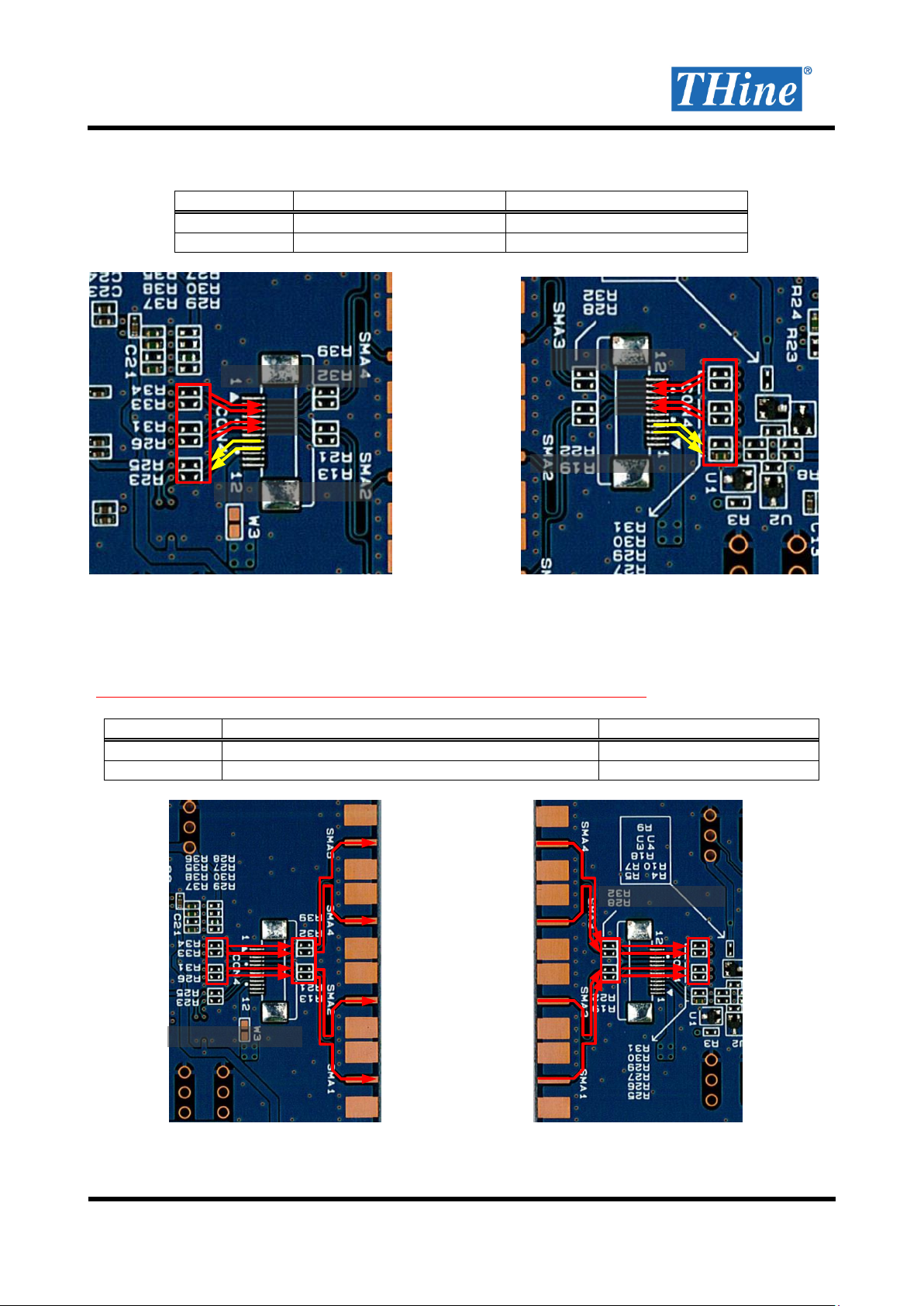
5. V-by-One®HS Input / Output Connector Select
V-by-One®HS input / output connector can be selected by using 0ohm resistors.
(1) 1mm Pitch Connector (Default Setting)
Mount / unmount following 0ohm resistors to use 1mm pitch connector.
Table 2
Mount
Unmount
THEVA215-V2
R7, R8, R9, R10, R11, R12
R23, R25, R26, R31, R33, R34
THEVA216-V2
R12, R13, R14, R15, R16, R17
R25, R26, R27, R29, R30, R31
(a)THEVA215-V2 (Top side) (b)THEVA216-V2 (Top side)
Figure 6 Resistor Mounting for 1mm Pitch Connector
W1
W2
V-by-One®HS output
HTPDN/LOCKN input
TX0
TX1
V-by-One®HS input
HTPDN/LOCKN output
RX0
RX1
THEVA215-V2_216-V2_UsersGuide_Rev1.20_E
4/13
Copyright(C) 2019 THine Electronics, Inc.
THine Electronics, Inc.
Security E
(2) 0.5mm Pitch Connector
Mount / unmount following 0ohm resistors to use 0.5mm pitch connector.
Table 3
Mount
Unmount
THEVA215-V2
R23, R25, R26, R31, R33, R34
R7, R8, R9, R10, R11, R12
THEVA216-V2
R25, R26, R27, R29, R30, R31
R12, R13, R14, R15, R16, R17
(a)THEVA215-V2 (Bottom side) (b)THEVA216-V2 (Bottom side)
Figure 7 Resistor Mounting for 0.5mm Pitch Connector
(3) SMAConnector
Mount / unmount following 0ohm resistors to use SMA connector.
*HTPDN and LOCKN signals don’t have SMA connector input / output connection.
Table 4
Mount
Unmount
THEVA215-V2
R26, R31, R33, R34, R23, R25, R26, R31, R33, R34
R7, R8, R9, R10, R11, R12
THEVA216-V2
R27, R29, R30, R31, R25, R26, R27, R29, R30, R31
R12, R13, R14, R15, R16, R17
(a)THEVA215-V2 (Bottom side) (b)THEVA216-V2 (Bottom side)
Figure 8 Resistor Mounting for SMA Connector
V-by-One®HS output
HTPDN/LOCKN input
TX0
TX1
V-by-One®HS input
HTPDN/LOCKN output
RX0
RX1
V-by-One®HS output
V-by-One®HS input
THEVA215-V2_216-V2_UsersGuide_Rev1.20_E
5/13
Copyright(C) 2019 THine Electronics, Inc.
THine Electronics, Inc.
Security E
6. Function Setting
Setting pin of each board is shown in yellow area of figure9. Pin#2 of each 3HEADER is connected to IC’s
setting pin.
Each setting pin’s high or low setting can set by connecting pin#2 of 3HEADER and high level or low level.
Figure 9 Position of Function Setting Pin
(a)3HEADER Description (b)High Level Setting (c)Low Level Setting
Figure 10 High / Low Setting Description
7. Clock Input from SMA Connector
THEVA215-V2 can also choose the TTL clock input from SMA connector, and it will be converted to LVDS
clock signal by LVDS Buffer IC(SN65LVDS105S). If you want to use SMA connector for clock input,
mount the IC and resistor as below. Table 5
Figure 11 TTL Clock Input Connector Select
Setting pin
Setting pin
Connected with
IC’s setting pin
High side
Low side
High setting
Low setting
Clock input from SMA3
R14
10kohm
R15
0ohm
R16
10kohm
R17
0ohm
R18
10kohm
R19
0ohm
R20
0ohm
R22
0ohm
R24
10kohm

THEVA215-V2_216-V2_UsersGuide_Rev1.20_E
6/13
Copyright(C) 2019 THine Electronics, Inc.
THine Electronics, Inc.
Security E
8. Status Indicate LED
The following table shows indicating status of each LED.
Table 6
THEVA215-V2
THEVA216-V2
D1
3.3V Power Supply Indicator
D2
LOCKN Status Indicator
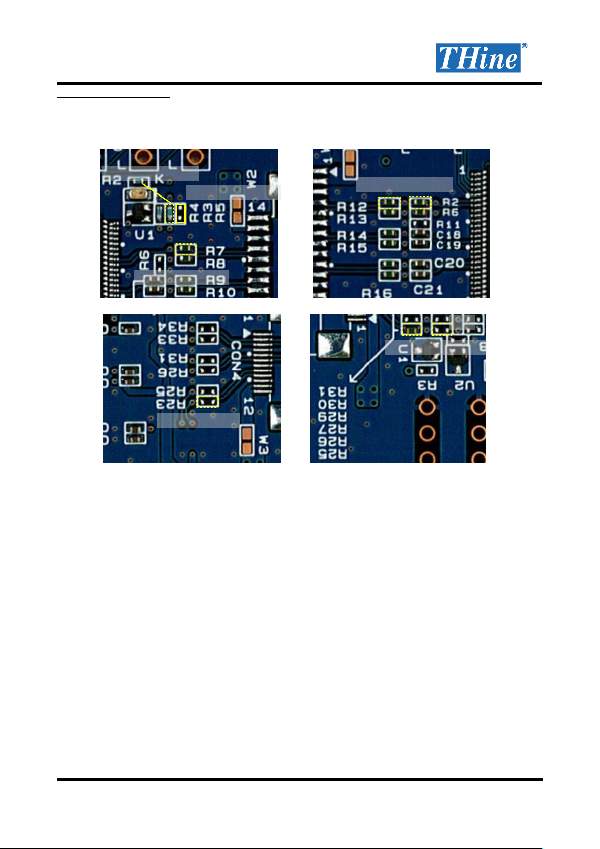
9. LOCKN Sharing , HTPDN Omission and Level Shift
LOCK sharing
LOCKN connection can be shared with V-by-One®HS trace. When you share the LOCKN signal, mount 1k
ohm resistors to share the LOCKN signal, and unmount the 0ohm resistors shown in Figure 12.
(a)THEVA215-V2 (Top Side) (b)THEVA216-V2 (Top Side)
(c) THEVA215-V2 (Bottom Side) (d) THEVA216-V2 (Bottom Side)
Figure 12 LOCKN Sharing
TXN
LOCKN
R6:Mount(1kΩ)R8:Unmount
LOCKN
RXN
R11:Mount(1kΩ)
R6,13:Unmount
R25:Unmount
R26:Unmount
THEVA215-V2_216-V2_UsersGuide_Rev1.20_E
7/13
Copyright(C) 2019 THine Electronics, Inc.
THine Electronics, Inc.
Security E
HTPDN Signal Omission
HTPDN signal can be omitted by using 1k ohm resistor. When you omit the HTPDN signal, mount 1k ohm
resistors to pull down the HTPDN signal at transmitter side, and unmount the 0ohm resistors shown in Figure
13. When the HTPDN omission using, HTPDN output from receiver side is open connection.
(a)THEVA215-V2 (Top Side) (b)THEVA216-V2 (Top Side)
(c)THEVA215-V2 (Bottom Side) (d)THEVA216-V2 (Bottom Side)
Figure 13 HTPDN Signal Omission
R5:Mount(1kΩ)
R3:Unmount(10kΩ)
R7:Unmount
R2, R12:Unmount
R23:Unmount
R25, 5:Unmount
R5
THEVA215-V2_216-V2_UsersGuide_Rev1.20_E
8/13
Copyright(C) 2019 THine Electronics, Inc.
THine Electronics, Inc.
Security E
10. Function
This chapter shows function setting of THEVA215-V2 and THEVA216-V2.
Table 7 THEVA215-V2 Function Setting Description
Silk
Symbol
Function
PDN
PDN
Power down input.
H: Normal Operation
L: Power Down(CML output High Fix, other Hi-Z)
COL0, 1
COL0,1
Color depth select input
L,L : 6bit
H, L : 8bit
L,H : 10bit
H,H : 12bit
SDSEL
SDSEL
Single/Dual select input
H: Channel0, Channel1 Enable
L: Channel0 Enable, Channel1 Disable
RRE1
PRE1
Pre emphasis level select input
H : 100% L : 0%
RES1
Reserved1
Field BET mode enable input
H : Field BET Mode Enable L : Normal Operation
Table 8 THEVA216-V2 Function Setting Description
Silk
Symbol
Function
COL0, 1
COL0,1
Color depth select input
L,L : 6bit
H, L : 8bit
L,H : 10bit
H,H : 12bit
SDSEL
SDSEL
Single/Dual select input
H: Channel0, Channel1 Enable
L: Channel0 Enable, Channel1 Disable
RS
RS
Direction of RS pin depends on Reserved3.
LVDS swing range select input when Reserved3=L.
H: Normal Swing (350mV typ.)
L: Reduced Swing (200mV typ.)
Field BET output when Reserved3=H, Goes LOW when errors
detected.
PDN
PDN
Power down input.
H: Normal Operation
L: Power Down(CML output High Fix, other Hi-Z)
RES3
Reserved3
Field BET mode enable input
H : Field BET Mode Enable L : Normal Operation
THEVA215-V2_216-V2_UsersGuide_Rev1.20_E
9/13
Copyright(C) 2019 THine Electronics, Inc.
THine Electronics, Inc.
Security E
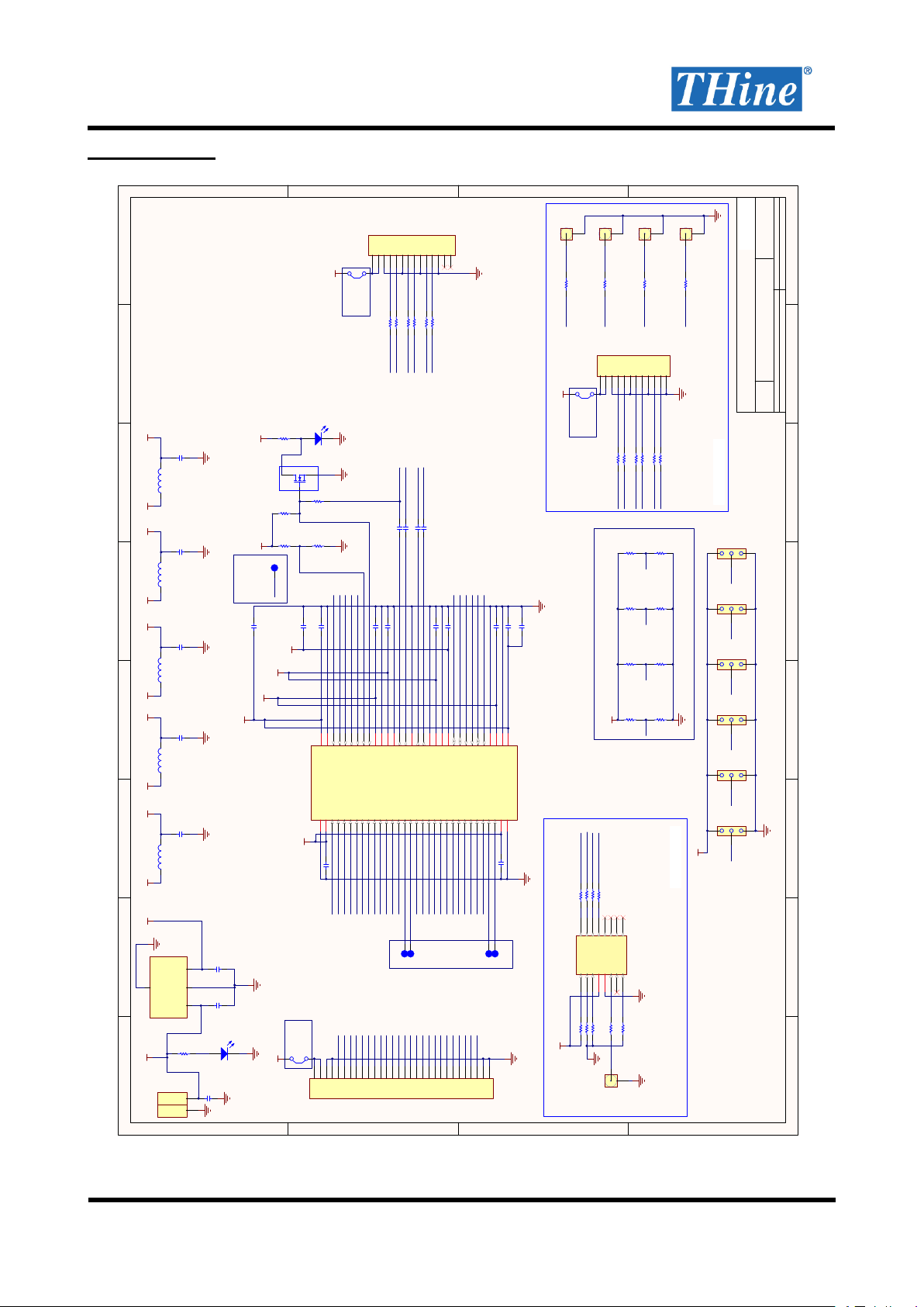
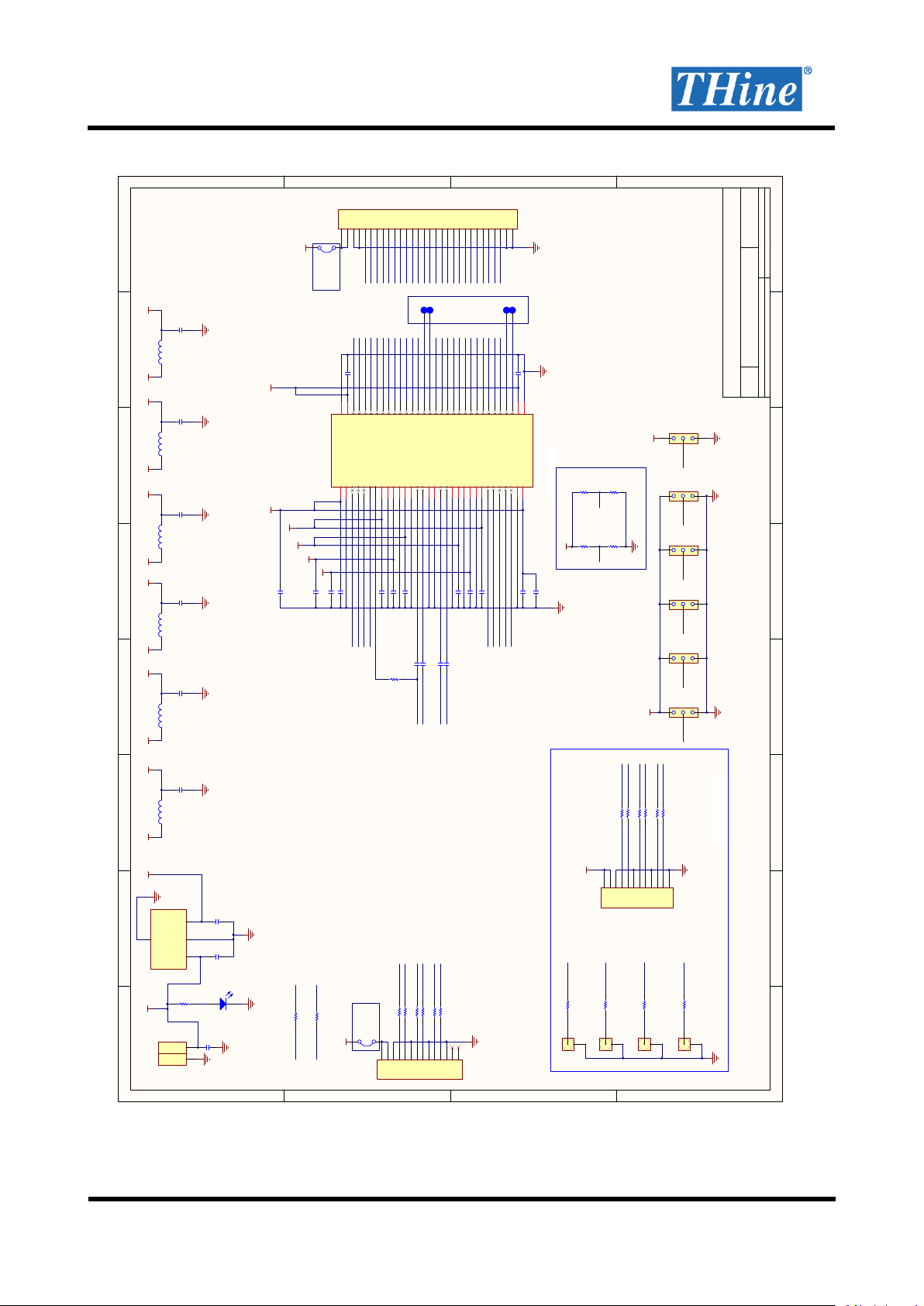
11. Schematic
Figure 14 THEVA215-V2 Schematic
1
1
2
2
3
3
4
4
5
5
6
6
7
7
8
8
D D
C C
B B
A A
Title
Number RevisionSize
A3
Date: 2015/02/26 Sheet of
File: \\..\THCV215.SchDoc Drawn By:
THEVA215-V2
1.00
1 1
1
2
3
3HEAD(NC)
Header1
1
2
3
3HEAD(NC)
Header2
1
2
3
3HEAD(NC)
Header3
1
2
3
3HEAD(NC)
Header4
1
2
3
3HEAD(NC)
Header5
1
2
3
3HEAD(NC)
Header6
GND
SDSEL RES1 COL1 COL0PRE1 PDN
GND
0ΩR7HTPDN
LOCKN
TX0N_C
TX0P_C
GND
52271-1469(NC)
1
2
3
4
5
6
7
8
9
10
11
12
13
14 CON3
0ΩR8
0ΩR9
0ΩR10
VDD3.3
VDD1.8
GND
VDD3.3
1
2
3
4
5
6
7
8
9
10
11
12
CN-FFC(0.5)12PD(NC)
CON4
1
2
SMA103-T16(NC)
SMA1
TX0N_A
TX0P_A
TX1N_C
TX1P_C
0ΩR11
0ΩR12
0Ω(NC)R23HTPDN
LOCKN
TX0N_C
TX0P_C
0Ω(NC)R25
0Ω(NC)R26
0Ω(NC)R31
TX1N_C
TX1P_C
0Ω(NC)R33
0Ω(NC)R34
TX1N_A
TX1P_A
282836-2(NC)
1
2GND
VCC
CON1
GND 10uF
C6
GND
VDD3.3
D1
LED0
150Ω
R1
GND
VDD3.3
MPZ1608R471A
L1
Inductor
10uF
C1
GND
VDD1.8
MPZ1608R471A
L2
Inductor
10uF
C2
GND
VDD3.3
0.1uFC15
0.1uFC16
TX0N_C
TX0P_C
0.1uFC17
0.1uFC18
TX1N_C
TX1P_C
VDL
INPUT
1
GND
2
OUTPUT
3
GND 4
IC1
uPC2918BT
GND
10uF
C7
10uF
C8
GND
VDD1.8 VDD1.8
MPZ1608R471A
L4
Inductor
10uF
C4
GND
CAVDL VDD1.8
MPZ1608R471A
L5
Inductor
10uF
C5
GND
CPVDL
10kΩ
R3 10kΩ
R4
1kΩ(NC)
R5
1kΩ(NC)
R6
GND
U1
SSM3K16FS
GND
51Ω
R2
D2
SML-310MT
GND
GND
LAGND
1
LAVDH
2
TLA0-
3
TLA0+
4
TLB0-
5
TLB0+
6
TLC0-
7
TLC0+
8
TLCLK0-
9
TLCLK0+
10
TLD0-
11
TLD0+
12
TLE0-
13
TLE0+
14
TLF0-
15
TLF0+
16
TLA1-
17
TLA1+
18
TLB1-
19
TLB1+
20
TLC1-
21
TLC1+
22
TLCLK1-
23
TLCLK1+
24
TLD1-
25
TLD1+
26
TLE1-
27
TLE1+
28
TLF1-
29
TLF1+
30
LAVDH
31
LAGND
32
LPVDL 64
LPGND 63
SDSEL 62
COL1 61
COL0 60
RDY 59
PDN 58
HTPDN 57
LOCKN 56
VDL 55
GND 54
CAVDL 53
CAGND 52
TX0n 51
TX0p 50
CAGND 49
TX1n 48
TX1p 47
CAGND 46
CAVDL 45
CPGND 44
CPVDL 43
DRV1 42
DRV0 41
PRE1 40
PRE0 39
Reserved0 38
Reserved1 37
GND 36
VDL 35
LPGND 34
LPVDL 33
IC2
THCV215
52271-3069(NC)
1
2
3
4
5
6
7
8
9
10
11
12
13
14
15
16
17
18
19
20
21
22
23
24
25
26
27
28
29
30
CON2
GND
TLD1N
TLD1P
TLE1N
TLE1P
TLA1N
TLA1P
TLCLK1P
TLB1N
TLB1P
TLC1N
TLC1P
TLCLK1N
TLE0N
TLE0P
TLC0N
TLC0P
TLCLK0N
TLCLK0P
TLD0N
TLD0P
TLA0N
TLA0P
TLB0N
TLB0P
TLD1N
TLD1P
TLE1N
TLE1P
TLA1N
TLA1P
TLCLK1P
TLB1N
TLB1P
TLC1N
TLC1P
TLCLK1N
TLE0N
TLE0P
TLC0N
TLC0P
TLCLK0N
TLCLK0P
TLD0N
TLD0P
TLA0P
TLB0N
TLB0P
TLA0N
0.01uF
C12
LAVDH
GND
0.01uF
C22
TLF0N
TLF0P
TLF1N
TLF1P
RES1
RES0
PRE0
PRE1
DRV0
DRV1
TX1P
TX1N
TX0P
TX0N
HTPDN
PDN
RDY
COL0
COL1
SDSEL
0.01uF
C11
0.01uF
C13
0.01uF
C14
0.01uF
C19
0.01uF
C20
0.01uF
C21
0.01uF
C23
LPVDL
VDL
CAVDL
CPVDL
4.7uF
C10
4.7uF
C9
HTPDN
LOCKN
VDL VDL
LAVDH VDD1.8
MPZ1608R471A
L3
Inductor
10uF
C3
GND
LPVDL
0Ω(NC)
R27
GND
VDD1.8
0Ω(NC)
R28
0Ω(NC)
R29
0Ω(NC)
R38
0Ω
R30
DRV0DRV1RES0PRE0
0Ω
R35
0Ω
R36
0Ω
R37
EN1
1
EN2
2
EN3
3
VCC
4
GND
5
A
6
NC
7
EN4
84Z 9
4Y 10
3Z 11
3Y 12
2Z 13
2Y 14
1Z 15
1Y 16
IC3
SN65LVDS105D(NC)
1
2
SMA103-T16(NC)
SMA3
0Ω(NC)R22
GND
10kΩ(NC)R18
10kΩ(NC)R16
10kΩ(NC)R14
10kΩ(NC)R24
VDD3.3
GND
TLCLK1P
TLCLK1N
TLCLK0N
TLCLK0P
0Ω(NC)R15
0Ω(NC)R17
0Ω(NC)R19
0Ω(NC)R20
LVTTL to LVDS Convert for BET MODE
RDY
TX0N_A
TX0P_A
TX1N_A
TX1P_A
TP1
TP3
TP2
TP5
TP4
Bottom Side
0Ω(NC)R13
0Ω(NC)R21
0Ω(NC)R32
0Ω(NC)R39
1
2
SMA103-T16(NC)
SMA2
1
2
SMA103-T16(NC)
SMA4
1
2
SMA103-T16(NC)
SMA5
GND
4.7uF
C24
Bottom Side
Solder Jumper
W1
Solder Jumper
W2
Solder Jumper
W3
THEVA215-V2_216-V2_UsersGuide_Rev1.20_E
10/13
Copyright(C) 2019 THine Electronics, Inc.
THine Electronics, Inc.
Security E
Figure 15 THEVA216-V2 Schematic
1
1
2
2
3
3
4
4
5
5
6
6
7
7
8
8
D D
C C
B B
A A
Title
Number RevisionSize
A3
Date: 2019/04/04 Sheet of
File: \\..\THCV216_.SchDoc Drawn By:
THEVA216-V2
1.20
1 1
1
2
3
3HEAD(NC)
Header1
1
2
3
3HEAD(NC)
Header2
1
2
3
3HEAD(NC)
Header6
1
2
3
3HEAD(NC)
Header3
1
2
3
3HEAD(NC)
Header4
1
2
3
3HEAD(NC)
Header5
GND
SDSEL RES3 COL1 COL0 RSPDN
GND
0ΩR12 HTPDN_C
LOCKN_C
GND
52271-1469(NC)
1
2
3
4
5
6
7
8
9
10
11
12
13
14
CON3
0ΩR13
0ΩR14
0ΩR15
VDD3.3
VDD1.8
GND
VDD3.3
1
2
3
4
5
6
7
8
9
10
11
12
CN-FFC(0.5)12PD(NC)
CON4
1
2
SMA103-T16(NC)
SMA1
1
2
SMA103-T16(NC)
SMA2
0ΩR16
0ΩR17
0Ω(NC)R25HTPDN_A
LOCKN_A
RX0N_A
RX0P_A
0Ω(NC)R26
0Ω(NC)R27
0Ω(NC)R29
RX1N_A
RX1P_A 0Ω(NC)R30
0Ω(NC)R31
1
2
SMA103-T16(NC)
SMA3
1
2
SMA103-T16(NC)
SMA4
282836-2(NC)
1
2GND
VCC
CON1
GND 10uF
C7
GND
VDD3.3
SML-310MT
D1
150Ω
R1
GND
VDD3.3
MPZ1608R471A
L1
Inductor
10uF
C1
GND
VDD1.8
MPZ1608R471A
L3
Inductor
10uF
C3
GND
0.1uFC18 0.1uFC19
RX0N_C
RX0P_C
0.1uFC20 0.1uFC21
RX1N_C
RX1P_C
VDL
INPUT
1
GND
2
OUTPUT
3
GND 4
IC1
uPC2918BT
GND
10uF
C8 10uF
C9
GND
VDD1.8 VDD1.8
MPZ1608R471A
L5
Inductor
10uF
C5
GND
CPVDL0 VDD1.8
MPZ1608R471A
L6
Inductor
10uF
C6
GND
CPVDL1
1kΩ(NC)
R11
GND
52271-3069(NC)
1
2
3
4
5
6
7
8
9
10
11
12
13
14
15
16
17
18
19
20
21
22
23
24
25
26
27
28
29
30 CON2
RX1P
RX1N
RX0P
RX0N
0.01uF
C13
0.01uFC15
0.01uFC16
0.01uFC17
LPVDH
VDL
CAVDL
CPVDL0
4.7uFC10
LAVDH VDD1.8
MPZ1608R471A
L4
Inductor
10uF
C4
GND
CAVDL
GND
VDD1.8
0Ω(NC)
R20
0Ω(NC)
R21
RES2RES1
0Ω
R23
0Ω
R24
LPVDH
1
LPGND
2
SDSEL
3
COL1
4
COL0
5
HTPDN
6
LOCKN
7
VDL
8
GND
9
CPVDL0
10
CPGND0
11
CAVDL
12
CAGND
13
RX0n
14
RX0p
15
CAGND
16
CAGND
17
RX1n
18
RX1p
19
CAGND
20
CAVDL
21
CPGND1
22
CPVDL1
23
GND
24
VDL
25
Reserved1
26
PDN
27
Reserved2
28
Reserved3
29
RS
30
LPGND
31
LPVDH
32
LAGND 64
LAVDH 63
RLA0- 62
RLA0+ 61
RLB0- 60
RLB0+ 59
RLC0- 58
RLC0+ 57
RLCLK0- 56
RLCLK0+ 55
RLD0- 54
RLD0+ 53
RLE0- 52
RLE0+ 51
RLF0- 50
RLF0+ 49
RLA1- 48
RLA1+ 47
RLB1- 46
RLB1+ 45
RLC1- 44
RLC1+ 43
RLCLK1- 42
RLCLK1+ 41
RLD1- 40
RLD1+ 39
RLE1- 38
RLE1+ 37
RLF1- 36
RLF1+ 35
LAVDH 34
LAGND 33
IC2
THCV216
RES1
RES2
HTPDN
COL1
RS
PDN
RES3
LOCKN
COL0
SDSEL
RLCLK0P
RLD0P
RLE0P
RLF0P
RLA1P
RLB1P
RLC1P
RLCLK1P
RLD1P
RLE1P
RLC0P
RLB0P
RLA0P
RLF1P
RLD0N
RLE0N
RLF0N
RLA1N
RLB1N
RLC1N
RLCLK1N
RLD1N
RLE1N
RLF1N
RLCLK0N
RLC0N
RLB0N
RLA0N
0.01uFC22
0.01uFC23
0.01uFC24
0.01uFC26
CPVDL1
4.7uFC11
4.7uFC12
0.01uFC14
0.01uFC25
GND
LAVDH
RLCLK0P
RLD0P
RLC0P
RLB0P
RLA0P
RLD0N
RLE0N
RLCLK0N
RLC0N
RLB0N
RLA0N
RLA1P
RLB1P
RLC1P
RLCLK1P
RLD1P
RLE1P
RLA1N
RLB1N
RLC1N
RLCLK1N
RLD1N
RLE1N
VDD3.3
GND
RX0N_C
RX0P_C
RX1N_C
RX1P_C
GND
RX0N_A
RX0P_A
RX1N_A
RX1P_A
HTPDN_C
LOCKN_C
RX0N_C
RX0P_C
RX1N_C
RX1P_C
VDD3.3
MPZ1608R471A
L2
Inductor
10uF
C2
GND
LPVDH
RLE0P
TP3
TP4
TP1
TP2
Bottom Side
0Ω(NC)R19
0Ω(NC)R22
0Ω(NC)R28
0Ω(NC)R32
0ΩR2
0ΩR6
HTPDN
LOCKN
HTPDN_C
LOCKN_C
4.7uFC27
Solder Jumper
W2
Solder Jumper
W1
Bottom Side
GND
VDD3.3
THEVA215-V2_216-V2_UsersGuide_Rev1.20_E
11/13
Copyright(C) 2019 THine Electronics, Inc.
THine Electronics, Inc.
Security E
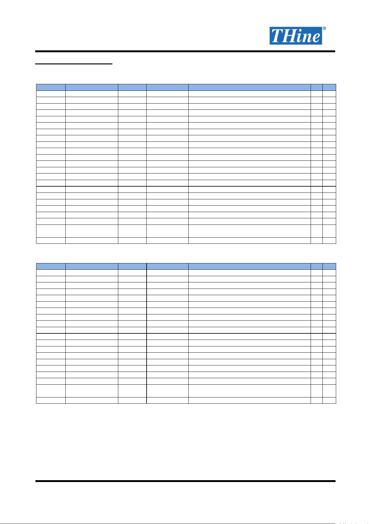
12. Bills of Materials
Table 9 THEVA215-V2 BOM
Table 10 THEVA216-V2 BOM
TYPE Value / Part No. Package SPEC Reference No. Q'ty Note
Capacitor 10uF 2012 16V
C1, C2, C3, C4, C5, C6, C7, C8 8
Capacitor 4.7uF 1005 16V
C9, C10, C24 3
Capacitor 0.01uF 1005 16V
C11, C12, C13, C14, C19, C20, C21, C22, C23 9
Capacitor 0.1uF 1005 16V
C15, C16, C17, C18 4
Connector 282836-2(NC) 5mm_pitch 2pin
CON1 1
Connector 52271-3069(NC) 1mm_pitch 30pin
CON2 1
Connector 52271-1469(NC) 1mm_pitch 14pin
CON3 1
Connector CN-FFC(0.5)12PD(NC) 0.5mm_pitch 12pin
CON4 1
Connector SMA103-T16(NC) 1.6mm PCB End Jack
SMA1, SMA2, SMA3, SMA4, SMA5 5
Header 3HEAD(NC) 2.54mm_pitch ---
Header1, Header2, Header3, Header4, Header5, Header6 6
IC uPC2918BT SC-63 1A
IC1 1
IC THCV215 TSSOP64 ---
IC2 1
IC SN65LVDS105D(NC) TSSOP 4V
IC3 1
IC SSM3K16FS SSM RON15Ω
U1 1
Inductor MPZ1608R471A 1608 1.2A
L1, L2, L3, L4, L5 5
LED0 SML-310MT 1608 GREEN
D1,D2 1
Resistor 51Ω 1005 0.1W
R2 1
Resistor 150Ω 1005 0.1W
R1 1
Resistor 10kΩ 1005 0.1W
R3, R4 3
Resistor 1kΩ(NC) 1005 0.1W
R5, R6 2
Resistor 0Ω 1005 1A
R7, R8, R9, R10, R11, R12, R30, R35, R36, R37 10
Resistor 0Ω(NC) 1005 1A
R13, R15, R17, R19, R20, R21, R22, R23, R25, R26, R27, R28,
R29, R31, R32, R33, R34, R38, R39
19
Resistor 10kΩ(NC) 1005 0.1W
R14, R16, R18, R24 4
TYPE Value / Part No. Package SPEC Reference No. Q'ty Note
Capacitor 10uF 2012 16V
C1, C2, C3, C4, C5, C6, C7, C8, C9 9
Capacitor 4.7uF 1005 16V
C10, C11, C12, C27 4
Capacitor 0.01uF 1005 16V
C13, C14, C15, C16, C17, C22, C23, C24, C25, C26 10
Capacitor 0.1uF 1005 16V
C18, C19, C20, C21 4
Connector 282836-2(NC) 5mm_pitch 2pin
CON1 1
Connector 52271-3069(NC) 1mm_pitch 30pin
CON2 1
Connector 52271-1469(NC) 1mm_pitch 14pin
CON3 1
Connector CN-FFC(0.5)12PD(NC) 0.5mm_pitch 12pin
CON4 1
Connector SMA103-T16(NC) 1.6mm PCB End Jack
SMA1, SMA2, SMA3, SMA4 4
Header 3HEAD(NC) 2.54mm_pitch ---
Header1, Header2, Header3, Header4, Header5, Header6 6
IC uPC2918BT SC-63 1A
IC1 1
IC THCV216 TSSOP64 ---
IC2 1
IC SSM3K16FS SSM RON15Ω
U1, U2, U3, U4 4
Inductor MPZ1608R471A 1608 1.2A
L1, L2, L3, L4, L5, L6 6
LED0 SML-310MT 1608 GREEN
D1 1
Resistor 150Ω 1005 0.1W
R1 1
Resistor 0Ω 1005 1A
R2, R6, R12, R13, R14, R15, R16, R17, R23,R24, R25 10
Resistor 10kΩ(NC) 1005 0.1W
R3, R4, R9, R10 4
Resistor 0Ω(NC) 1005 1A
R5, R7, R8, R18, R19, R20, R21, R22, R26, R27, R28, R29, R30,
R31, R32
16
Resistor 1kΩ(NC) 1005 0.1W
R11 1

THEVA215-V2_216-V2_UsersGuide_Rev1.20_E
12/13
Copyright(C) 2019 THine Electronics, Inc.
THine Electronics, Inc.
Security E
13. Set Items Table 11 Set Items
TYPE
Part No.
DC Connector
282836-2
FFC Connector for V-by-One®HS Link
52271-1469
FFC 14pin 1mm pitch for V-by-One®HS Link
98267-0299
Pin Header
---
It's possible to mount these parts on this board and use.

THEVA215-V2_216-V2_UsersGuide_Rev1.20_E
13/13
Copyright(C) 2019 THine Electronics, Inc.
THine Electronics, Inc.
Security E
14. Notices and Requests
Please kindly read, understand and accept this “Notices and Requests” before using this product.
For the Material:
1. The product specifications described in this material are subject to change without prior notice.
2. The circuit diagrams described in this material are examples of the application which may not always
apply to design of respective customers. THine Electronics, Inc. (“THine”) is not responsible for
possible errors and omissions in this material. Please note if the errors or omissions should be found in
this material, THine may not be able to correct them immediately.
3. This material contains THine’s copyright, know-how or other proprietary. Copying or disclosing of the
contents of this material to any third party without THine’s prior permission is strictly prohibited.
For the Product:
1. This product is solely designed for evaluation purpose, and other purposes including mass production
and distribution are not intended.
2. This product has been solely manufactured for electric design engineers but not for end-users.
3. This product is not radiation-tolerant product.
4. This product is presumed to be used for general electric device, not for applications which require
extremely high-reliability/safety (including medical device concerned with critical care, aerospace
device, or nuclear power control device). Also, when using this product for any device concerned with
control and/or safety of transportation mean, traffic signal device, or other various types of safety
device, such use must be after applying appropriate measures to the product.
5. This product has been designed with the utmost care to accomplish the purpose of evaluation of IC
products manufactured by THine Electronics, Inc., however, THine MAKES NO WARRANTIES OR
REPRESENTATIONS WITH REGARD TO ANY PERFORMANCE OR FUNCTION OF THIS
PRODUCT IN ANY CIRCUMSTANCE.
6. This product has been manufactured with the utmost care in quality control and product reliability,
however, there may be faults or defects with a low but fixed probability, as inevitable phenomenon
concerned with semiconductor manufacturing processes. Therefore, Customers are encouraged to have
sufficiently redundant or error-preventive design applied to the use of the product so as not to have
THine’s product cause any social or public damage. Replacement of the product is only available in
case of obvious defects of mount devices at the point of unpacking the product. Neither replacement
nor failure analysis of the product is available in any other case of defects with the product and/or the
product’s components.
7. Customers are asked, if required, to judge by themselves on whether this product falls under the
category of strategic goods under the Foreign Exchange and Foreign Trade Control Law.
8. Please Note that if infringement of any third party’s industrial ownership should occur by using this
product, THine will be exempted from any responsibility unless it directly relates to the production
process or functions of the product.
9. Developing, designing and manufacturing of Customers’own products, equipments or system by using
of this product is strictly prohibited in any way.
THine Electronics, Inc.
This manual suits for next models
4
Table of contents
Other THine Motherboard manuals

THine
THine THC63LVD1023B User manual

THine
THine THSB-FMC-01VX1 User manual

THine
THine THC63LVD1023B User manual

THine
THine THC63LVDM83D User manual

THine
THine THC63LVDM83D User manual

THine
THine THSCM101 Guide

THine
THine THEVA213-V3 User manual

THine
THine THSCM101 Guide

THine
THine THC63LVD1027D User manual

THine
THine THCV235 User manual


Popular Motherboard manuals by other brands


mikroElektronika
mikroElektronika Click Board I2C isolator click quick start guide

Xilinx
Xilinx Platform Cable USB II manual

Commell
Commell LV-67A user manual

ASROCK
ASROCK Q1900B-ITX Instruction

Advantech
Advantech PCI-7020F PCI-7020VG PCI-7020LV PCI-7020 user manual

Biostar
Biostar Hi-Fi Z87S 3D Setup manual