TMC AI5VG+ User manual

AI5VG+
Pentium MVP3
Baby AT Motherboard
User’s Manual
Version 1.0F


Contents
AI5VG+ User’s Manual i
Contents
Chapter 1 Introduction....................................................1
Chapter 2 Specifications..................................................2
Chapter 3 Hardware Description ...................................5
3.1 Processor and CPU Voltage ..............................................7
3.2 L2 Cache Memory.............................................................7
3.3 Main Memory....................................................................7
3.4 BIOS..................................................................................9
3.5 Onboard PCI EIDE..........................................................10
3.6 Onboard Multi-I/O...........................................................10
3.7 Onboard CPU Temperature Sensor.................................10
3.8 I/O Port Address Map......................................................11
3.9 DMA Channels................................................................11
3.10 Interrupt Request Lines (IRQ).......................................12
3.11 Accelerated Graphics Port (AGP) Slot..........................12
Chapter 4 Hardware Settings........................................13
4.1 SW1(1-8): CPU Frequency Selector ...............................15
4.2 JP1, SW1(4): DRAM Operating Frequency ........................20
4.3 JP6: System Frequency Divider ......................................20
4.4 SW2(1-4): CPU Voltage Selector ...................................20
4.5 JP2: Clear CMOS Selection ............................................22
Chapter 5 Installation....................................................23
5.1 I/O Connectors.................................................................25
5.2 J8: AT Power Supply Connector.....................................25
5.3 J7: ATX Power Supply Connector..................................26
5.4 J3, J4: AT Keyboard and PS/2 Mouse Connectors.........26
5.5 J6, J5: Serial Ports...........................................................27
5.6 J11: Floppy Drive Connector ..........................................27
5.7 J10, J12: EIDE Connectors..............................................28
5.8 J9: Parallel Port Connector..............................................29
5.9 J15: IrDA Connector .......................................................29
5.10 J1: USB Connector........................................................29

Contents
ii AI5VG+ User’s Manual
5.11 J13 Wake on LAN Connector .......................................30
5.12 J14: CPU Fan Power Connector....................................30
5.13 J20 Front Bezel Connector............................................30
Chapter 6 BIOS Configuration.....................................33
6.1 BIOS Introduction ...........................................................34
6.2 BIOS Setup......................................................................34
6.3 Standard CMOS Setup.....................................................36
6.4 BIOS Features Setup .......................................................39
6.5 Chipset Features Setup....................................................42
6.6 Power Management Setup...............................................44
6.7 PNP/PCI Configuration...................................................47
6.8 Load BIOS Defaults ........................................................50
6.9 Load Setup Defaults ........................................................50
6.10 Integrated Peripherals....................................................51
6.11 Supervisor / User Password...........................................53
6.12 IDE HDD Auto Detection .............................................54
6.13 HDD Low Level Format................................................54
6.14 Save & Exit Setup..........................................................55
6.15 Exit Without Saving......................................................55

Chapter 1 Introduction
AI5VG+ User’s Manual 1
Chapter 1 Introduction
This manual is designed to give you information on the AI5VG+
Motherboard. It is divided into the following six sections:
•
••
•
Introduction
•
••
•
Specifications
•
••
•
Hardware Description
•
••
•
Hardware Settings
•
••
•
Installation
•
••
•
BIOS Configuration
Checklist
Please check that your package is complete and contains the items below.
If you discover damaged or missing items, please contact your dealer.
The AI5VG+ Motherboard
This user’s manual
1 IDE ribbon cable
1 floppy ribbon cable
2 serial ribbon cables*
1 parallel ribbon cable
1 PS/2 cable
1 diskette containing Bus Master IDE drivers and flash utility
and 1 diskette containing VxD drivers or 1 CD containing
drivers and utilities
* Use the two serial ribbon cables provided to avoid compatibility
problems.

Chapter 2 Specifications
2 AI5VG+ User’s Manual
Chapter 2 Specifications
Based on VIA’s MVP3 chipset, the AI5VG+ is a Baby AT Pentium
motherboard that supports all the features to make a Microsoft PC’97
compliant PCI/ISA system.
The AI5VG+ comes with an Accelerated Graphics Port (AGP) slot,
power management functionality that is compliant with ACPI and
legacyAPM requirements. Inaddition to standard PIO and DMA mode
operation, it features Ultra DMA/33 for improved disk I/O throughput.
The main features of this motherboard are listed as follows:
Main Processor
Intel Pentium 100/133/166/200
Intel Pentium MMX (P55C) 166/200/233
Cyrix 6x86/6x86L P166+/P200+
Cyrix 6x86MX PR166/PR200/PR233/PR266
Cyrix 6x86MII 266/PR300/PR333/PR366
AMD K5 PR100/PR133/PR166
AMD K6 166/200/233/266/300
AMD K6-2/300/333/350/366/380/400/450
IDT WinChip C6 180/200/225MHz
IDT WinChip2-3D 200/225/266MHz
L2 Cache
512KB Pipelined Burst Synchronous SRAM onboard
Main Memory
Two 72-pin SIMM sockets and three 168-pin DIMM sockets
Memory Type
SIMMs: FPM (Fast Page Mode) or EDO (Extended Data Out)
SIMM Size: 4MB, 8MB, 16MB, 32MB, 64MB
DIMMs: EDO DRAM or SDRAM (Synchronous DRAM)
DIMM Size: 8MB, 16MB, 32MB, 64MB, 128MB
Chipset
VIA’s MVP3 chipset with built-in PCI EIDE

Chapter 2 Specifications
AI5VG+ User’s Manual 3
Onboard I/O
Winbond W83877 for two serial, one parallel, one floppy drive
interface and IrDA support
Onboard Bus Mastering EIDE
Two EIDE interfaces for up to four devices, support PIO Mode 3/4
or Ultra DMA/33 IDE Hard Disk and ATAPI CD-ROM.
BIOS
Licensed BIOS with additional features:
• FLASH EEPROM (128KB) for BIOS update
• ISA Plug and Play (PnP) extension
• Power management
CPU Temperature Sensor
The AD22105 IC onthe motherboard is a temperature sensor for the
CPU. When the CPU temperature exceeds threshold value, the CPU
slows down automatically to allow it to cool down to a safe level.
Windows 95 Shut-Down
This allows the PC to power off via Windows 95 operating system.
(This feature requires ATX power supply.)
AGP Support (Accelerated Graphics Port)
The AI5VG+ motherboard comes with an AGP slot for an AGP
VGA card that supports 133MHz 2X mode for AD and SBA
signaling.
PC97 Compliance
The AI5VG+ implements BIOS and hardware designs that meet
PC97 standards and is fully compatible with all Windows operating
systems.
Expansion Slots
Four 32-bit PCI slots
Two 16-bit ISA slots
One AGP slot
Form Factor
Baby AT, 9”x 8.6” (23cm x 22cm)

Chapter 2 Specifications
4 AI5VG+ User’s Manual
This page is intentionally left blank.

Chapter 3 Hardware Description
AI5VG+ User’s Manual 5
Chapter 3 Hardware Description
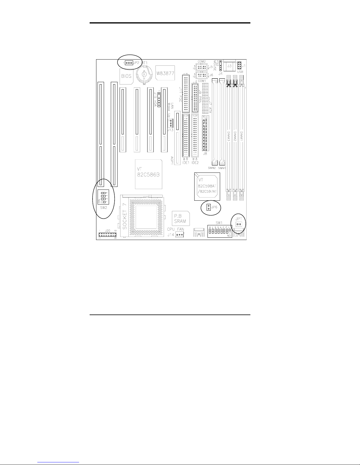
This chapter briefly describes each of the major features of the AI5VG+
motherboard. The layout of the board is shown in Figure 1 which shows
the locations of the key components. The topics covered in this chapter
are as follows:
3.1 Processor and CPU Voltage........................................................7
3.2 L2 Cache Memory.......................................................................7
3.3 Main Memory..............................................................................7
3.4 BIOS ...........................................................................................9
3.5 Onboard PCI EIDE...................................................................10
3.6 Onboard Multi-I/O....................................................................10
3.7 Onboard CPU Temperature Sensor...........................................10
3.8 I/O Port Address Map...............................................................11
3.9 DMA Channels..........................................................................11
3.10 Interrupt Request Lines (IRQ).................................................12
3.11 Accelerated Graphics Port (AGP) Slot....................................12
Chapter 3 Hardware Description
6 AI5VG+ User’s Manual
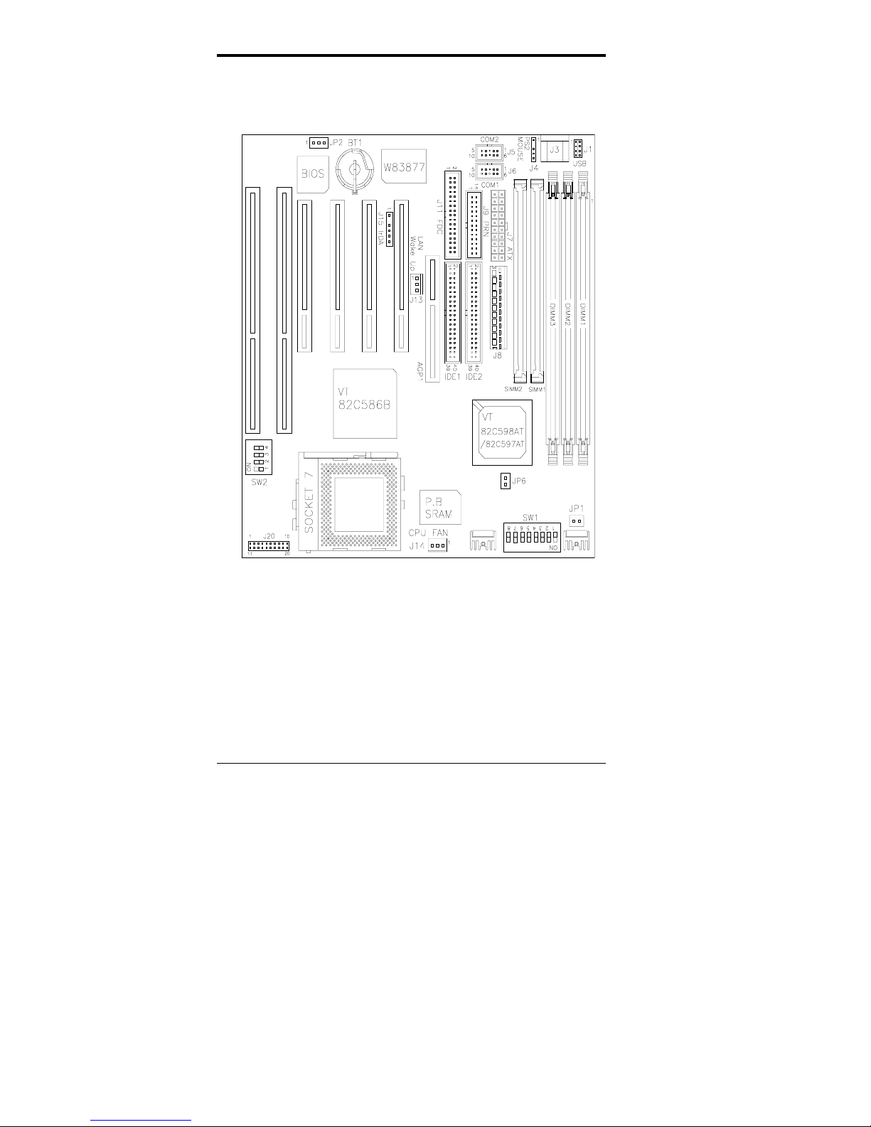
Figure 1: Layout of the AI5VG+ Motherboard

Chapter 3 Hardware Description
AI5VG+ User’s Manual 7
3.1 Processor and CPU Voltage
The AI5VG+ is designed to take a Pentium Processor with a bus speed of
60, 66, 75, 83 and 100 MHz. The internal clock of the CPU can be
multiples of 1.5, 2, 2.5, 3, 3.5, 4 and 4.5 of the bus clock, the CPU
frequency can be 90 to 300MHz.
The onboard CPU voltage regulator provides support for CPUs Vcore
which require voltage other than 3.3V such as 2.8V, and/or power
consumption higher than 10 watts.
3.2 L2 Cache Memory
The AI5VG+ supports 512KB P.B. (Pipelined Burst) Synchronous
Cache. The P.B. Synchronous Cache boosts the system’s performance,
10% higher than regular Asynchronous Cache.
3.3 Main Memory
The AI5VG+ motherboard supports two 72-pin SIMMs and three
168-pin DIMMs (Dual In-line Memory Module) sockets. The DRAMs
for the SIMM sockets can be 4MB, 8MB, 16MB, 32MB, and 64MB in
EDO and FPM types. DIMM modules can be 8MB, 16MB, 32MB,
64MB and 128MB in EDO DRAM or SDRAM type.
The following should be noted when populating the SIMM/DIMM
sockets:
1. Each bank**should consist of the same size SIMMs.
2. Each bank should consist of the same type SIMMs. For example,
SIMM1 and SIMM2 are both be EDO or Page Mode.
3. Each bank consists of two SIMM slots or one DIMM slot. For
example, SIMM 1 and SIMM 2 are considered as one bank and
DIMM 1 as another one.
Chapter 3 Hardware Description
8 AI5VG+ User’s Manual
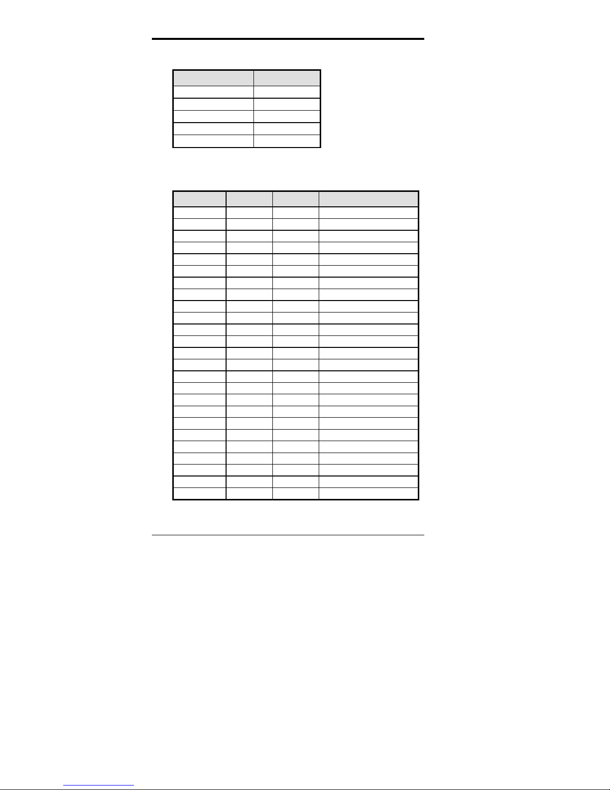
(1) 72-pin SIMM (5V) - EDO DRAM
SIMM1, SIMM2 Total Memory
4MB×2 8MB
8MB×2 16MB
16MB×2 32MB
32MB×2 64MB
64MB×2 128MB
(2) 168-pin DIMM (3.3V) - SDRAM or EDO DRAM
DIMM3 DIMM2 DIMM1 Total Memory
8MB ----- ----- 8MB
16MB ----- ----- 16MB
32MB ----- ----- 32MB
64MB ----- ----- 64MB
128MB ----- ----- 128MB
8MB 8MB ----- 16MB
16MB 8MB ----- 24MB
32MB 8MB ----- 40MB
64MB 8MB ----- 72MB
128MB 8MB ----- 136MB
8MB 8MB 8MB 24MB
16MB 8MB 8MB 32MB
32MB 8MB 8MB 48MB
64MB 8MB 8MB 80MB
128MB 8MB 8MB 144MB
16MB 16MB ----- 32MB
32MB 16MB ----- 48MB
64MB 16MB ----- 80MB
128MB 16MB ----- 144MB
16MB 16MB 8MB 40MB
32MB 16MB 8MB 56MB
64MB 16MB 8MB 88MB
128MB 16MB 8MB 152MB
16MB 16MB 16MB 48MB
32MB 16MB 16MB 64MB
Chapter 3 Hardware Description
AI5VG+ User’s Manual 9
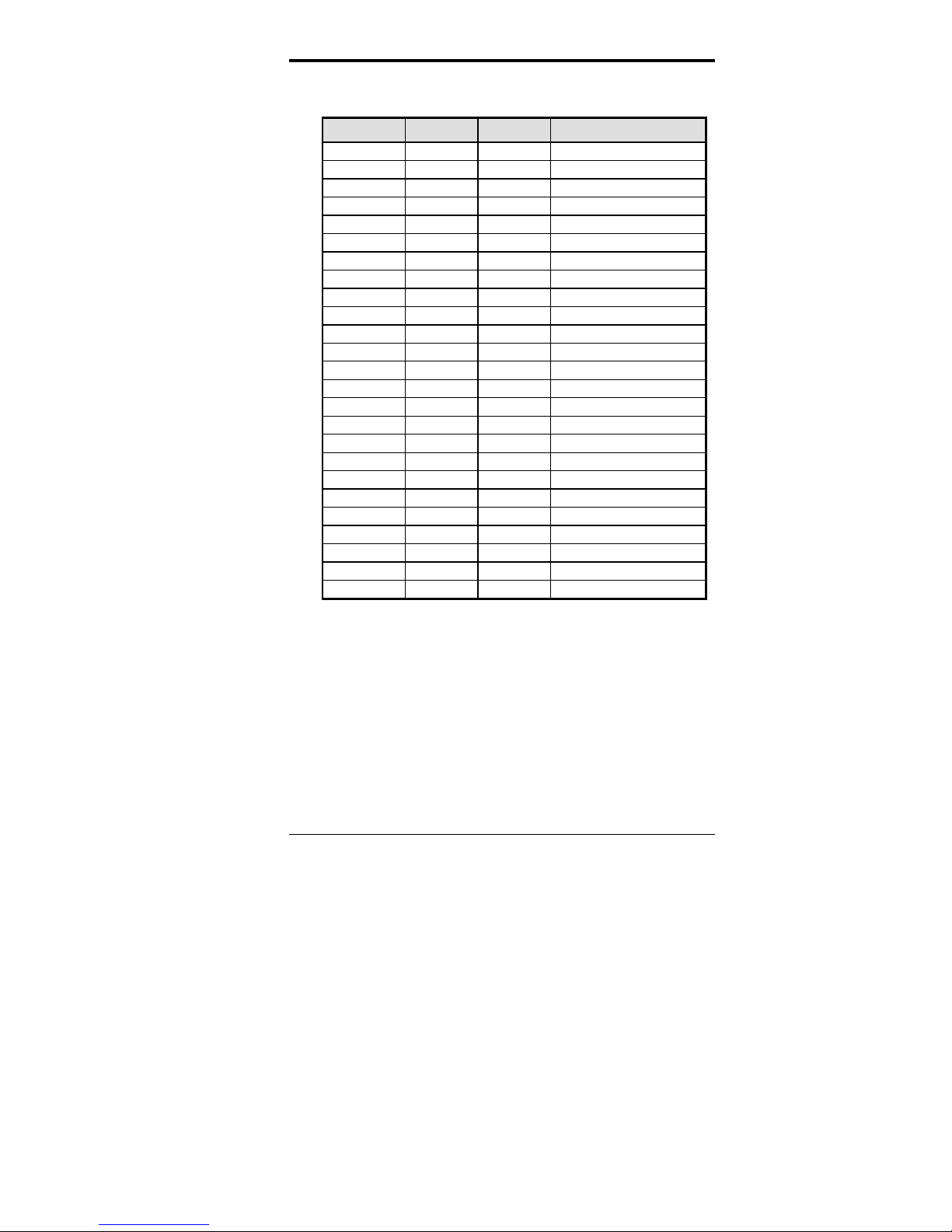
168Pin DIMM (3.3V) - SDRAM or EDO DRAM (continued)
DIMM3 DIMM2 DIMM1 Total Memory
64MB 16MB 16MB 96MB
128MB 16MB 16MB 160MB
32MB 32MB ----- 64MB
64MB 32MB ----- 96MB
128MB 32MB ----- 160MB
32MB 32MB 8MB 72MB
64MB 32MB 8MB 104MB
128MB 32MB 8MB 168MB
32MB 32MB 16MB 80MB
64MB 32MB 16MB 112MB
128MB 32MB 16MB 176MB
32MB 32MB 32MB 96MB
64MB 32MB 32MB 128MB
128MB 32MB 32MB 192MB
64MB 64MB ----- 128MB
128MB 64MB ----- 192MB
64MB 64MB 8MB 136MB
128MB 64MB 8MB 200MB
64MB 64MB 16MB 144MB
128MB 64MB 16MB 208MB
64MB 64MB 32MB 160MB
128MB 64MB 32MB 224MB
64MB 64MB 64MB 192MB
128MB 64MB 64MB 256MB
128MB 128MB 128MB 384MB
3.4 BIOS
The BIOS on the AI5VG+ motherboard provides the standard BIOS
functions plus the following additional features:
1. DMI (Desktop Management Interface)
The motherboard supports DMI to enable computer system management
in an enterprise.

Chapter 3 Hardware Description
10 AI5VG+ User’s Manual
2. ISA Plug and Play (PnP) Extension
Unlike PCI cards which are plug and play, ISA cards require setting
jumpers to resolve hardware conflicts. To make a computer system PnP,
an ISA PnP standard is established and supported by new OSes, such as
Windows 95. Under Windows 95, the motherboard BIOS must have ISA
PnP extension to support the new ISA PnP cards.
3. Power Management
The power management feature provides power savings by slowing down
the CPU clock, turning off the monitor screen and stopping the HDD
spindle motor.
3.5 Onboard PCI EIDE
The PCI EIDE controller is part of the MVP3 chipset. It supports PIO
mode 3/4 and bus mastering . The peak transfer rate of PIO mode 3/4 can
be as high as 17MB/sec. Using HDDs that support bus mastering, the
peak transfer rate can reach 22MB/sec. There are two IDE connectors,
primary IDE and secondary IDE. With two devices per connector, up to
four IDE drives are supported. The MVP3 also supports Ultra DMA/33,
a new “synchronous DMA” protocol for faster data transfers.
3.6 Onboard Multi-I/O
The onboard multi-I/O chip, Winbond W83877, supports two 16550
UART-compatible serial ports, one high speed EPP/ECP parallel port
and one floppy controller. The floppy controller supports 2.88MB
format. The I/O port addresses of the serial and parallel ports are
programmable via BIOS set-up.
3.7 Onboard CPU Temperature Sensor
The AD22105 IC on the motherboard is a temperature sensor for the
CPU. When the CPU temperature exceeds threshold value, the CPU
slows down automatically to allow it to cool down to a safe level.
Chapter 3 Hardware Description
AI5VG+ User’s Manual 11
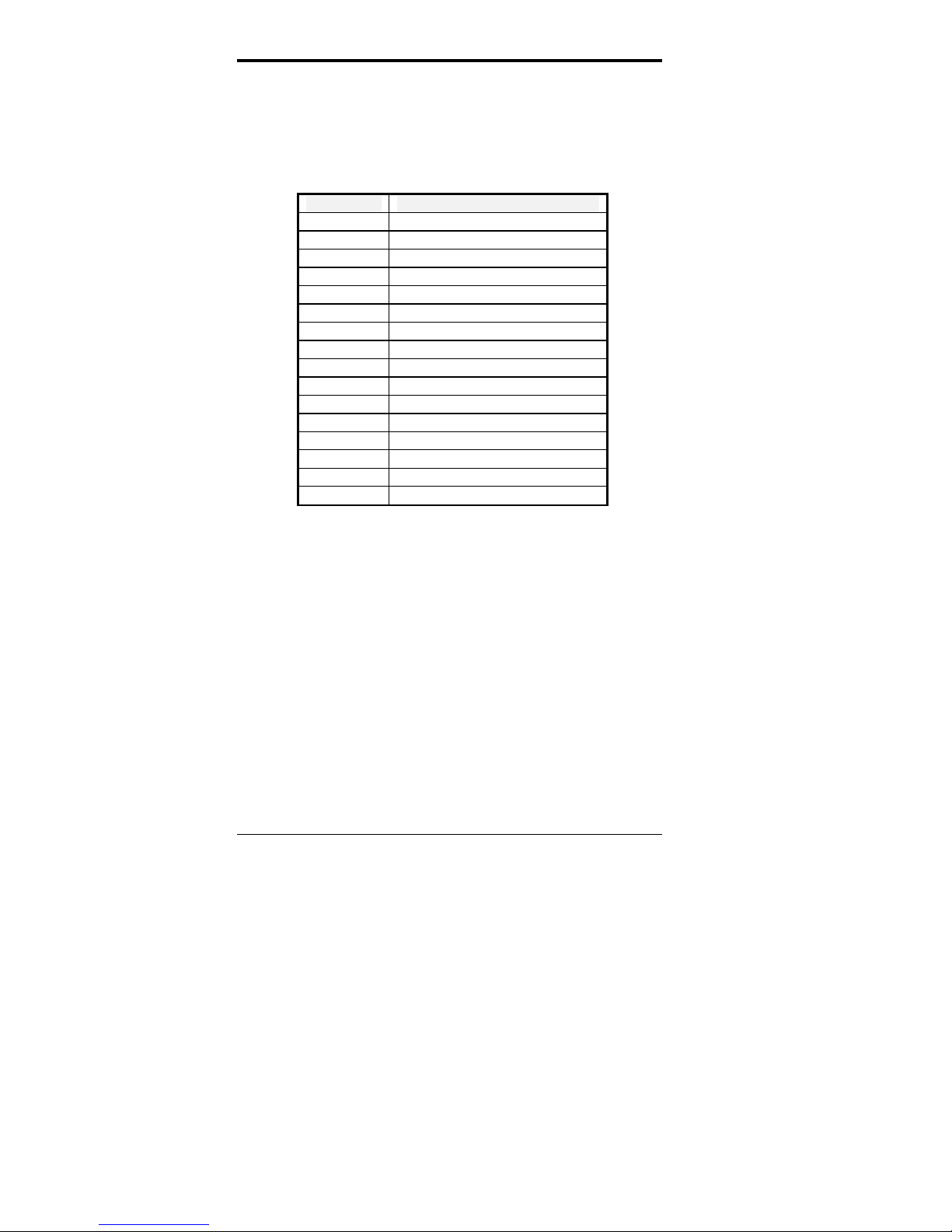
3.8 I/O Port Address Map
Each peripheral device in the system is assigned a set of I/O port
addresses which also becomes the identity of the device. There are a total
of 1K port address space available. The following table lists the I/O port
addresses used on the motherboard.
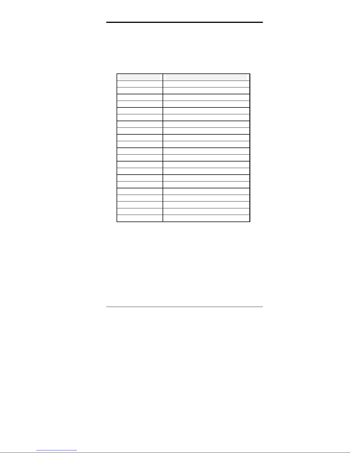
Address Device Description
000h - 01Fh DMA Controller #1
020h - 03Fh Interrupt Controller #1
040h - 05Fh Timer
060h - 06Fh Keyboard Controller
070h - 07Fh Real Time Clock, NMI
080h - 09Fh DMA Page Register
0A0h - 0BFh Interrupt Controller #2
0C0h - 0DFh DMA Controller #2
0F0h Clear Math Coprocessor Busy Signal
0F1h Reset Math Coprocessor
1F0h - 1F7h IDE Interface
278 - 27F Parallel Port #2 (LPT2)
2F8h - 2FFh Serial Port #2 (COM2)
2B0 - 2DF Graphics adapter Controller
378h - 3FFh Parallel Port #1(LPT1)
360 - 36F Network Ports
3B0 - 3BF Monochrome & Printer adapter
3C0 - 3CF EGA adapter
3D0 - 3DF CGA adapter
3F0h - 3F7h Floppy Disk Controller
3F8h - 3FFh Serial Port #1 (COM1)
3.9 DMA Channels
There are seven DMA Channels available on the motherboard. Only
DMA2 is used by the floppycontroller. In the case that ECP mode on the
parallel port is used, DMA1 or DMA3 will be used.
Chapter 3 Hardware Description
12 AI5VG+ User’s Manual
3.10 Interrupt Request Lines (IRQ)
There are a total of 15 IRQ lines available on the motherboard. Peripheral
devices use interrupt request lines to notify the CPU for the service
required. The following table shows the IRQ used by the devices on the
motherboard.
Level Function
IRQ0 System Timer Output
IRQ1 Keyboard
IRQ2 Interrupt Cascade
IRQ3 Serial Port #2
IRQ4 Serial Port #1
IRQ5 Parallel Port #2
IRQ6 Floppy Disk Controller
IRQ7 Parallel Port #1
IRQ8 Real Time Clock
IRQ9 Software Redirected to Int 0Ah
IRQ10 Reserved
IRQ11 Reserved
IRQ12 Reserved
IRQ13 80287
IRQ14 Primary IDE
IRQ15 Secondary IDE
3.11 Accelerated Graphics Port (AGP) Slot
The AI5VG+ motherboard comes with an AGP slot for an AGP VGA
card that supports 133MHz 2X mode for AD and SBA signaling to
provide high-performance 3D graphic display.

Chapter 5 Installation
AI5VG+ User’s Manual 13
Chapter 4 Hardware Settings
The following sections describe the necessary procedures and proper
jumper settings to configure the AI5VG+ motherboard.
4.1 SW1(1-8): CPU Frequency Selector.........................................15
4.2 JP1, SW1(4): DRAM Operating Frequency (AI5VG+-100).....20
4.3 JP6: System Frequency Divider (AI5VG+-100) .......................20
4.4 SW2(1-4): CPU Voltage Selector.............................................20
4.5 JP2: Clear CMOS Selection......................................................22
The AI5VG+-100MHz supports VIA’s MVP3 chipset and has a
maximumCPU bus speed of 100MHz. Please note the correct settings of
both the CPU and SDRAM clocks.
For the locations of the jumpers, refer to Figure 2 on the following page.
The following examples show the conventions used in this chapter
Jumper Open
Jumper Closed
Switch 1 and switch 2 are set to OFF.
Switch 3 and switch 4 are set to ON.
Chapter 5 Installation
14 AI5VG+ User’s Manual
Figure 2: Jumper Locations of the AI5VG+

Chapter 5 Installation
AI5VG+ User’s Manual 15
4.1 SW1(1-8): CPU Frequency Selector
For Intel Pentium, IDT WinChip 2-3D / C6
SW1 CPU
Clock AGP
Clock Multiplier CPU FREQ.
off on on xx off off off on
66MHz 66MHz 1.5x P54C-100
off on on xx on off off on
66MHz 66MHz 2x P54C-133
off on on xx on on off on
66MHz 66MHz 2.5x P54C/P55C-16
6
off on on off off on off on
66MHz 66MHz 3x
P54C/P55C-200
WinChip 2-3D
/ C6-200
off on on off off off off on
66MHz 66MHz 3.5x P55C-233
off off on off off on off on
75MHz 75MHz 3x
WinChip 2-3D
/ C6-225
off on on off on off on on
66MHz 66MHz 4x
WinChip 2-3D
266
off off off xx off on on off
100MHz 66MHz 2.33x
WinChip 2
266
off off off xx on on off off
100MHz 66MHz 2.5x
WinChip 2
300

Chapter 5 Installation
16 AI5VG+ User’s Manual
For Cyrix 6x86, 6x86L, 6x86MX CPU
SW1 CPU
Clock AGP
Clock Multiplier CPU FREQ.
off on on xx on off off on
66MHz 66MHz 2x P166+
(133MHz)
off off on xx on off off on
75MHz 64MHz 2x P200+
(150MHz)
off on on xx on on off on
66MHz 66MHz 2.5x
PR200
(166MHz)
off on on xx offon offon
66MHz 66MHz 3x
PR233
(200MHz)
off on on xx off off off on
66MHz 66MHz 3.5x
PR266
(233MHz)
off off on xx on on off on
75MHz 64MHz 2.5x
PR233
(187.5MHz)
off on off xx on on off off
83MHz 66MHz 2.5x
PR266
(208MHz)
off on off xx off on off off
83MHz 66MHz 3x
PR300
(250MHz)
Table of contents
Other TMC Motherboard manuals


