TMC MI7WBM SERIES User manual

MI7WBM SERIES
Socket 370 Intel 810/810E
Micro ATX Motherboard
User's Manual
Version 1.0A

ii MI7WBM User’s Manual
Copyright Notice
This publication is protected by copyright and all rights are reserved. No
part of it may be reproduced or transmitted by any means or in any form,
without prior consent of the original manufacturer.
The information in this document has been carefully checked and is
believed to be accurate. However, the original manufacturer assumes no
responsibility for any inaccuracies that may appear in this manual. In no
event will the original manufacturer be liable for direct, indirect, special,
exemplary, incidental, incidental or consequential damages resulting
from any defect or omission in this manual, even if advised of possibility
of such damages. The material contained herein is for informational
purposes only.
Acknowledgments
Award is a registered trademark of Award Software International, Inc.
PS/2 is a trademark of International Business Machines Corporation.
Intel and Celeron are registered trademarks of Intel Corporation.
Microsoft Windows is a registered trademark of Microsoft Corporation.
All other product names or trademarks are properties of their respective
owners.

Contents
MI7WBM User’s Manual iii
Contents
Chapter 1 Introduction....................................................1
Chapter 2 Specifications..................................................3
Chapter 3 Hardware Description ...................................5
3.1 Processor ...................................................................................7
3.2 L2 Cache ...................................................................................7
3.3 Main Memory............................................................................7
3.4 BIOS..........................................................................................8
3.5 Onboard VGA...........................................................................8
3.6 Hardware Monitoring................................................................8
3.7 Onboard Multi-I/O ....................................................................8
3.8 Interrupt Request (IRQ) Lines...................................................9
3.9 Onboard PCI-IDE......................................................................9
3.10 DMA Channels........................................................................9
3.11 I/O Port Address Map............................................................10
3.12 Onboard Audio......................................................................10
Chapter 4 Configuring the Motherboard ....................11
4.1 CPU Frequency Setting ...........................................................13
4.2 JP9: 100MHz CPU Host Frequency Force Selector................13
4.3 JP10: Clear CMOS Select .......................................................14
4.4 JP7: Boot Block Lock/Unlock.................................................14
4.5 JP8: Manufacturing Test Jumper.............................................14
4.6 JP16: Onboard Audio Enable/Disable.....................................14
4.7 JP17: Memory Clock Select....................................................15
4.8 JP19: CPU Select ....................................................................15
4.9 JP22, JP23: Celeron / Coppermine Select...............................16
4.10 5VSB and VCC LEDs...........................................................16
Chapter 5 Installation....................................................17
5.1 I/O Connectors ........................................................................19
5.2 CN1: PS/2 Keyboard and PS/2 Mouse Connectors.................19
5.3 CN2: USB Connector..............................................................20
5.4 CN3, CN7: Serial Ports...........................................................20
5.5 CN4: VGA Port Connector .....................................................21
5.6 CN5: Line Out, Line In, Mic In, Game Port............................21
5.7 CN6: Parallel Port Connector..................................................22

Contents
iv MI7WBM User’s Manual
5.8 CN8: Front Bezel Connectors..................................................22
5.9 FDC: Floppy Drive Connector.................................................24
5.10 IDE1, IDE2: EIDE Connectors..............................................25
5.11 J6: ATX Power Supply Connector ........................................26
5.12 F5: Chip Fan Power Connector..............................................26
5.13 F6: CPU Fan Power Connector..............................................26
5.14 F7: Chassis Fan Power Connector.........................................26
5.15 JP2: IrDA Connector.............................................................27
5.16 JP3, JP4: CD-ROM Audio In Connectors .............................27
5.17 JP5: Wake on LAN Connector ..............................................27
Chapter 6 BIOS Configuration.....................................29
6.1 BIOS Introduction ...................................................................32
6.2 BIOS Setup..............................................................................32
6.3 Standard CMOS Setup.............................................................34
6.4 Advanced BIOS Features.........................................................37
6.5 Advanced Chipset Features......................................................40
6.6 Integrated Peripherals..............................................................42
6.7 Power Management Setup .......................................................45
6.8 PNP/PCI Configurations..........................................................48
6.9 PC Health Status......................................................................49
6.10 Frequency/Voltage Control....................................................50
6.11 Load Fail-Safe Defaults.........................................................51
6.12 Load Setup Defaults...............................................................51
6.13 Set Supervisor/User Password...............................................52
6.14 Save & Exit Setup..................................................................53
6.15 Exit Without Saving...............................................................53
Chapter 7 Intel 810 Drivers Installation......................55
Installing Intel 82810 Define Drivers for Windows 95/98..............56
Installing Intel 82810 VGA Driver for Windows 95/98.................59
Installing Intel 82810 VGA Driver for Windows NT.....................62
Installing Intel 82810 Audio Driver for Windows 95/98................64
Installing Intel 82810 Audio Driver for Windows NT 4.0..............74
Appendix..........................................................................75
Chapter 1 Introduction
MI7WBM User’s Manual 1
Chapter 1 Introduction
This manual is designed to give you information on the MI7WBM
motherboard. It is divided into the following sections:
•
••
•
Introduction
•
••
•
Specifications
•
••
•
Hardware Description
•
••
•
Configuring the Motherboard
•
••
•
Installation
•
••
•
BIOS Configuration
•
••
•
Intel 810 Drivers Installation
Checklist
Please check that your package is complete and contains the items below.
If you discover damaged or missing items, please contact your dealer.
The MI7WBM Motherboard
1 IDE ribbon cable with UDMA66 support
1 floppy ribbon cable
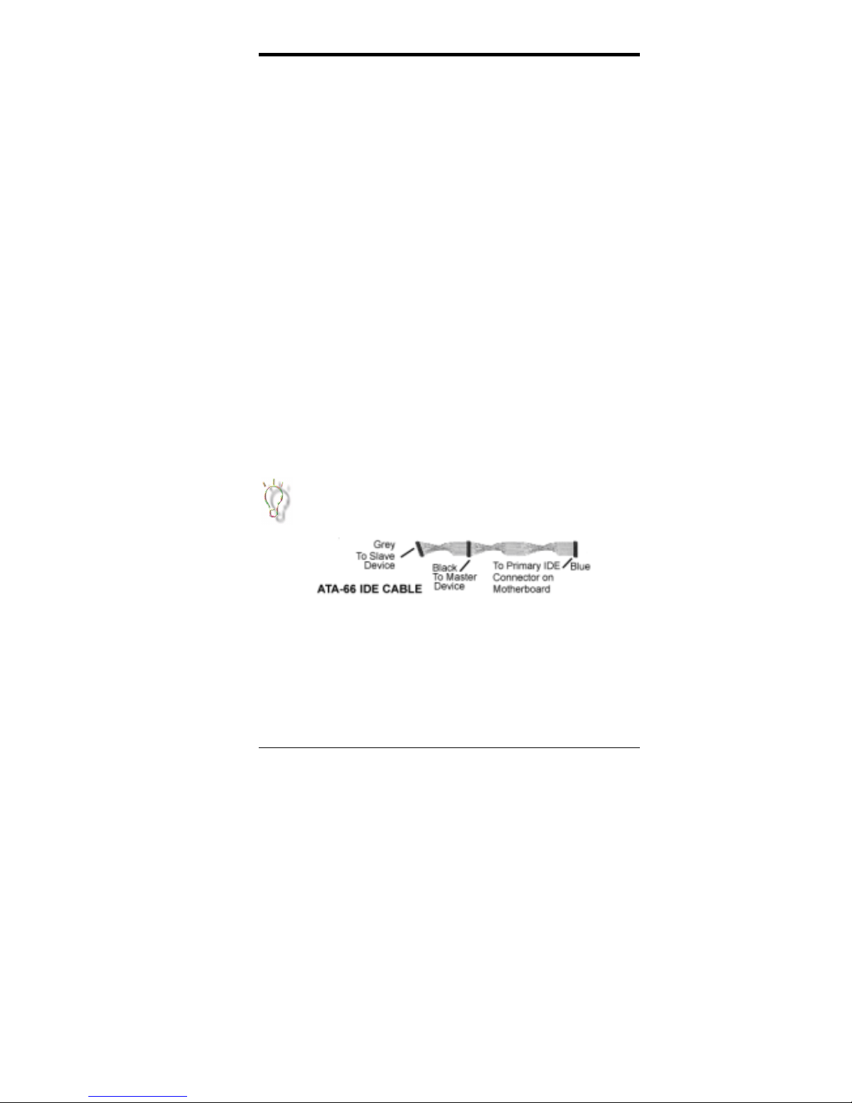
The ATA-66 IDE cable is used in conjunction with Ultra DMA/66
hard disks. Refer to the figure below on howto connect the cable.

Chapter 1 Introduction
2MI7WBM User’s Manual
Product Information
MODEL NO. Features
Intel 810 DC100 with 4MB display memory
Supports Suspend to RAM (STR)
MI7WBM series Supports 66/100MHz Front Side Bus
Supports Ultra DMA33/66
Intel 810
Does not support Suspend to RAM (STR)
MI7WBML series Supports 66/100MHz Front Side Bus
Supports Ultra DMA33/66
Intel 810E
Supports Suspend to RAM (STR)
MI7WBME series Supports 66100/133MHz Front Side Bus
Supports Ultra DMA33/66

Chapter 2 Specifications
MI7WBM User’s Manual 3
Chapter 2 Specifications
The MI7WBM is a high-performance Micro ATX Intel 810 motherboard
with a Socket 370 connector for Intel Celeron/Coppermine processors.
The motherboard offers flexibility in terms of CPU frequency and main
memory type and size. The main features of the motherboard consist of
the following:
CPU Socket
Socket 370
Chipset
Intel 810 / 810E
Processor
Intel Celeron / Coppermine
300 ~ 600MHz or higher when available
Bus Speed
66/100MHz (for 810 chipset)
66/100/133MHz (for 810E chipset)
L2 Cache
CPU integrated L2 cache
Main Memory
Two 168-pin DIMM sockets
Memory types: SDRAM (Synchronous DRAM)
Memory sizes: 64MB, 128MB
Chipset
Intel 810 chipset with built-in PCI-IDE
Super I/O
Built-in Winbond 83627HF chip
z
Two 16550 UART compatible serial ports
z
One parallel port (ECP/EPP compatible)
z
One floppy controller (2.88MB compatible)
z
One IrDA port

Chapter 2 Specifications
4MI7WBM User’s Manual
PCI Bus Master IDE Controller
The onboard chipset’s PCI Bus Master IDE controller with two
connectors for up to four IDE devices in two channels, supporting
enhanced IDE devices such as tape backup and CD-ROM drives, PIO
Mode 3/4 and Bus Mastering Ultra DMA/66 / Ultra DMA/33.
Note: A UDMA66 cable should be used for UDMA66 interface. Under
Windows NT 4.0, you need to install Windows NT Service Pack 5.)
BIOS
Award BIOS with ISA Plug and Play (PnP) extension, DMI, bootable
CD-ROM and power-management features. The BIOS is Y2K (Year
2000) compliant.
Mouse Connector
PS/2 type
Keyboard Connector
PS/2 type
USB Connector
2 ports on board
Win95/98 shut-off
Allows shut-off control from within Windows 95/98
Onboard Audio
Onboard AC97 Codec
Onboard VGA
The highly integrated graphics accelerator consists of dedicated
multimedia engines executing in parallel to deliver high performance
3D, 2D and motion compensation video capabilities. The 3D and 2D
engines are managed by a 3D/2D pipeline preprocessor allowing a
sustained flow of graphics data to be rendered and displayed. It also
features a 4MB display cache buffer.
Expansion Slots
Three 32-bit PCI slots
One AMR slot for modem
Form Factor
Micro ATX, 9.65” x 7.87” (24.5cm x 20cm)

Chapter 3 Hardware Description
MI7WBM User’s Manual 5
Chapter 3 Hardware Description
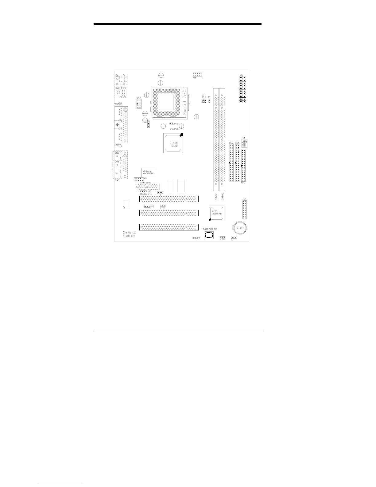
This chapter brieflydescribes each of the major featuresof the MI7WBM
motherboard. The layout of the board in Figure 1 shows the location of
the key components. The topics covered in this chapter are as follows:
3.1 Processor ...................................................................................7
3.2 L2 Cache ...................................................................................7
3.3 Main Memory............................................................................7
3.4 BIOS..........................................................................................8
3.5 Onboard VGA...........................................................................8
3.6 Hardware Monitoring................................................................8
3.7 Onboard Multi-I/O ....................................................................8
3.8 Interrupt Request (IRQ) Lines...................................................9
3.9 Onboard PCI-IDE......................................................................9
3.10 DMA Channels........................................................................9
3.11 I/O Port Address Map............................................................10
3.12 Onboard Audio......................................................................10
Chapter 3 Hardware Description
6MI7WBM User’s Manual
Figure 1: Layout of the MI7WBM Motherboard

Chapter 3 Hardware Description
MI7WBM User’s Manual 7
3.1 Processor
The MI7WBM motherboard is designed to take an Intel Celeron
processor running 300/333/350/366/400/433/450/466/500MHz.
3.2 L2 Cache
The L2 cache is integrated in the processor.
3.3 Main Memory
The MI7WBM motherboard supports two 168-pin DIMM (Dual In-line
MemoryModule) sockets to forma memory configuration from 64MB to
256MB. DIMM modules can be 64M and128MB in SDRAM. In
populating the DIMM sockets, any socket can be populated first. Refer to
the following table on how to do the memory configuration.
(DIMM1) (DIMM2) Total Memory
64MB ----- 64MB
128MB ----- 128MB
64MB 64MB 128MB
128MB 64MB 192MB
128MB 128MB 256MB
Use SDRAM modules with PC100 specification only when
running either 66MHz or100MHz CPU bus speed.
The red LED indicator beside the DIMM memory sockets
determine if there is electric current in the memory. Before
removing or installing a memory module, make sure that this LED
indicator is notON. If theLED light is on, please turn off the power
or unplugged the power cable.

Chapter 3 Hardware Description
8MI7WBM User’s Manual
3.4 BIOS
The BIOS on the MI7WBM motherboard provides the standard BIOS
functions plus the following feature:
Power Management
The power management feature provides power savings by slowing
down the CPU clock, turning off the monitor screen and stopping the
HDD spindle motor. The BIOS fully conforms to ACPI (Advanced
Configuration and Power Interface) specification.
3.5 Onboard VGA
The highly integrated graphics accelerator consists of dedicated
multimedia engines executing inparallel to deliver high performance 3D,
2D and motion compensation video capabilities. The 3D and 2D engines
are managedby a 3D/2D pipeline preprocessor allowing a sustained flow
sustained flow of graphics data to be rendered and displayed. It also
features a 4MB display cache buffer.
3.6 Hardware Monitoring
The Winbond 83627HFchip has a built-in hardware status monitoring
function that monitor several hardware parameters including power
supply voltages, fan speeds, and temperatures, which are very important
for a high-end computer system to work stable and properly. This
function is used together with System Monitor utilityor the optional Intel
LANDesk Client Manager utility.
3.7 Onboard Multi-I/O
The multi-I/O function is built in the Winbond 83627HF chip supports a
keyboard controller, two serial ports, one parallel port, one floppy
controller and one IrDA port. The serial ports are 16550 UART
compatible. The parallel port features high-speed EPP/ECP mode. The
floppy controller supports up to 2.88MB format.

Chapter 3 Hardware Description
MI7WBM User’s Manual 9
3.8 Interrupt Request (IRQ) Lines
There are a total of 15 IRQ lines available on the motherboard. Peripheral
devices use an interrupt request to notify the CPU for the service
required. The following table shows the IRQ lines used bythe devices on
the motherboard:
Level Function
IRQ0 System Timer Output
IRQ1 Keyboard
IRQ2 Interrupt Cascade
IRQ8 Real Time Clock
IRQ9 Software Redirected to Int 0Ah
IRQ10 Reserved
IRQ11 Reserved
IRQ12 Reserved
IRQ13 Co-Processor
IRQ14 Primary IDE
IRQ15 Secondary IDE
IRQ3 INTERRUPT
IRQ4 Serial Port #1
IRQ5 INTERRUPT
IRQ6 Floppy Disk Controller
IRQ7 Parallel Port #1
3.9 Onboard PCI-IDE
The Intel 810 chipset’s built-in’s PCI-IDE controller supports PIO mode
3/4 and bus mastering Ultra DMA/66 / Ultra DMA/33. The peak transfer
rate of PIO mode 3/4 can be as high as 17MB/sec. Using HDDs that
support Ultra DMA/66, the peak transfer rate can reach 66MB/sec. The
peak transfer rate of PIO mode 3/4 can be as high as 17MB/sec. There are
twoIDE connectors - primary IDE and secondaryIDE. With two devices
per connector, up to four IDE devices can be supported.
3.10 DMA Channels
There are seven DMA channels available on the motherboard; only
DMA2 is used by the floppycontroller. In the case that ECP mode on the
parallel port is utilized, DMA1 or DMA3 will be used.

Chapter 3 Hardware Description
10 MI7WBM User’s Manual
3.11 I/O Port Address Map
Each peripheral device in the system is assigned a set of I/O port
addresses, which also becomes the identity of the device. There is a total
of 1K port address space available. The following table lists the I/O port
addresses used on the motherboard.
Address Device Description
000h - 01Fh DMA Controller #1
020h - 03Fh Interrupt Controller #1
040h - 05Fh Timer
060h - 06Fh Keyboard Controller
070h - 07Fh Real Time Clock,, NMI
080h - 09Fh DMA Page Register
0A0h - 0BFh Interrupt Controller #2
0C0h - 0DFh DMA Controller #2
0F0h Clear Math Coprocessor Busy Signal
0F1h Reset Math Coprocessor
1F0h - 1F7h IDE Interface
2F8h - 2FFh Serial Port #2(COM2)
378h - 3FFh Parallel Port #1(LPT1)
3F0h - 3F7h Floppy Disk Controller
3F8h - 3FFh Serial Port #1(COM1)
3.12 Onboard Audio
Onboard AC97 Codec

Chapter 4 Configuring the Motherboard
MI7WBM User’s Manual 11
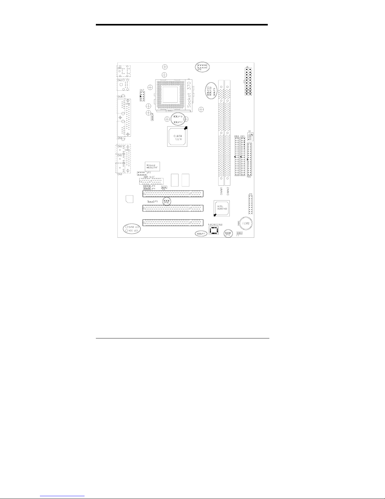
Chapter 4 Configuring the Motherboard
The following sections describe the necessary procedures and proper
jumper settings to configure the MI7WBM motherboard. For the
locations of the jumpers, refer to Figure 2.
4.1 CPU Frequency Setting ...........................................................13
4.2 JP9: 100MHz CPU Host Frequency Force Selector................13
4.3 JP10: Clear CMOS Select .......................................................14
4.4 JP7: Boot Block Lock/Unlock.................................................14
4.5 JP8: Manufacturing Test Jumper.............................................14
4.6 JP16: Onboard Audio Enable/Disable.....................................14
4.7 JP17: Memory Clock Select....................................................15
4.8 JP19: CPU Select ....................................................................15
4.9 JP22, JP23: Celeron / Coppermine Select...............................16
4.10 5VSB and VCC LEDs...........................................................16
The following examples show the conventions used in this chapter.
Jumper Open
Jumper Closed/Short
Chapter 4 Configuring the Motherboard
12 MI7WBM User’s Manual
Figure 2: Jumper Location on the MI7WBM
Chapter 4 Configuring the Motherboard
MI7WBM User’s Manual 13
4.1 CPU Frequency Setting
The MI7WBM uses jumper-free technology in configuring the processor
on the motherboard. The system automatically detects the CPU bus
speed, 66MHz or 100MHz and sets the multiplier, or ratio, to 3X.
However, the bus speed can also be configured through the BIOS if the
processor supports this feature. The BIOS (under CPU Features Setup)
allows users to change the CPU bus speed multiplier (3X, 3.5X, 4X,
4.5X, 5X, 5.5X, 6X, 6.5X, 7X, 7.5X, 8X) to set the correct or desired
CPU frequency. The CPU bus speed multiplier will remain unchanged if
the CPU installed supports a fixed (only one) bus speed multiplier.
It is possible that the system will not boot if the CPU has been
changed. When this happens, turn off the computer by pressing
the power button and turn it on again by pressing the Insert key
and the power button simultaneously. (Note to press the Insert
key until an image appears on the screen.) When the system is
turned on, press the Delete key to enter BIOS Setup and
configure the CPU speed.
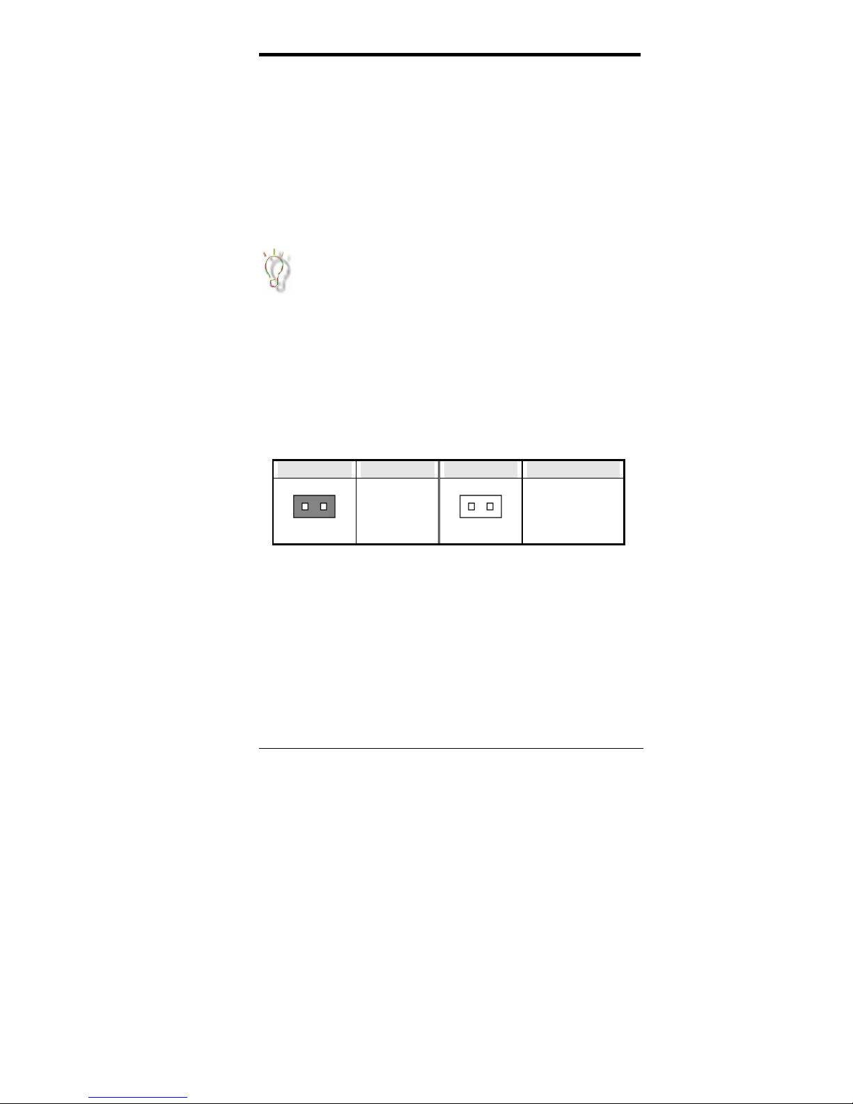
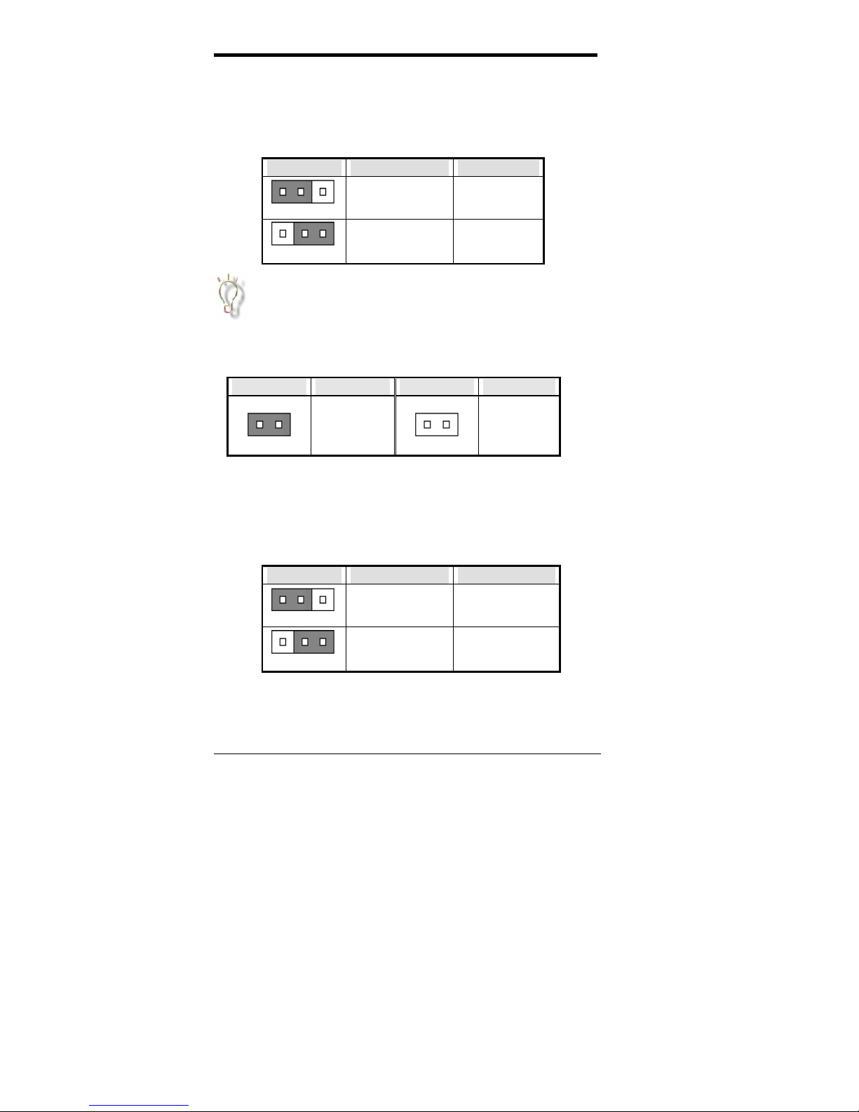
4.2 JP9: 100MHz CPU Host Frequency Force Selector
The MI7WBM is able to detect the host frequency (66MHz or 100MHz)
of the installed CPU. The JP9 jumper, however, can be set to OPEN to
override the detection and force the host frequency to run at 100MHz.
JP9 Function JP9 Function
SHORT
Host
Frequency
Auto-detect
(default)
OPEN
Host Frequency
set to 100MHz
Chapter 4 Configuring the Motherboard
14 MI7WBM User’s Manual
4.3 JP10: Clear CMOS Select
Use JP10, a 3-pin header, to clear the contents of the CMOS RAM. Do
not clear the CMOS RAM unless it is absolutely necessary. You will lose
your password, etc.
JP10 Jumper Setting Function
1 2 3
pin 1-2: short Clear CMOS
1 2 3 pin 2-3: short Normal
To clear CMOS, the power connector should be disconnected
from the motherboard.
4.4 JP7: Boot Block Lock/Unlock
When the Boot Block is locked, BIOS flash update cannot be executed.
JP7 Function JP7 Function
SHORT
Boot Block
Unlock
OPEN
Boot Block
Lock
4.5 JP8: Manufacturing Test Jumper
The 10-pin JP8 jumper is for manufacturing testing use only and should
be left as is.
4.6 JP16: Onboard Audio Enable/Disable
JP16 Jumper Setting Function
1 2 3
pin 1-2: short Onboard Audio
Disabled
1 2 3 pin 2-3: short Onboard Audio
Enabled

Chapter 4 Configuring the Motherboard
MI7WBM User’s Manual 15
4.7 JP17: Memory Clock Select
For MI7WBM Series Ver. 1.00
The MI7WBM comes with the JP17 memory clock select jumper. In case
you are using 64MB NEC or LGS SDRAM module and the system does
not boot, set JP17 to SHORT to delay the memory clock.
For MI7WBM Series Ver. 1.20
1.When only one DIMM slot is used, leave JP17 OPEN
2.When 2 DIMM slots are used, set JP17 to SHORT.
3.When using NEC DIMM modules, regardless one or two DIMM slots
are used, JP17 should be set to SHORT.
4.When using CPU bus speed of 66MHz, leave JP17 OPEN.
IMPORTANT NOTES:
1. If the memory module you are using is not included in our test report
or is an ‘unknown’ brand, set JP17 to OPEN first. (It is recommended to
use PC-100 compatible memory modules.) If the system does not boot,
then set JP17 to short.
2. Regardlessof the brand of memory module you are using, they must be
PC-100 compatible modules.
3. In the BIOS setup on page 40, there is an option for the SDRAM cycle
time. Its setting must meet the specification of your SDRAM module. Or
else, the system might become unstable.
4. If your CPU uses 100MHz bus speed, JP17 should be SHORT.
4.8 JP19: CPU Select
The JP19 2-pin jumper is used in conjunction with the processor installed
on the motherboard. When the processor is an Intel Coppermine/Celeron
processor with 128K cache, JP19 should be OPEN. For an Intel
Coppermine processor with 256K cache, JP19 should be
CLOSED/SHORT.
JP19 Function JP19 Function
OPEN
Coppermine/
Celeron with
128K cache
SHORT
Coppermine
with 256K
cache

Chapter 4 Configuring the Motherboard
16 MI7WBM User’s Manual
4.9 JP22, JP23: Celeron / Coppermine Select
The default setting of the JP22 and JP23 2-pin jumpers are SHORT,
which setting is used for Intel Coppermine and Intel Celeron CPUs.
However, for Intel Celeron processors with CPU ID 066X, JP22 and
JP23 should be left OPEN.
The JP22 and JP23 jumpers can be found only in MI7WBM Series
Ver. 1.20.
4.10 5VSB and VCC LEDs
The 5VSB LED light is on to indicate that there is suspend power signal
fromthe power supply. The VCCLED light is onto indicate the power is
on.
Table of contents
Other TMC Motherboard manuals


