TMC MI7VGA User manual

MI7VGA
Socket 370 Apollo Pro
Micro ATX Motherboard
User's Manual
Version 1.0

Copyright Notice
This publication is protected by copyright and all rights are reserved.
No part of it may be reproduced or transmitted by any means or in any
form, without prior consent of the original manufacturer.
The information in this document has been carefully checked and is
believed to be accurate. However, the original manufacturer assumes
no responsibility for any inaccuracies that may appear in this manual.
n no event will the original manufacturer be liable for direct, indirect,
special, exemplary, incidental, incidental or consequential damages
resulting from any defect or omission in this manual, even if advised of
possibility of such damages. The material contained herein is for
informational purposes only.
Acknowledgments
Award is a registered trademark of Award Software nternational, nc.
PS/2 is a trademarks of nternational Business Machines Corporation.
ntel and Celeron are registered trademarks of ntel Corporation.
Apollo Pro is a trademark of V A Technologies.
Microsoft Windows is a registered trademark of Microsoft Corporation.
All other product names or trademarks are properties of their respective
owners.
ii MI7VGA User’s Manual

Contents
Contents
hapter 1 Introduction.....................................................1
hapter 2 Specifications...................................................3
hapter 3 Hardware Description....................................5
3.1 Processor....................................................................................7
3.2 L2 Cache....................................................................................7
3.3 Main Memory.............................................................................7
3.4 B OS...........................................................................................9
3.5 Onboard AGP Slot.....................................................................9
3.6 Hardware Monitoring.................................................................9
3.7 Onboard Multi- /O.....................................................................9
3.8 nterrupt Request ( RQ) Lines..................................................10
3.9 Onboard PC - DE.....................................................................10
3.10 DMA Channels.......................................................................10
3.11 /O Port Address Map............................................................11
3.12 Onboard Audio.......................................................................11
hapter 4 onfiguring the Motherboard.....................13
4.1 CPU Frequency Setting............................................................15
4.2 Clear CMOS Select: JP5..........................................................15
4.3 JP3: SDRAM Clock Select.......................................................16
4.4 CPU Host Frequency Force Selector: JP4................................16
hapter 5 Installation.....................................................17
5.1 /O Connectors.........................................................................19
5.2 J1: PS/2 Keyboard and PS/2 Mouse Connectors.....................19
5.3 J2: USB Connector...................................................................20
5.4 J3, J5: Serial Ports....................................................................20
5.5 J4: Parallel Port Connector.......................................................21
5.6 J6, J7, J8, J9: Line Out, Line n, Mic n, Game Port...............21
5.7 DE1, DE2: E DE Connectors................................................22
5.8 J10: CPU Fan Power Connector...............................................23
5.9 J11: Floppy Drive Connector...................................................23
5.10 J12: Wake on LAN Connector...............................................24
5.11 J13: ATX Power Supply Connector.......................................24
5.12 J14: AGP Fan Power Connector.............................................24
5.13 J16: Auxiliary Audio n Connectors......................................25
MI7VGA User’s Manual iii

Contents
5.15 J19: rDA Connector..............................................................25
5.16 J21: Chassis Fan Power Connector........................................26
5.17 J22: Front Bezel Connectors..................................................26
hapter 6 BIOS onfiguration.....................................29
6.1 B OS ntroduction....................................................................32
6.2 B OS Setup...............................................................................32
6.3 Standard CMOS Setup.............................................................34
6.4 B OS Features Setup................................................................37
6.5 Chipset Features Setup.............................................................40
6.6 Power Management Setup........................................................42
6.7 PNP/PC Configuration............................................................45
6.8 Load B OS Defaults.................................................................47
6.9 Load Setup Defaults.................................................................47
6.10 CPU Features Setup................................................................48
6.11 ntegrated Peripherals.............................................................50
6.12 Supervisor / User Password....................................................52
6.13 DE HDD Auto Detection......................................................53
6.14 Save & Exit Setup..................................................................54
6.15 Exit Without Saving...............................................................54
hapter 7 VIA Drivers Installation Guide...................55
7.1 4-in-1 Drivers nstallation........................................................55
7.2 Audio Drivers nstallation........................................................62
Audio Driver nstallation for Windows 95.........................62
Audio Driver nstallation for Windows 98.........................66
Audio Driver nstallation for Windows NT 4.0..................69
7.3 DirectX Driver nstallation.......................................................72
Appendix...........................................................................75
A. Additions & Errata....................................................................75
iv MI7VGA User’s Manual

Chapter 1 Introduction
hapter 1 Introduction
This manual is designed to give you information on the M 7VGA
motherboard. t is divided into the following sections:
Introduction
Specifications
Hardware Description
onfiguring the Motherboard
Installation
BIOS onfiguration
VIA Drivers Installation Guide
hecklist
Please check that your package is complete and contains the items
below. f you discover damaged or missing items, please contact your
dealer.
The M 7VGA Motherboard
1 DE ribbon cable
1 floppy ribbon cable
1 CD containing PC RQ Routing Miniport driver, VXD
(GART) driver, Bus Master DE driver and utilities.
MI7VGA User’s Manual 1

This page was intentionally left blank.
2 MI7VGA User’s Manual

Chapter 2 Specifications
hapter 2 Specifications
The M 7VGA is a high-performance Micro ATX Apollo Pro
motherboard with a Socket 370 connector for ntel Celeron processors.
The VT82C686A chip that comes with the Apollo Pro chipset has
built-in multi /O, audio and hardware monitoring functions. The
motherboard offers flexibility in terms of CPU frequency and main
memory type and size. The main features of the motherboard consist of
the following:
PU Socket
Socket 370
Processor
ntel Celeron
300/333/350/366/400/433/450/466/500MHz CPU frequency
Bus Speed
66/100MHz
L2 ache
CPU integrated L2 cache
Main Memory
Three 168-pin D MM sockets
Memory types: Extended Data Output (EDO) DRAM, SDRAM
(Synchronous DRAM)
Memory size: 8MB, 16MB, 32MB, 64MB, 128MB
hipset
V A’s Apollo Pro chipset (VT82C691 + VT82C686A) with built-in
PC - DE
Super I/O
Built-in V A’s VT82C686A chip
Two 16550 UART compatible serial ports
One parallel port (ECP/EPP compatible)
One floppy controller (2.88MB compatible)
One rDA port
MI7VGA User’s Manual 3

Chapter 2 Specifications
P I Bus Master IDE ontroller
The onboard V A chipset’s PC Bus Master DE controller with two
connectors for up to four DE devices in two channels, supporting
enhanced DE devices such as tape backup and CD-ROM drives,
P O Mode 3/4 and Bus Mastering Ultra DMA/66 / Ultra DMA/33.
Note: A UDMA66 cable should be used for UDMA66 interface.
Under Windows NT 4.0, you need to install Windows NT ervice
Pack 4.)
BIOS
Award B OS with SA Plug and Play (PnP) extension, DM ,
bootable CD-ROM and power-management features. The B OS is
Y2K (Year 2000) compliant.
Mouse onnector
PS/2 type
Keyboard onnector
PS/2 type
USB onnector
2 ports on board
Win95-shut-off
Allows shut-off control from within Windows 95
Onboard Audio
Built-in V A’s VT82C686A
The onboard audio is fully compatible with Sound Blaster Pro
compliant with ntel PC97 specifications.
Onboard AGP Slot
The AGP (Accelerated Graphics Port) slot supports AGP compliant
VGA cards to achieve rich 3D and video graphics display. AGP is a
platform bus specification that enables 3D graphics capabilities
including support for z-buffering, alpha blending and faster texture
mapping.
Expansion Slots
Three 32-bit PC slots
One 16-bit SA slots
One AGP slot
Form Factor
Micro ATX, 9.65” x 7.48 (24.5cm x 19cm)
4 MI7VGA User’s Manual

Chapter 3 ardware Description
hapter 3 Hardware Description
This chapter briefly describes each of the major features of the
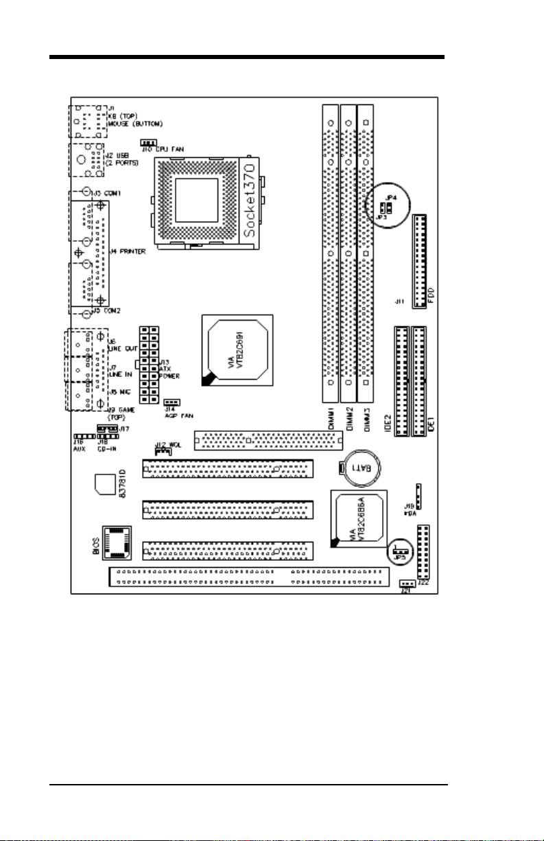
M 7VGA motherboard. The layout of the board in Figure 1 shows the
location of the key components. The topics covered in this chapter are
as follows:
3.1 Processor....................................................................................7
3.2 L2 Cache....................................................................................7
3.3 Main Memory.............................................................................7
3.4 B OS...........................................................................................9
3.5 Onboard AGP Slot.....................................................................9
3.6 Hardware Monitoring.................................................................9
3.7 Onboard Multi- /O.....................................................................9
3.8 nterrupt Request ( RQ) Lines..................................................10
3.9 Onboard PC - DE.....................................................................10
3.10 DMA Channels.......................................................................10
3.11 /O Port Address Map............................................................11
3.12 Onboard Audio.......................................................................11
MI7VGA User’s Manual 5

Chapter 3 ardware Description
Figure 1: Layout of the MI7VGA Motherboard
6 MI7VGA User’s Manual

Chapter 3 ardware Description
3.1 Processor
The M 7VGA motherboard is designed to take an ntel Celeron
processor running 300/333/350/366/400/433/450/466/500MHz.
3.2 L2 ache
The L2 cache is integrated in the processor.
3.3 Main Memory
The M 7VGA motherboard supports three 168-pin D MM (Dual n-
line Memory Module) sockets to form a memory configuration from
8MB to 384MB. D MM modules can be 8MB, 16MB, 32MB, 64M
and128MB in SDRAM. n populating the D MM sockets, any socket
can be populated first. Refer to the following table on how to do the
memory configuration.
NOTE: Use DRAM modules with PC100 specification when running
100MHz CPU bus speed. With 66MHz CPU bus speed,
DRAM modules with PC66 or PC100 specification can be
used.
(DIMM1) (DIMM2) (DIMM3) Total Memory
8MB ----- ----- 8MB
16MB ----- ----- 16MB
32MB ----- ----- 32MB
64MB ----- ----- 64MB
128MB ----- ----- 128MB
8MB 8MB ----- 16MB
16MB 8MB ----- 24MB
32MB 8MB ----- 40MB
64MB 8MB ----- 72MB
128MB 8MB ----- 136MB
8MB 8MB 8MB 24MB
16MB 8MB 8MB 32MB
32MB 8MB 8MB 48MB
64MB 8MB 8MB 80MB
128MB 8MB 8MB 144MB
16MB 16MB ----- 32MB
32MB 16MB ----- 48MB
MI7VGA User’s Manual 7
Chapter 3 ardware Description
64MB 16MB ----- 80MB
128MB 16MB ----- 144MB
16MB 16MB 8MB 40MB
32MB 16MB 8MB 56MB
64MB 16MB 8MB 88MB
128MB 16MB 8MB 152MB
16MB 16MB 16MB 48MB
32MB 16MB 16MB 64MB
64MB 16MB 16MB 96MB
128MB 16MB 16MB 160MB
32MB 32MB ----- 64MB
64MB 32MB ----- 96MB
128MB 32MB ----- 160MB
32MB 32MB 8MB 72MB
64MB 32MB 8MB 104MB
128MB 32MB 8MB 168MB
32MB 32MB 16MB 80MB
64MB 32MB 16MB 112MB
128MB 32MB 16MB 176MB
32MB 32MB 32MB 96MB
64MB 32MB 32MB 128MB
128MB 32MB 32MB 192MB
64MB 64MB ----- 128MB
128MB 64MB ----- 192MB
64MB 64MB 8MB 136MB
128MB 64MB 8MB 200MB
64MB 64MB 16MB 144MB
128MB 64MB 16MB 208MB
64MB 64MB 32MB 160MB
128MB 64MB 32MB 224MB
64MB 64MB 64MB 192MB
128MB 64MB 64MB 256MB
128MB 128MB 128MB 384MB
8 MI7VGA User’s Manual

Chapter 3 ardware Description
3.4 BIOS
The B OS on the M 7VGA motherboard provides the standard B OS
functions plus the following additional features:
1. ISA Plug and Play (PnP) Extension
Unlike PC cards that are Plug and Play, SA cards require setting
jumpers to resolve hardware conflicts. To make a computer system
PnP, an SA PnP standard is established and supported by new
operating systems, such as Windows 95. Under Windows 95, the
motherboard B OS must have an SA PnP extension to support new
SA PnP cards.
2. Power Management
The power management feature provides power savings by slowing
down the CPU clock, turning off the monitor screen and stopping
the HDD spindle motor. The B OS fully conforms to ACP
(Advanced Configuration and Power nterface) specification.
3.5 Onboard AGP Slot
The AGP (Accelerated Graphics Port) slot supports AGP compliant
VGA cards to achieve rich 3D and video graphics display. AGP is a
platform bus specification that enables 3D graphics capabilities
including support for z-buffering, alpha blending and faster texture
mapping.
3.6 Hardware Monitoring
The V A VT82C686A chip has a built-in hardware status monitoring
function that monitor several hardware parameters including power
supply voltages, fan speeds, and temperatures, which are very
important for a high-end computer system to work stable and properly.
This function is used together with the optional ntel LANDesk Client
Manager utility.
3.7 Onboard Multi-I/O
The multi- /O function is built in the V A VT82C686A chip supports a
keyboard controller, two serial ports, one parallel port, one floppy
controller and one rDA port. The serial ports are 16550 UART
compatible. The parallel port features high-speed EPP/ECP mode. The
floppy controller supports up to 2.88MB format.
MI7VGA User’s Manual 9

Chapter 3 ardware Description
3.8 Interrupt Request (IRQ) Lines
There are a total of 15 RQ lines available on the motherboard.
Peripheral devices use an interrupt request to notify the CPU for the
service required. The following table shows the RQ lines used by the
devices on the motherboard:
Level Function
RQ0 System Timer Output
RQ1 Keyboard
RQ2 nterrupt Cascade
RQ8 Real Time Clock
RQ9 Software Redirected to nt 0Ah
RQ10 Reserved
RQ11 Reserved
RQ12 Reserved
RQ13 Co-Processor
RQ14 Primary DE
RQ15 Secondary DE
RQ3 NTERRUPT
RQ4 Serial Port #1
RQ5 NTERRUPT
RQ6 Floppy Disk Controller
RQ7 Parallel Port #1
3.9 Onboard P I-IDE
The V A VT82C686A chip built-in’s PC - DE controller supports P O
mode 3/4 and bus mastering Ultra DMA/66 / Ultra DMA/33. The peak
transfer rate of P O mode 3/4 can be as high as 17MB/sec. Using
HDDs that support Ultra DMA/66, the peak transfer rate can reach
66MB/sec. There are two DE connectors - primary DE and secondary
DE. With two devices per connector, up to four DE devices can be
supported.
3.10 DMA hannels
There are seven DMA channels available on the motherboard; only
DMA2 is used by the floppy controller. n the case that ECP mode on
the parallel port is utilized, DMA1 or DMA3 will be used.
10 MI7VGA User’s Manual

Chapter 3 ardware Description
3.11 I/O Port Address Map
Each peripheral device in the system is assigned a set of /O port
addresses, which also becomes the identity of the device. There is a
total of 1K port address space available. The following table lists the
/O port addresses used on the motherboard.
Address Device Description
000h - 01Fh DMA Controller #1
020h - 03Fh nterrupt Controller #1
040h - 05Fh Timer
060h - 06Fh Keyboard Controller
070h - 07Fh Real Time Clock,, NM
080h - 09Fh DMA Page Register
0A0h - 0BFh nterrupt Controller #2
0C0h - 0DFh DMA Controller #2
0F0h Clear Math Coprocessor Busy Signal
0F1h Reset Math Coprocessor
1F0h - 1F7h DE nterface
2F8h - 2FFh Serial Port #2(COM2)
378h - 3FFh Parallel Port #1(LPT1)
3F0h - 3F7h Floppy Disk Controller
3F8h - 3FFh Serial Port #1(COM1)
3.12 Onboard Audio
The onboard audio is embedded in the VT82C686A chip. t is
SoundBlaster Pro compatible and compliant with Standard v1.0 or v2.0
AC97 interface. t features hardware assisted FM synthesis for legacy
compatibility and direct two game ports and one M D port interface.
MI7VGA User’s Manual 11

Chapter 3 ardware Description
This page was intentionally left blank.
12 MI7VGA User’s Manual
Chapter 4 Configuring the Motherboard
hapter 4 onfiguring the Motherboard
The following sections describe the necessary procedures and proper
jumper settings to configure the M 7VGA motherboard. For the
locations of the jumpers, refer to Figure 2.
4.1 CPU Frequency Setting............................................................15
4.2 Clear CMOS Select: JP5..........................................................15
4.3 JP3: SDRAM Clock Select.......................................................16
4.4 CPU Host Frequency Force Selector: JP4................................16
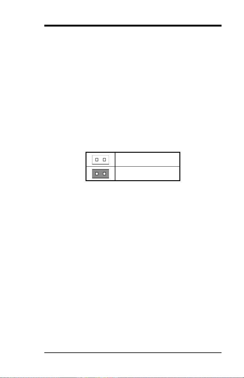
The following examples show the conventions used in this chapter.
Jumper Open
Jumper Closed/Short
MI7VGA User’s Manual 13
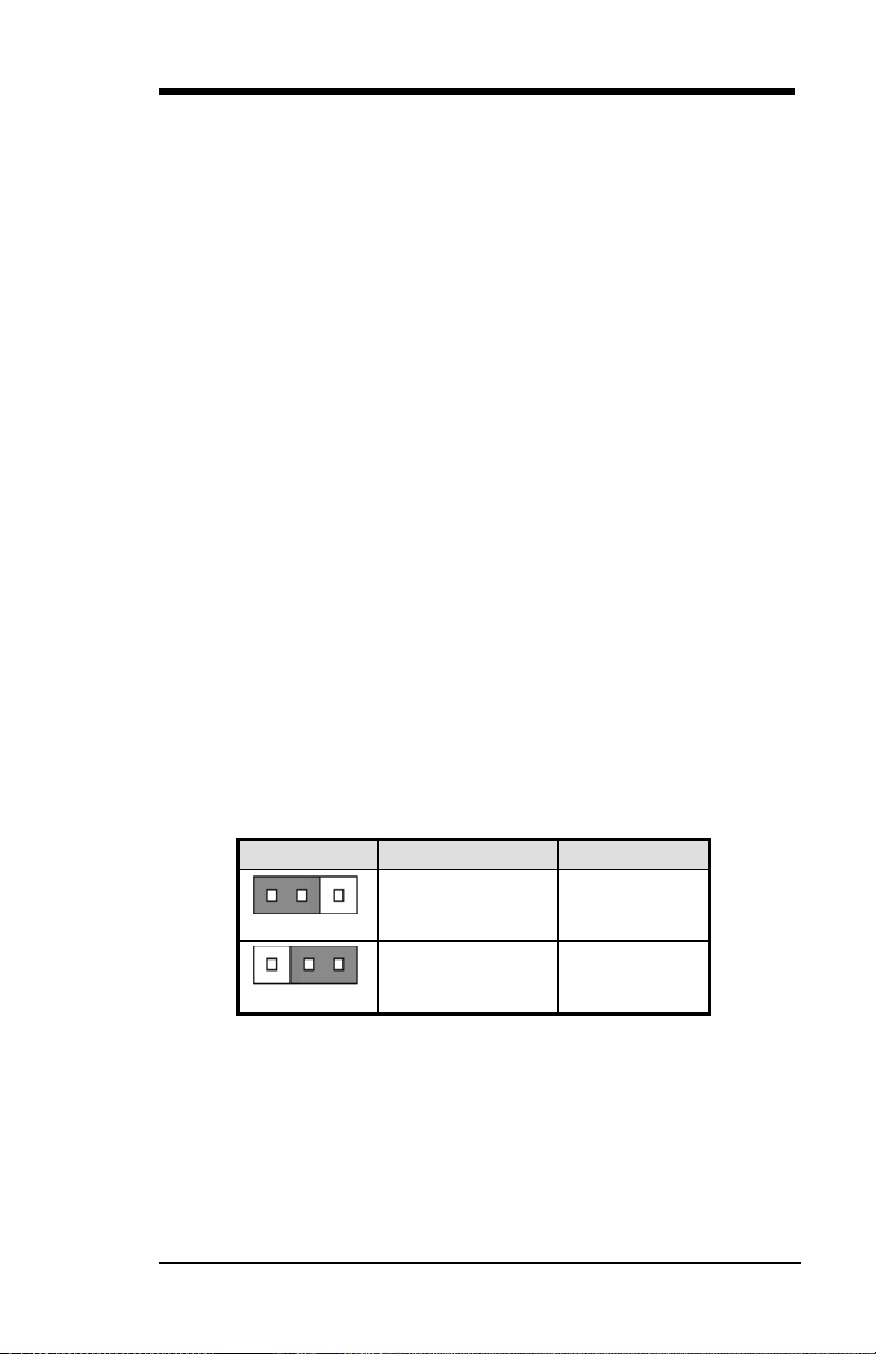
Chapter 4 Configuring the Motherboard
Figure 2: Jumper Location on the MI7VGA
14 MI7VGA User’s Manual
Chapter 4 Configuring the Motherboard
4.1 PU Frequency Setting
The M 7VGA uses jumper-free technology in configuring the
processor on the motherboard. The system automatically detects the
CPU bus speed, 66MHz or 100MHz and sets the multiplier, or ratio, to
3X. However, the bus speed can also be configured through the B OS
if the processor supports this feature. The B OS (under CPU Features
Setup) allows users to change the CPU bus speed multiplier (3X, 3.5X,
4X, 4.5X, 5X, 5.5X, 6X, 6.5X, 7X, 7.5X, 8X) to set the correct or
desired CPU frequency. The CPU bus speed multiplier will remain
unchanged if the CPU installed supports a fixed (only one) bus speed
multiplier.
IMPORTANT NOTE: t is possible that the system will not
boot if the CPU has been changed. When this happens, turn
off the computer by pressing the power button and turn it on
again by pressing the Insert key and the power button
simultaneously. (Note to press the Insert key until an image
appears on the screen.) When the system is turned on, press
the Delete key to enter B OS Setup and configure the CPU
speed.
4.2 lear MOS Select: JP5
Use JP5, a 3-pin header, to clear the contents of the CMOS RAM.
Do not clear the CMOS RAM unless it is absolutely necessary.
You will lose your password, etc.
JP5 Jumper Setting Function
1 2 3 pin 1-2: short Normal
1 2 3
pin 2-3: short Clear CMOS
NOTE: To clear CMO , the power connector should be
disconnected from the motherboard.
MI7VGA User’s Manual 15
Chapter 4 Configuring the Motherboard
4.3 JP3: SDRAM lock Select
Use JP3 to set the SDRAM clock. f the SDRAM on board is PC-
66 compatible (instead of PC-100), while your CPU bus speed is
100MHz, you have to short JP3. Failing to do so could lead to an
unstable system.
JP3 Setting Function
Open Run CPU Clock
Short Run AGP Clock
4.4 PU Host Frequency Force Selector: JP4
The M 7VGA is able to detect the host frequency (66MHz or 100MHz)
of the installed CPU. The JP4 jumper, however, can be set to OPEN to
override the detection and force the host frequency to run at 100MHz.
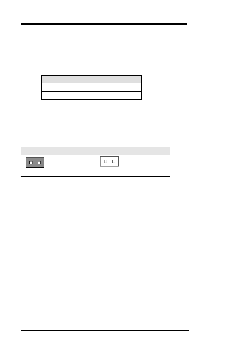
JP4 Function JP4 Function
SHORT
Host Frequency
Auto-detect
(default) OPEN
Host Frequency
set to 100MHz
NOTE: When JP4 is set to OPEN, the system may not boot or
become unstable. In such cases, return the jumper to
configure JP4 as ‘ HORT’.
16 MI7VGA User’s Manual
Table of contents
Other TMC Motherboard manuals


