TMC TI6VG4 User manual

TI6VG4
Pentium II/III Apollo Pro 133(A)
ATX Motherboard
User's Manual
Version 1.1

ii TI6VG4 User’s Manual
Copyright Notice
This publication is protected by copyright and all rights are reserved. No
part of it may be reproduced or transmitted by any means or in any form,
without prior consent of the original manufacturer.
The information in this document has been carefully checked and is
believed to be accurate. However, the original manufacturer assumes no
responsibility for any inaccuracies that may appear in this manual. In no
event will the original manufacturer be liable for direct, indirect, special,
exemplary, incidental, incidental or consequential damages resulting
from any defect or omission in this manual, even if advised of possibility
of such damages. The material contained herein is for informational
purposes only.
Acknowledgments
Award is a registered trademark of Award Software International, Inc.
IBM, PS/2 are trademarks of International Business Machines
Corporation.
Intel and Pentium are registered trademarks of Intel Corporation.
Apollo Pro is a trademark of VIA Technologies.
Microsoft Windows is a registered trademark of Microsoft Corporation.
All other product names or trademarks are properties of their respective
owners.

Contents
TI6VG4 User’s Manual iii
Contents
Chapter 1 Introduction....................................................1
Chapter 2 Specifications..................................................3
Chapter 3 Hardware Description ...................................5
3.1 Processor ...................................................................................7
3.2 L2 Cache ...................................................................................7
3.3 Main Memory............................................................................7
3.4 BIOS..........................................................................................9
3.5 Onboard AGP Slot.....................................................................9
3.6 Hardware Monitoring................................................................9
3.7 Multi-I/O ...................................................................................9
3.8 Interrupt Request (IRQ) Lines.................................................10
3.9 Onboard PCI-IDE....................................................................10
3.10 DMA Channels......................................................................10
3.11 I/O Port Address Map............................................................11
3.12 Onboard Audio......................................................................11
3.13 AMR Slot ..............................................................................11
Chapter 4 Configuring the Motherboard ....................13
4.1 CPU Frequency Setting ...........................................................15
4.2 JP4, JP5: Force Clock Select...................................................15
4.3 JP6: Onboard Audio and AMR Slot Setting ...........................16
4.4 JP9: Clear CMOS Select .........................................................16
Chapter 5 Installation....................................................17
5.1 I/O Connectors ........................................................................19
5.2 J1: PS/2 Keyboard and PS/2 Mouse Connectors.....................19
5.3 J2: ATX Power Supply Connector..........................................20
5.4 J5: Floppy Drive Connector ....................................................20
5.5 IDE1, IDE2: EIDE Connectors...............................................21
5.6 J3, J6: Serial Ports...................................................................23
5.7 J4: Parallel Port Connector......................................................23
5.8 J10, J7, J8, J9: Game Port, Mic In/Line In/Line Out...............24
5.9 J12, J13, J14: CD In and Auxiliary In Connectors.................24
5.10 FAN1, FAN2, FAN3: Fan Power Connectors.......................24
5.11 J16: IrDA Connector .............................................................25
5.12 USB1, J18: USB Connectors.................................................25

Contents
iv TI6VG4 User’s Manual
5.13 J15: Wake on LAN Connector...............................................25
5.14 J17: Front Bezel Connectors..................................................26
Chapter 6 BIOS Configuration.....................................28
6.1 BIOS Introduction ...................................................................31
6.2 BIOS Setup..............................................................................31
6.3 Standard CMOS Setup.............................................................33
6.4 BIOS Features Setup................................................................36
6.5 Chipset Features Setup.............................................................40
6.6 Power Management Setup .......................................................43
6.7 PNP/PCI Configuration ...........................................................46
6.8 Load BIOS Defaults ................................................................48
6.9 Load Setup Defaults.................................................................48
6.10 CPU Speed Setting ................................................................49
6.11 Integrated Peripherals............................................................51
6.12 Supervisor / User Password...................................................53
6.13 IDE HDD Auto Detection......................................................54
6.14 Save & Exit Setup..................................................................55
6.15 Exit Without Saving...............................................................55
Chapter 7 VIA Drivers Installation Guide ..................56
7.1 Windows 98 4-in-1 Driver Installation....................................56
7.2 Windows 98/95 DirectX Installation.......................................59
7.3 Windows 98 Audio Driver Installation....................................61
7.4 Windows 98SE 4-in-1 Driver Installation................................62
7.5 Windows 98SE Audio Driver Installation ...............................64
7.6 Windows 95 4-in-1 Driver Installation....................................65
7.7 Windows 95 Audio Driver Installation....................................70
7.8 Windows NT 4.0 Audio Driver Installation.............................71
Appendix..........................................................................75
A. Slot 1 Retention Mechanism......................................................75
Additions & Errata.........................................................76
Chapter 1 Introduction
TI6VG4 User’s Manual 1
Chapter 1 Introduction
This manual is designed to give you information on the TI6VG4
motherboard. It is divided into the following sections:
•
••
•
Introduction
•
••
•
Specifications
•
••
•
Hardware Description
•
••
•
Configuring the Motherboard
•
••
•
Installation
•
••
•
BIOS Configuration
•
••
•
VIA Drivers and DirectX Installation
Checklist
Please check that your package is complete and contains the items below.
If you discover damaged or missing items, please contact your dealer.
The TI6VG4 Motherboard
1 IDE ribbon cable
1 floppy ribbon cable
1 CD containing a system monitoring utility, Bus Master IDE
driver and utilities.
Product Information
TI6VG4 TI6VG4X
Chipset 82C693AA 82C694X
AGP 2X 2X/4X
* After installing Windows 95 or Windows 98(SE), install VIA 4 in 1
drivers to ensure that your system works properly.

Chapter 1 Introduction
2TI6VG4 User’s Manual
This page was intentionally left blank.

Chapter 2 Specifications
TI6VG4 User’s Manual 3
Chapter 2 Specifications
The TI6VG4 is a high-performance ATX Apollo Pro 133(A)
motherboard with a Slot 1 connector for PentiumII/III processors. It
offers flexibility in terms of CPU frequency and main memory type and
size. The main features of the motherboard consist of the following:
CPU Socket
Slot 1
Processor
Intel Pentium II 233/266/300MHz (66MHz / Klamath)
Intel Celeron 266/300/300A/333 (66MHz)
Intel Pentium II 333MHz (66MHz / Deschutes)
Intel Pentium II 300/350/400/450MHz (100MHz / Deschutes)
Intel Pentium III 450/500/550MHz (100MHz / Katmai)
Intel Pentium III 533/600/667MHz (133MHz / Katmai/Coppermine)
L2 Cache
CPU integrated L2 cache
Main Memory
Three 168-pin DIMM sockets with PC133 support
Memory types: Extended Data Output (EDO) DRAM, SDRAM
(Synchronous DRAM)
Memory size: 16MB, 32MB, 64MB, 128MB, 256MB, 512MB
Chipset
VIA Apollo Pro 133(A) (VT82C693AA/X and VT82C686A)
Super I/O
The super I/O is a built in the VT82C686A chip and supports:
z
Two 16550 UART compatible serial ports
z
One parallel port (ECP/EPP compatible)
z
One floppy controller (2.88MB compatible)
z
One IrDA port
PCI Bus Master IDE Controller (UDMA33/66)
Onboard PCI Bus Master IDE (UDMA33/66) controller with two
connectors for up to four IDE devices in two channels, supporting
faster data transfer rates, enhanced IDE devices, PIO Mode 3/4 and
Bus Mastering Ultra DMA33/66 (You have to install the Bus Master
IDE driver to enable this feature.)

Chapter 2 Specifications
4TI6VG4 User’s Manual
BIOS
Award BIOS with ISA Plug and Play (PnP) extension, DMI, bootable
CD-ROM and power-management features. The BIOS is Y2K (Year
2000) compliant.
Mouse Connector
PS/2 type
Keyboard Connector
PS/2 type
USB Connector
One external stacked USB connector with 2 ports and a pin-header
connector for the optional USB connector to support another 2 ports.
Windows 98/95-shut-off
Allows shut-off control from within Windows 98/95
Onboard Audio
The AC-97 audio function is integrated in the VIA VT82C686A South
Bridge chip.
Onboard AGP Slot
The AGP (Accelerated Graphics Port) slot supports AGP compliant
VGA cards to achieve rich 3D and video graphics display.
VT82C693AA supports 2X AGP while VT82C694X supports 2X/4X
AGP.
Expansion Slots
Five 32-bit PCI slots
One 16-bit ISA slots
One AGP slot
One AMR slot for a modem riser card
Form Factor
ATX, 12” x 7.48 (30.5cm x 19cm)

Chapter 3 Hardware Description
TI6VG4 User’s Manual 5
Chapter 3 Hardware Description
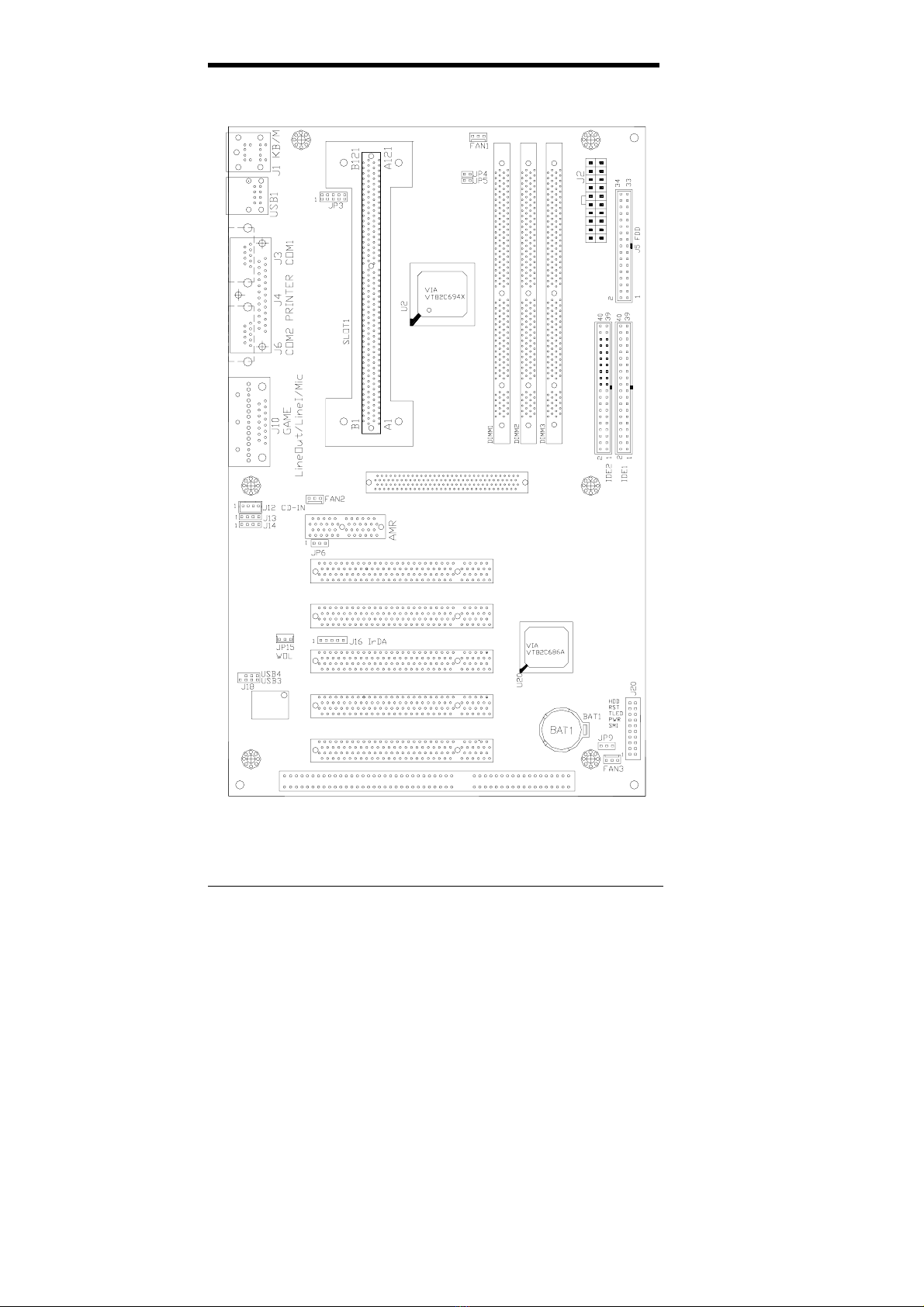
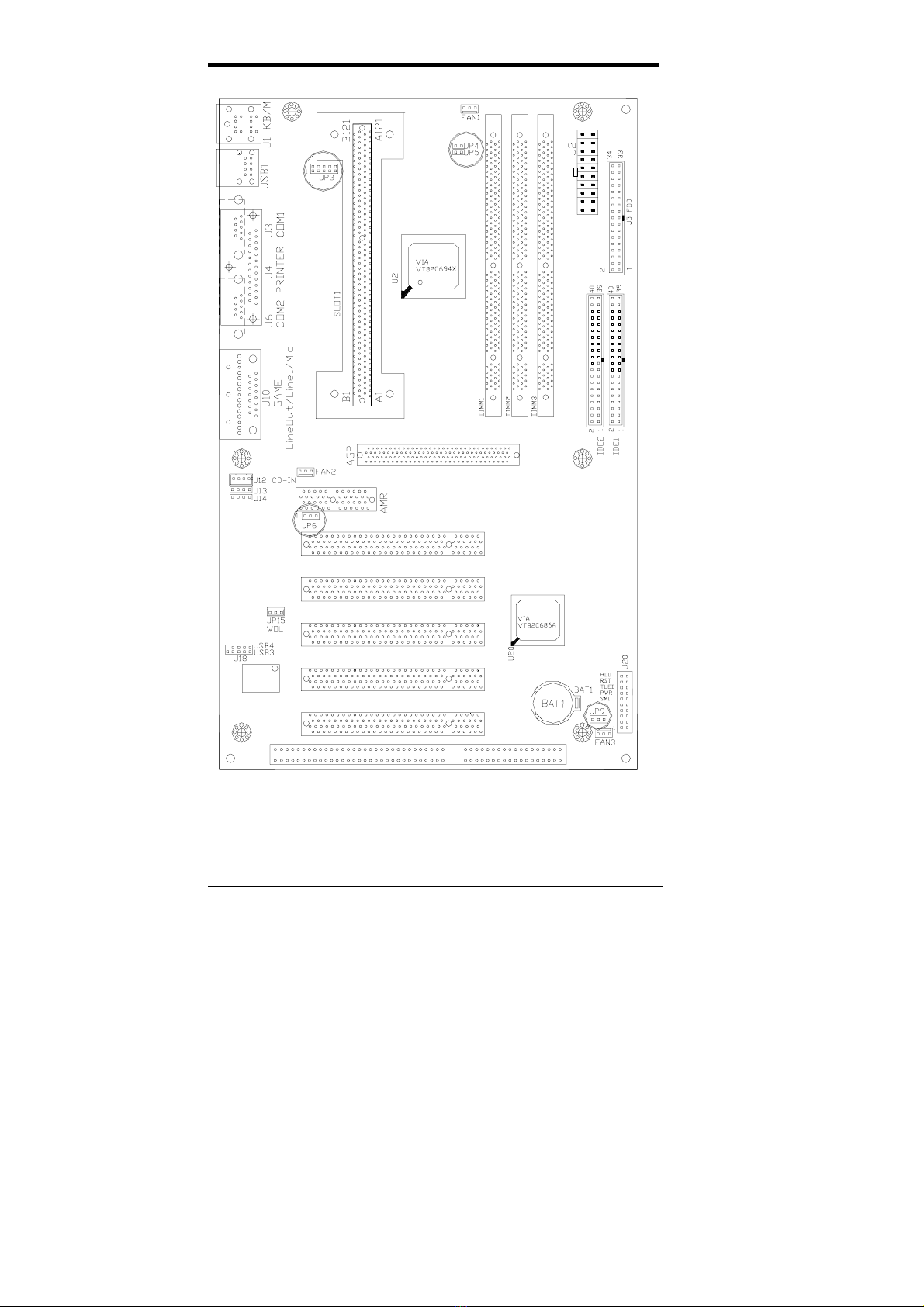
This chapter briefly describes each of the major features of the TI6VG4
motherboard. The layout of the board in Figure 1 shows the location of
the key components. The topics covered in this chapter are as follows:
3.1 Processor ...................................................................................7
3.2 L2 Cache ...................................................................................7
3.3 Main Memory............................................................................7
3.4 BIOS..........................................................................................9
3.5 Onboard AGP Slot.....................................................................9
3.6 Hardware Monitoring................................................................9
3.7 Multi-I/O ...................................................................................9
3.8 Interrupt Request (IRQ) Lines.................................................10
3.9 Onboard PCI-IDE....................................................................10
3.10 DMA Channels......................................................................10
3.11 I/O Port Address Map............................................................11
3.12 Onboard Audio......................................................................11
3.13 AMR Slot ..............................................................................11
Chapter 3 Hardware Description
6TI6VG4 User’s Manual
Figure 1: Layout of the TI6VG4 Motherboard
Chapter 3 Hardware Description
TI6VG4 User’s Manual 7
3.1 Processor
The TI6VG4 motherboard is designed to take an Intel Pentium II/III
processor running 233/266/300/333/350/400/450/500/533/550/600/
667MHz or an Intel Celeron processor running 266/300/333/366
/400/433/466MHz with its Slot 1 processor connector.
3.2 L2 Cache
The L2 cache is integrated in the processor.
3.3 Main Memory
The TI6VG4 motherboard supports three 168-pin DIMM (Dual In-line
MemoryModule) sockets to forma memory configuration from 16MB to
1.5GB. DIMM modules can be 16MB, 32MB, 64M, 128MB, 256, and
512MB in SDRAM. In populating the DIMM sockets, any socket can be
populated first. Refer to the following table on how to do the memory
configuration.
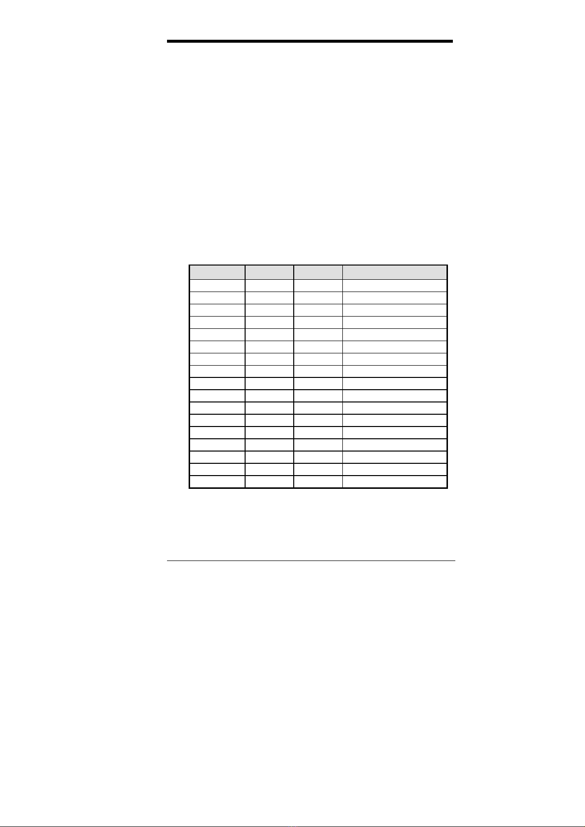
(DIMM1) (DIMM2) (DIMM3) Total Memory
16MB ----- ----- 16MB
32MB ----- ----- 32MB
64MB ----- ----- 64MB
128MB ----- ----- 128MB
16MB 16MB ----- 32MB
32MB 16MB ----- 48MB
64MB 16MB ----- 80MB
128MB 16MB ----- 144MB
16MB 16MB 16MB 48MB
32MB 16MB 16MB 64MB
64MB 16MB 16MB 96MB
128MB 16MB 16MB 160MB
32MB 32MB ----- 64MB
64MB 32MB ----- 96MB
128MB 32MB ----- 160MB
32MB 32MB 16MB 80MB
64MB 32MB 16MB 112MB
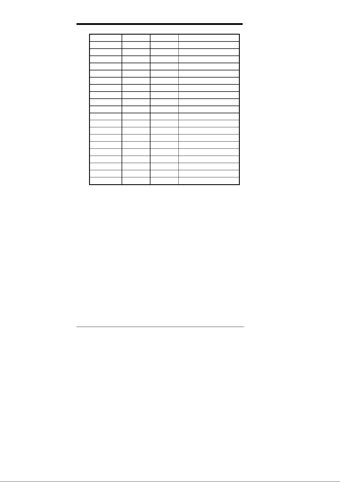
Chapter 3 Hardware Description
8TI6VG4 User’s Manual
128MB 32MB 16MB 176MB
32MB 32MB 32MB 96MB
64MB 32MB 32MB 128MB
128MB 32MB 32MB 192MB
64MB 64MB ----- 128MB
128MB 64MB ----- 192MB
64MB 64MB 16MB 144MB
128MB 64MB 16MB 208MB
64MB 64MB 32MB 160MB
128MB 64MB 32MB 224MB
64MB 64MB 64MB 192MB
128MB 64MB 64MB 256MB
128MB 128MB 128MB 384MB
256MB 256MB
256MB 128MB 128MB 512MB
256MB 256MB 512MB
256MB 256MB 256MB 768MB
512MB 512MB
512MB 512MB 1GB
512MB 256MB 256MB 1GB
512MB 512MB 512MB 1.5GB
Notes:
z Memory modules specified for the motherboard are 168-pin
SDRAM DIMMs and all sizes may be currently available.
z Other DIMM combinations may also result in the same totals.
z This is not an exhaustive list of possible combinations.
z With 133MHz bus speed, use SDRAM modules with PC133 or
PC100 specification. When using 100MHz bus speed, use SDRAM
modules with PC133/100/66 specification. When using 66MHz bus
speed, use SDRAM modules with PC100 or PC66 specification.

Chapter 3 Hardware Description
TI6VG4 User’s Manual 9
3.4 BIOS
The BIOS on the TI6VG4 motherboard provides the standard BIOS
functions plus the following additional features:
1. ISA Plug and Play (PnP) Extension
Unlike PCI cards that are Plug and Play, ISA cards require setting
jumpers to resolve hardware conflicts. To make a computer system
PnP, an ISA PnP standard is established and supported by new
operating systems, such as Windows 95. Under Windows 95, the
motherboard BIOS must have an ISA PnP extension to support new
ISA PnP cards.
2. Power Management
The power management feature provides power savings by slowing
down the CPU clock, turning off the monitor screen and stopping the
HDD spindle motor. The BIOS fully conforms to ACPI (Advanced
Configuration and Power Interface) specification.
3.5 Onboard AGP Slot
The AGP (Accelerated Graphics Port) slot supports AGP compliant
VGAcards to achieve rich 3D and video graphics display. VT82C693AA
supports 2X AGP while VT82C694X supports 2X/4X AGP. AGP is a
platform bus specification that enables 3D graphics capabilities including
support for z-buffering, alpha blending and faster texture mapping.
3.6 Hardware Monitoring
Hardware monitoring is integrated in the VIA VT82C686A South Bridge
chip. It monitors your PC’s voltage, temperature and fan speeds to ensure
a more stable computer system. This feature is compatible with the
System Monitor utility.
3.7 Multi-I/O
The motherboard’s multi-I/O is integrated in the VIA VT82C686A South
Bridge supports a keyboard controller, two serial ports, one parallel port,
one floppy controller and one IrDA port. The serial ports are 16550
UART compatible. The parallel port features high-speed EPP/ECP
mode. The floppy controller supports up to 2.88MB format.
Chapter 3 Hardware Description
10 TI6VG4 User’s Manual
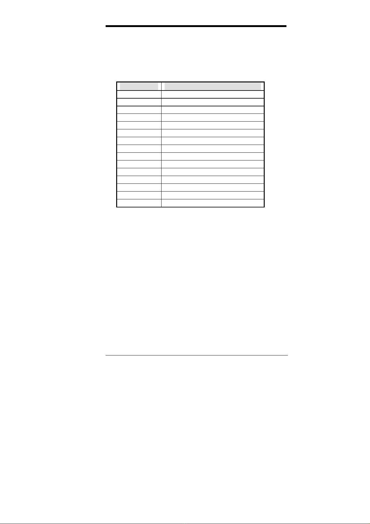
3.8 Interrupt Request (IRQ) Lines
There is a total of 15 IRQ lines available on the motherboard. Peripheral
devices use an interrupt request to notify the CPU for the service
required. The following table shows the IRQ lines used bythe devices on
the motherboard:
Level Function
IRQ0 System Timer Output
IRQ1 Keyboard
IRQ2 Interrupt Cascade
IRQ8 Real Time Clock
IRQ9 Software Redirected to Int 0Ah
IRQ10 Reserved
IRQ11 Reserved
IRQ12 Reserved
IRQ13 Co-Processor
IRQ14 Primary IDE
IRQ15 Secondary IDE
IRQ3 INTERRUPT
IRQ4 Serial Port #1
IRQ5 INTERRUPT
IRQ6 Floppy Disk Controller
IRQ7 Parallel Port #1
3.9 Onboard PCI-IDE
The PCI-IDE controller, integrated in the VIA chipset, supports PIO
mode 3/4 and bus mastering Ultra DMA33/66. Using HDDs that support
Ultra DMA33/66, hard drive data transfer speed is increased for better
overall system performance. There are two IDE connectors - primary
IDE and secondary IDE. With two devices per connector, up to four IDE
devices can be supported.
3.10 DMA Channels
There are seven DMA channels available on the motherboard. Only
DMA2 is used by the floppycontroller. In the case that ECP mode on the
parallel port is utilized, DMA1 or DMA3 will be used.
Chapter 3 Hardware Description
TI6VG4 User’s Manual 11
3.11 I/O Port Address Map
Each peripheral device in the system is assigned a set of I/O port
addresses which also becomes the identity of the device. There is a total
of 1K port address space available. The following table lists the I/O port
addresses used on the motherboard.
Address Device Description
000h - 01Fh DMA Controller #1
020h - 03Fh Interrupt Controller #1
040h - 05Fh Timer
060h - 06Fh Keyboard Controller
070h - 07Fh Real Time Clock,, NMI
080h - 09Fh DMA Page Register
0A0h - 0BFh Interrupt Controller #2
0C0h - 0DFh DMA Controller #2
0F0h Clear Math Coprocessor Busy Signal
0F1h Reset Math Coprocessor
1F0h - 1F7h IDE Interface
2F8h - 2FFh Serial Port #2(COM2)
378h - 3FFh Parallel Port #1(LPT1)
3F0h - 3F7h Floppy Disk Controller
3F8h - 3FFh Serial Port #1(COM1)
3.12 Onboard Audio
The AC-97 audio is integrated in the VIA VT82C686A South Bridge
chip. It features high quality PC audio with surround sound to bring new
levels of realism to games and eliminates audio card non-compatibility
issues.
3.13 AMR Slot
The AMR slot on the TI6VG4 motherboard is designed to support an
AC-Link compatible modem riser card. The audio function is already a
built-in feature of the motherboard.

Chapter 3 Hardware Description
12 TI6VG4 User’s Manual
This page was intentionally left blank.
Chapter 4 Configuring the Motherboard
TI6VG4 User’s Manual 13
Chapter 4 Configuring the Motherboard
The following sections describe the necessary procedures and proper
jumper settings to configure the TI6VG4 motherboard. For the locations
of the jumpers, refer to Figure 2.
4.1 CPU Frequency Setting ...........................................................15
4.2 JP4, JP5: Force Clock Select...................................................15
4.3 JP6: Onboard Audio and AMR Slot Setting ...........................16
4.4 JP9: Clear CMOS Select .........................................................16
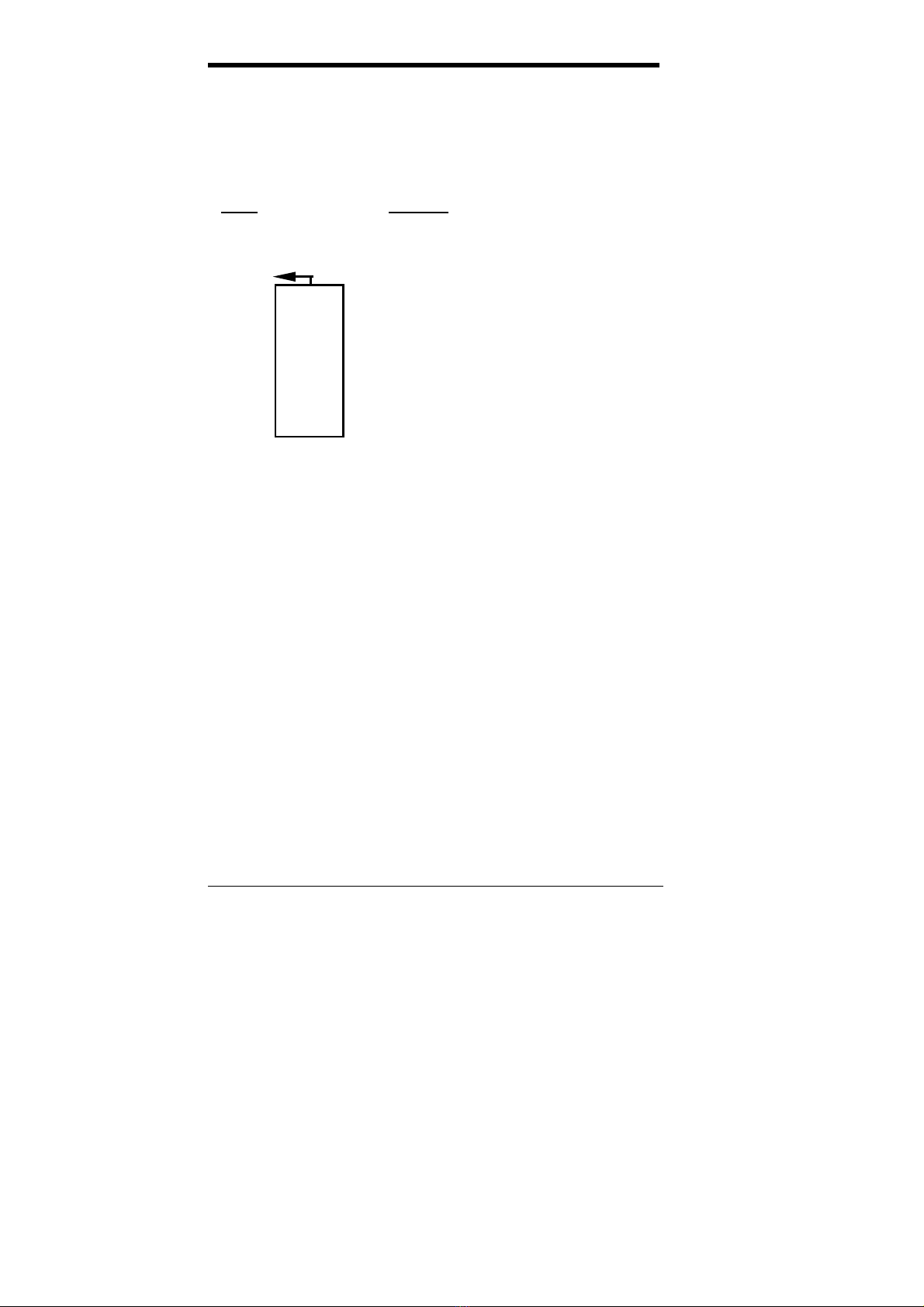
The following examples show the conventions used in this chapter.
Jumper Open
Jumper Closed/Short
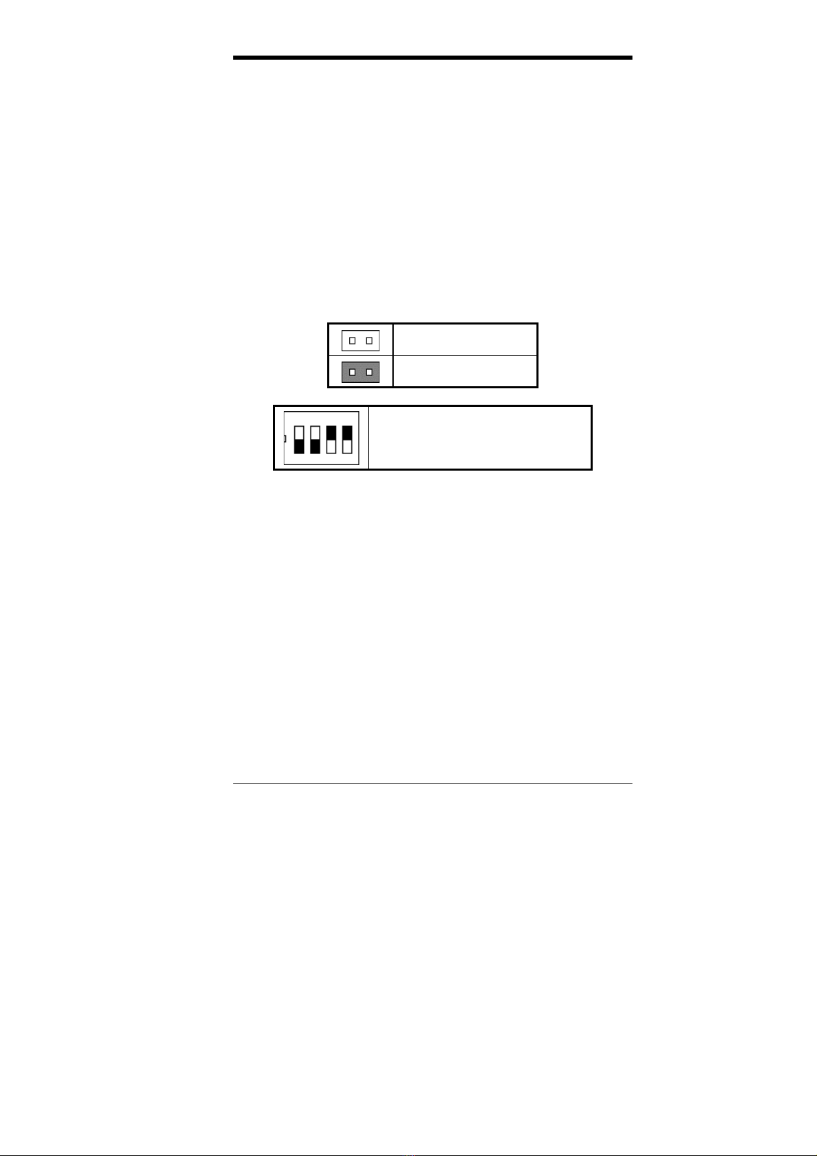
Switch 1 and switch 2 are set to OFF.
Switch 3 and switch 4 are set to ON.
CAUTION: Danger of explosion if battery is incorrectly replaced.
Replace only with the same or equivalent type
recommended by the manufacturer.
1 2 3 4
DIP
ON
Chapter 4 Configuring the Motherboard
14 TI6VG4 User’s Manual
Figure 2: Jumper Location on the TI6VG4
Chapter 4 Configuring the Motherboard
TI6VG4 User’s Manual 15
4.1 CPU Frequency Setting
The TI6VG4 uses jumperfree technology in configuring the processor on
the motherboard. The system automatically detects the CPU bus speed,
66MHz, 100MHz or 133MHz and sets the multiplier, or ratio, to 3X. The
maximum multiplier is 8X. The BIOS (under Chipset Feature Setup)
allows users to change the CPU multiplier to set the correct or desired
CPU frequency.
IMPORTANT NOTE: It is possible that the system will not
boot if the CPU has been changed. When this happens, turn off
the computer by pressing the power button and turn it on again
by pressing the Insert key and the power button
simultaneously. When the system is turned on, press the Delete
key to enter BIOS Setup and configure the CPU speed.
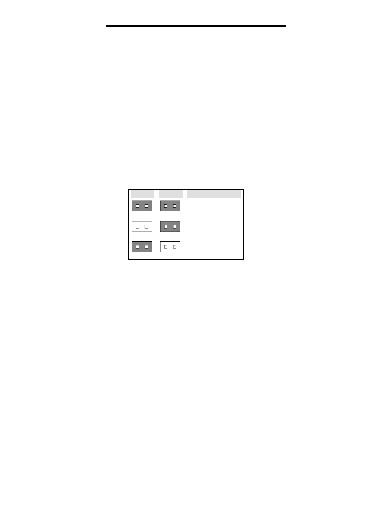
4.2 JP4, JP5: Force Clock Select
Use these two jumpers to force the CPU bus speed (FSB) from
66MHz to 100MHz or from 100MHz to 133MHz. Refer to the
table below on how to configure the jumper.
JP4 JP5 Bus Speed / FSB
short
short
Normal
open
short
Force 66MHz to
100MHz
short
open
Force 100MHz to
133MHz

Chapter 4 Configuring the Motherboard
16 TI6VG4 User’s Manual
4.3 JP6: Onboard Audio and AMR Slot Setting
JP6 Setting Onboard Audio AMR
1 2 3
Pin 1-2
: short Primary Secondary
1 2 3
Pin 2-3
: short Secondary Primary
4.4 JP9: Clear CMOS Select
Use JP9, a 3-pin header, to clear the contents of the CMOS RAM.
Do not clear the CMOS RAM unless it is absolutelynecessary. You
will lose your password, etc.
JP9 Jumper Setting Function
1 2 3
pin 1-2: short Normal
1 2 3 pin 2-3: short Clear CMOS
NOTE:To clear CMOS, the ATX-power connector should be
disconnected from the motherboard.
Table of contents
Other TMC Motherboard manuals


