Uniden UH001 User manual

ServiceMamuail
UHF CB/FM O-CHANNEL
MOBILE TRANSCEIVER
uniden'
CONTENTS
Spcc i.al ons . . 2
0 sasse$b y nsirucl .:l
tsackDagranr ... .. 5
A g.n€ni Proceaure
iro!b !shool ng tsinis
... 6
if
PCB {Top and BotloD ! efrs) ]E
ll/ir fl D.!.nn] 2i
E eclrl.a Paflsl sl .21
Erp oded V ew 35
N'i.char cal Pa.ls Lisi .. 3.q
vora!c chart
5i
5€,od o, d '
tl
v
A
tl
tr
v
lC nlerr.l O agranrs
Schcnratic Diagranr

GENERAL
Channels
Irequency Range
Crystal Osci ator
tM lcro p ho ne
Speaker
Antenna Connector
Jacks & Connectofs
Contro s
lliu.ninaiions
Cabinet S ize
Welght
SPECIFICATIONS
40
416.125 MNz ro 411.400 f,lHz lSee page I3. FREOUENCYCHART)
. REPEATER USE (CF 1 ro Cl.l 8, TX only):
411 .115 MHz ta 4ll.350 MNz
600 ohrn, Dynamic Type
B ohnr, 3W
tM Type
Mlc 4P i\,l€tal
EXT SP 3.5{,
DC Powe.3P Type
Chanfel Se ecto., Power Switch & Volume, Sque ch,
Tone SO Switch, Tone Ca l Switch, Dupiex S\ rlrch
Channel Readout (LED)
TX lndlcator (LED)
RX Indicator lLE D)
W: 5 "/3,' {150mm)
H: 1-31/3," (50mm)
D: 7-"/61" T 90mm
3.s3 bs (1.6 Kg)
DC Do^o .ab " ^ BL, I i. Vi. opi,o,e
[.4jcrophone H: ngei
MEASU R EIM ENT CONDITIONS
Power Source
A|]tenna lmpedance
Test Temperature
lv4odu latl on Frequ ency
l\4ean Signal Inp!t Level
Refefence Audio Output Power
Ref€rence ivlodulatlon Devlatlon
Audio Output Lead
T 3.8V (DC)
50 ohm
11"F (2s'C)
l kHz (R X/IX)
1000pV
500mW
3 kHz Deviat on
8 ohm res stlvc
TRANSl\4ITTE R SECTION
Frequency Tolerance at 77'F (25'C)
{5 Fninutes after switch on}
Carrler Power
Spurlous Emisslon
416.3625 MNz @ 411 .4625 MHz
476.3125 UHz to 476.3625 MFlz
477.4625 MHz rc 411.5125 MHz
Other Frequency
Current Drain
[.4odulat]or] Frequency Fesponse
(1 kHz,0 dB reference, at 600 Hz devlarion)
Lower at 500 Hz
Upper at 2-5 kHz
Microphone Sensitivity for 3 kHz Deviation
f\4aximum Deviation at 1 kHz
at 6 kHz
UNIT NOMINAL LIMIT
kHz 10.5 !2.5
W 5 3.5io6
pW -- 2AO
!w 2.5
/rW 25
lrvv - l
mA 1300 2000
dB 6 -3to-g
dB +8 +5to+11
mV 3 6
kHz !4.75 13.5 to r5
-2
kHz Less than 11 .5

R ECE IVE B SECTION
Sensitivlty for 12 dB S/N
Overall Audlo Fidelity (1 kHz,0 dB re{erence)
Lower at 500 Hz
Upper at 2.5 kHz
Adjacent Channe Selectivity (125 kHz)
N4aximum ALrdio Output Power
Audio Output Povver at 10% THD
Hum & Noise Ratio at Input lmV
Sque ch Sensitivlty at Threshold
Sque ch Sensitivity at Ti€ht
lmage Rejectlon Ratio
F Rejection Ratio
Oscillator DropoLrt Voltage
Cr-rrrent Drain at No Signa
Current Drain at l\4aximum Output
UNIT
dB
dB
dB
dB
dB
dB
+3
-8
55
3
2
40
0.25
1
60
90
I
300
800
0to+B
4 ro -12
45
2
'1 .5
30
1.0
0.5 to 2
40
60
11
450
1240
NOMINAL LIMIT
0.25 0.5
NOTE: Nominal specs represent the design specs. A I units should be able to approximate thes3
some !\rl I exceed and some may drop sllghtly below these specs. Limit specs represent the absotute
worst condition that stil might be considered acceptable; in no case should a Lrnit per{orm to ess than
anv lrmtl spec,
-3-

BLOCK DIAGRAM
v
.5
I il
l!:
LJl
-/"r- {
ET
tie
F:
i

ALIGI\IMENT PROCEDURE
r:1i*:.
I .)r,
,t.f '
r ie,
. :.;.,
:;::*B]jr
ffi
i,.?*;l
Lii'5 '
J,LJ
o;*::
. . .:1,::. !
'' r[e]l;,
i "rO 6;= r
'. .@-;'";'
"i''{$a.ir!
;. ,r' -l .i^ir- l
' _ i'_ :-"-
-6-

LOCAL FREQUENCY ALIGNMENT
(RCfEr tO AL IG NI\,1ENT POINTS)
'i. Test Equipment Required
a. Oscilloscope {0 \ 50 MHz)
b. DC Power SLrpp y (13.8V/2AJ
c. DC Vo tmeter (10V maxlmunr, 10k ohm/V)
d. Frequency Counter (0 a 200 I\4Hz)
e. 50 ohrn Load and Attenuator
2- Alignment Procedure
STEP BESET TO ADJUSTMENT REMABKS
CH:40 L24 Conoect DC voltmerer to or oscil oscope to
TPl. Adlu( for 3 0V re:dlns.
2CH:40 L2l Connecl osciloscope io TP2.
Adjust lor maximum anrpl lude.
3CH:40 Ll0 Co.nect lreq!eicy counler to TP2.
Adjust for €adi.! ol 152.0 tvlHz 150 H:
Note: Voltage atTPl shouLd be higherthan 2V in TX mode at CHl, and 1 a 4_5V in RX mode ar
channes 1 ! 40.
3. Test Equipment Connection
-7-

TRANSMITTEB ALIGNMENT
{REfEr tO ALIGNMENT POINTS)
'l- Test Equipment Required
a. DC Power Supply (13.8V/2A)
b. DC Voltmeter (1V DC/FullScale)
c. R F Output Power l\4eter
d. f.oquancy Co-nrer l0 200 Ml,,)
e AF Voltmeier
f. 50 ohm Load and Attenuator
g. Audio Oscillator
h Linear Detector
2. Alignment Procedure
STEP PRESET TO AOJUSTMENT REMARKS
CH: 20
RT5: Vlax.
CTI:Ce.ter
CTz: Center
FT5 Connect DC voltmeter to TP4. Adj!st for
max. amplitude. (Bepeat two limes)
2Connect BF power meter to ANT. Termlnal.
Aclj!st ior max. power. {Repeat two times)
cTl Adjust powerto5.0W wiih CT1, roizlins in
di.ectlon which increases capacity.
129 Connect fr€quency co!nter. Adjust for anten
na frequency of 476.90 l\/Hz 1150 Hz.
30mV I kHz Connect linear detector to ANT. termiia
Adjost to obtain deviation of 14.7 kHz.
Note: RT5 adjustment is reqLrired only when the CTCSS module is installed.
3. Test Equipment Connection
$
8

RECEIVER ALIGNMENT
(Refer to ALIGNI4ENT POTNTS)
1. Test Equipment Required
". Ol illosLopp (0 50 VH7)
b. DC Power Supply (13.8V/2A)
c. RF Signa Generaior
(470 MHz band, 1000 Hz, 13 kHz FM Modutation,
d. AF Voltmeter
e. Dummy Load (B ohm,5W Fesistlve)
Alignment Procedure
Output lmpedance 50 ohrn)
STEP PBESET TO ADJUSTMENT B EI\,1A8 KS
VOL: N4;x.
SO: r.4 n.
CH:20 L6
Co.nect SSG (476.900 llHz) io ANT. Tem na, dno
AF Voltm.tef 10 EXT. SP Jlck.
Adjust L6 Ior max. o!tput. Temporarity roiate L6
so rhat cofe s flrrsh wlih top of cot bobbin,then
fotate it co!.terclockwjs€ fof max, ourpLrl.
2Keep ANT. input so rhar li
provides always s/N of 12 dB. Fr 1,2, 6,
13,4,5 AdlLrsl to oblain the besl S/N.
3Adjusi RTl 50 rhar rhe squel.h j!sr breaks
3. Test Equipment Connection
3tl
AF VOLTMETER OSCILLOSCOPE
-9-

PLL CIRCU IT
YES
YES YES
YES YES
YES GOOD
P LL not def€ctlve.
YES
No good
Check whether there is R F
Voltage on pin 2 of lC9.
Check whether there is aPProx.
2.5V at CH1 (RX) and 3V at
40CH lTX) on TP1.
Check whether there is F F
Vo taqe on Collector of
TR29.
ne.rlqn L14.
Defective TR27, TR2B or
poor soldering.
Check whether there is aPProx-
2.5V at CH1 (R X) and 3V at
40CH (TX) on TPl
Check whethe. voltage
reading on collector of
TR29 is approx. 7V. Check whether each channel
freqLrency rnatches the frequency
indlcated in frequencY chart-
Defectlve X'tal X3
(TX), X4 (R X) or
poor sol0erlng.
Defective Vcc
line (7.5V).
Check whether channel Programs
on Pins T 0 thru 17 of log are as
specified in the chart.
Defectlve 1C7, ICB-
Rota.y Switch or Poor
soldering.
Check whether there is R F Volt
age on Pin 4 ot lcg (8 533 MHz).
Defective ICg or Poor
soldering.
Defectlve X'tal X2 or
TROUBLESHOOTING HINTS

UNIT WILL NOT TURN ON. DOES NOT TRANSMIT,
1. Blown fuse 1 . Defective microphone jack.
2. Defective power switch. 2. Defective PTT switch on microphone.
3. Defect in power suppLy circuitry. 3. l-Jnlocked PLL circuitry of improper alignment.
DOES NOT RECEIVE SOUND. NO TX MODULATION.
1. Defective external speaker jack. 1. Defective micfophone and/or clrcu try.
2. Bad PTT switch in the microphone. 2. Defect in nrodu ation circLr try.
3. Un ocked PLL circuitry or improper a ignment.
4. Defect in squelch clrcuilry.
5. Defective Tone squelch switch.
ADDITIONAL HINTS
DOES NOT TRANSIM IT.
A. Connect the current meter ln series with power cable and check the current reading lor transrnlt mode.
lf the current reads more than 0.8A (but less than 24) t rneans the t nal o!tput transisto. is OK, so
check for bad contacts or short circults P.C. Board and Antenna Connector. lf the current reads less
than 0.5A, it lndicates there is no drive to fina t.ansistor,socheckdriveorcarlyRFstage
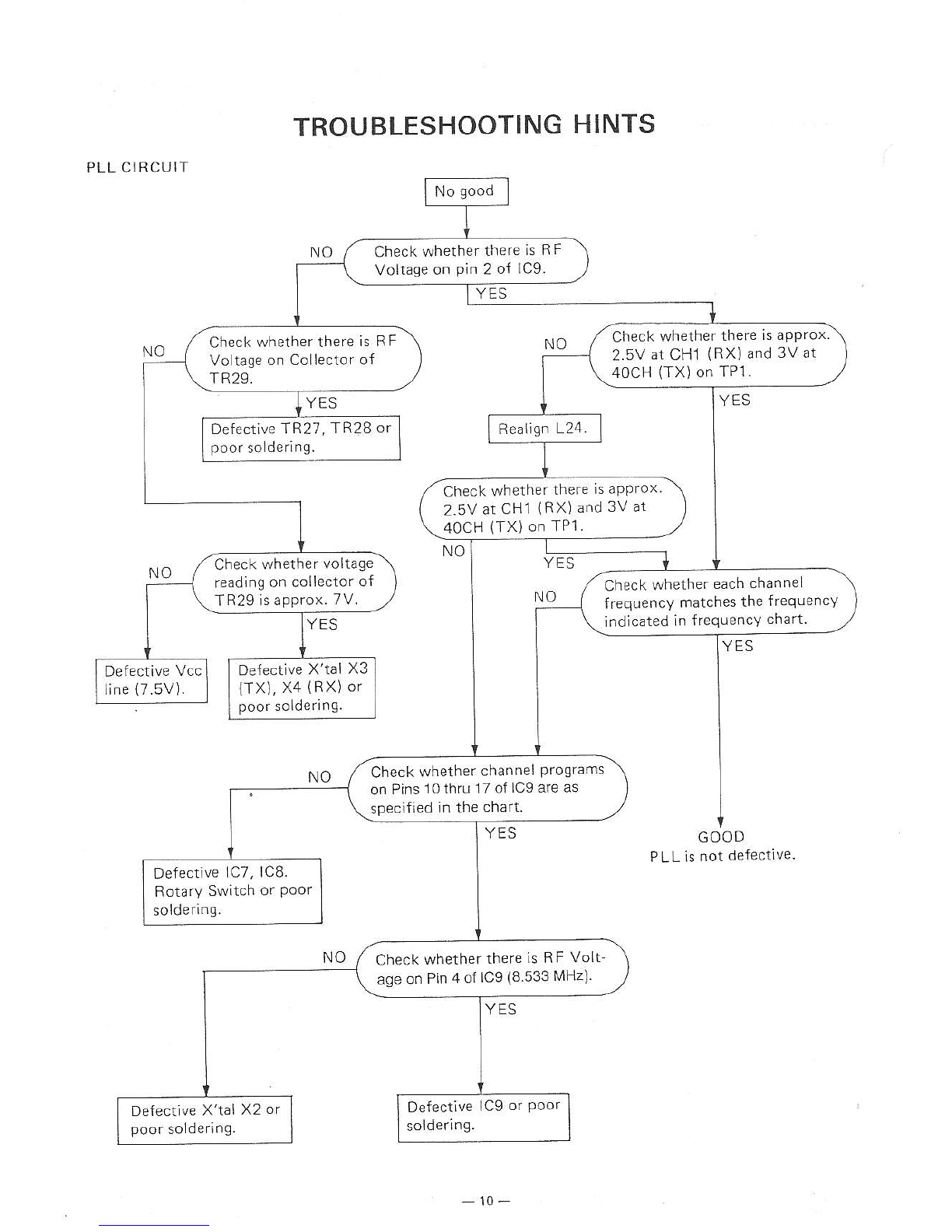
B. Defective PLL?
Check if voltage at the emitter ot TR'11 is less than 4V. f less than 4V, then PLL sunlocked or TF11
is defectlve. lf more than 4V, then PLL ls OK.
C. Short CircLrlt ln Transmltter Clrcuitry?
Voltage at the collector of TR30 should be rnore than 7V (TX mode)
lf voltage reading is less than 7V al the co lector of T830, check D21 or mlcrophone circuitry.
D. lf vo tage is more than 0.5V at the ernitter of TB 14, preceedlng stages are corTect.
DOES NOT RECEIVE,
Before troLrbleshooting, be sure that the squelch control is set ful y counterclockwise and the tone squelch
A. To determine whether PLL is oK, check fo lowings:
1) A frequency ln the range of 150 N4Hz sho!ld be present at TP2 (l.5Vp p or more)
2) The frequencles shown on Frequency Chart should be correct when the channel seLector switch is
changed from CHl through CH40.
B. lf PLL is OK, then check the 2nd loca oscillation (21.855 MHz) at the emitt€r of TR3 (0 5Vp p or
more).
C- lf 1st ocal (VCO) and 2nd local is OK, then check circuitrY throLrgh TR5, TR4, TR3, TF2, TRl and
c1.
D. Defective Audio Power lC?
lf vo tage.eading at the pin 6 o{ lC4 is 7V lVCC/2), 1C4 sho!ld be a I rlght
E. Squelch is on al lhe time
TR16 and/or TRlT are defective if voltage at the base of TRlT is less than 0 5V. li r€ading is more
than 0.6V, check voltage at pln B of 1C3. lf voltage readlng is more than 2V, check lC3 c rcuit.v and/or
squechcontrol volume. lfnoisesqu€lchcircuitisOK,checkD'lTandthetonesquelchswltch
It

FR EOUENCY CHART
INLOOP LOCALOSC: RX- 50.188... [4H2, TX= 52.566. . [4H2,
RX r st tF = 21.4 tr'lH2. 2nd LOCAL = 21.885 Ml,tz, 2nd tF - 455 kHz,
F. ANT (TX) = F vco x 3, F, ANT (BX) = F vco x 3+ 21.4 MHz
NORMAL & DUPLEX (AX ONLY) DUPLEX (TX ONLY)
F, ANT (MHz) TX
158.8083
154.8166
158 8250
I58.8333 .
158.8416 .
158.8500
158.8583
158.8666 . .
158.87s0 . . .
1588833...
158.8910 . . .
1s8.9000
158.9083...
158.9166 . . .
158.9250
158.9333...
158.9416...
158.9500
158.9583...
158.9666...
158.9750
r58.9833...
158.9916 . . .
159.0000
159.0083..
159.0166...
159.0250
159.0333...
159.0416 . . .
159.0500
159.0583 . . .
159.0666 .
159.0750
159.0833...
159.091€...
159.1000
159.1083..
159.1166...
159.1250
159.1333 . .
F, ANT (MHz)
1
2
3
4
5
6
7
8
9
10
11
12
13
15
l6
17
18
2A
21
22
23
24
25
26
21
28
29
30
31
32
33
34
35
36
37
38
39
40
133
134
135
136
137
139
'140
142
143
145
146
148
149
151
152
154
156
158
160
161
162
163
164
r66
167
168
169
17D
171
'172
476_425
474.450
416 47 5
476.500
416.525
476.550
416.515
476.600
416.625
476.650
476.675
416.704
47 6_725
476.750
476.715
476.800
416.425
476_850
47 6.875
476.900
476.925
476.950
476.975
477_000
477.425
477.050
417.015
417.100
4Jt.125
411.15A
417_175
477.20A
471.225
471.250
417.275
477.300
411.325
411.350
471.375
477.440
151.6750
151.6833..
151.6916. .
151.7000
151.7083..
151.7166 . .
151.7250
151.7333. .
I51.7416..
r 51.7500
r51.7583. _
151.7666..
151.7750
151.7833..
151 .7916 . .
I51.8000
151_8083..
151.8166..
r51.8250
151.8333..
151.8416 . .
151.8500
15r.8583 . .
151_8666.
151.8750
151.8833..
I51.8916..
151.9000
151.9083 . .
151_9166 . .
I51.9250
151.9333..
151.9416..
151.9500
151.9583 _.
151.9666 . .
151.9750
t5r_9833..
151.9916..
152.0000
411.115
471.204
477.225
477.250
477 _275
417.300
477.325
477.35A
476.62a
476.650
476.675
476.700
476.125
476.75A
416.175
476.800
476.850
416.A15
476.900
476.925
476.950
476_915
477_000
411.O25
477.050
471.O15
411.100
477.125
411.154
477.175
477.2AA
411.225
411_250
411.275
411.300
411.325
411.354
477.315
471.4AA
163
164
165
166
167
110
141
142
143
144
'145
146
147
148
149
150
152
154
156
158
160
161
162
163
r65
167
1€8
169
170
111
112
159.0583.
r59.0666.
159 0750
159.0833.
159.0916.
159 1000
r 59.1083 . .
159 1166..
158 8750
158.8833 _.
158.8916..
158.9000
I58.9083..
158.9166..
158 9250
158.9333..
158.9416
158.9500
158.9583..
158.9666..
I58.9750
r58.9833..
158.9916 . .
159.0000
159.0083..
159.0166..
159-0250
'159.0333 .
159.0416..
I59.0500
159 0583
159.0666..
159.0750
159.0833..
159.0916:.
159.1000
159.1083
159_1166..
I59.1250
r 59.1333 . .

PC (TOP AND BOTTOM VIEWS)
MAIN PCB
(TOP VIEW)
ffi
{sla
?W{l
.96 B6
16

MAIN PCB
{BOTTOIV] VIEW)
-17

MAIN PCB ADDITIONAL PARTS ON BOTTOM
5H ELD CCVER
M4 I346
SH EI,D CASL
PCB
5HIELD CASI
(B0r T 0ti )
cHA55 5
LUG \{A:HE R
M4 8 340
(BOTTOM]
(TO P)
(80TT0ll)
FRONT PC8
PD 50
a
SN]ELD CASE
PCB
SI] ELD CASE
{ECTT0t\4)
SHLELO COVER
I14-8l4l
lTOP)
_ 18 _

FRONT PCB
(BOTTOM VtEW)
{TOP V I EW)
'".-_rlaa,,
;I!"qf -l-;E I
: Etr .t,-. t>+ t:
_.- _,.-tyE ,:
:
:
l
+t Rl
Lltl
)v \ |
1+ pl
il_-\
lt I
F
5
3
i:Jt'ir:.

J 505
JKO52
WIRING DIAGRAM
w4 cRY 5-t40-3
w5 GRY 5-t40 3
J 501
JK312
ANT.
LUG WASHER
M4.a!340
s/.i/€Lo a/ sE
sP50l
sPo5l
POW ER
=
;dl
J
o,R 4l
'i
ro- 60 -to
'lf-:,-
: [-:,-
t'
I
1( tlcLtER
t44 - g t27l
t'14 t)1272
-20

VOLTAGE CHART
lCs
Symbol No. Name lMode #6 #8 #9
rc1 TA73O3P RX I B1.9 1.6 003.6 3.6 56.2
tc3 B47]5 RX 8.0 4.O 1.8 4.0 0 2.2 3.0 1.8 8.0
pPC1242H RX 0 2.O 1.1 0 0 6.9
lc5 8A715 TX 8.0 4.4 3.4 04.2 2.4 8.0
rc6 H Al TBOBW RX 2.6 0
TX 8.0 0
rc9 MBB789 RX 01.0 1.0 4.0 4.8 8.0 2.4 8.0 0
\ Name
P; N^ tc7
tMc14008BCP lc8
r\rc14008BcP tc9
t!188789
lL
2H
3L
4L L
5H
6H H
7H
ILL
IH
10 LH
tl L L L
12 LL
13 HH
L
LH
16 HHL
11
38

T RANSISTO RS
s;;b;i
2SC3128 03.9 0IF22 2SC945AP TX 0.6 0 0
TR2 2SC I r 28 0.9 66 0.3 0.6 0 0
TR3 25Ct 6741 t6 1.0 TF2.] 2SC945AP TX 07.0 0
2SC 167 5 L0.8 0.9 007_3 0
TR5 25C lL75L 30 6.4 4.5 IR24 2SC2668(O) TX 0.7 0 0
TR6 25C945AO 06 2.2 00 6.9 0
2SC2131 TX 0r t.5 0TR25 2SC266810) TX 2.8 2.2
TR8 25C301-. TX 06 8.0 02.9 4.6 2.2
TR9 2SC3337 TX 80 0TR2 62S47 ]]P TX 7.2 61.4
TRlO 2SCl6751 21 6.4 2.5 ra21 2SC2668(O) TX 0.1 12 0
2SC945AO TX 65 8.0 6.3 o1 t.l 0
08.0 TR28 2SC2668(O) 1.9 6.6 1.3
1R12 2SC234 tTX 3.4 l5 3.7 I g6.6 1.3
3.4 1.8 3.5 T R29 2SC266810) TX l.l 5.4 2.4
TR13 2SC26681O) TX 1.2 5.8 r9 3.0 5.6 2.J
2.O 56 12 T R3A UNL TX 7.2 1.9 8.0
25C3t 28 TX 1.1 6.0 1.0 0 8.0
TR15 2Sa)t2a 05 2.1 TR31 2SC3242AE TX 08.0 o
TR 16 25K330GF 5.1 26 5.1 7.3 8.0 67
2SC945AO 04 2.1 0TB32 25C16741 TX 000
TR 18 2SC945A(] 00.6 00.6 00
TR50l 2SC3021 TX 0
TR551 2SC945AO TX 0 2 0
o.7 00
3!

1
2
3
5
6
7
8
Pin No. c'l
el
d1
Common 1
Common.2
d2
e2
c2
DIODES
SEMICONDUCTOR LEAD
D R2O2A L
10
11
12
13
14
'15
16
a.2
12
b2
b.1
tt
a.1
!'l
IDENTIFICATION
DIGTl O]GT2
t6
1N4003
ANODE
1S2075K
1S2339G
1SS91G
ANODF
1N6OP
ANODE
t1t 301
Ml 308
ANODE
2S8525-E UN]
oooooooo
oooooooo
TLG-124
TLG-124A
CATHODE
\
CATH OD E
CATHODE CATHO D E ANODE
2SC2668-O
T RAN S ISTO RS
B: BASE
E: El\4ITTE R
Cr CO LLECTO R
25C32424-E
25C9454.Q/P
2SC1674-L
25C2347
2SA733-P
FET
S: SOU RCE
D: DRAlN
G: GATE
2SK33O GR
2SC312B
2SC3337
25C2131 2SC3019 2SC3021
ffi
W
t_
t_ll'l;1,
"1"1.
CATHO D E

!c
o
F
,+;
,l t rlt'OJ
i''1 ,1,.:'1:l
, :+: j, ,,,
I'i .r,:.-
t:i ::::
Table of contents
Other Uniden Transceiver manuals

Uniden
Uniden UH7700NB User manual

Uniden
Uniden UH810S-2 User manual

Uniden
Uniden HH955 User manual

Uniden
Uniden UH037SX-2NB User manual

Uniden
Uniden 2020 User manual

Uniden
Uniden UH5000 User manual

Uniden
Uniden UH850S User manual

Uniden
Uniden PRO5050 User manual

Uniden
Uniden JACKSON User manual

Uniden
Uniden XTRAK 50 Series User manual

Uniden
Uniden UH5040 User manual

Uniden
Uniden UH305SX-2NB User manual

Uniden
Uniden UH405SX-2NB User manual

Uniden
Uniden UH037SX-2NB User manual

Uniden
Uniden UH750 User manual

Uniden
Uniden UH7760NB User manual

Uniden
Uniden UH8055S User manual

Uniden
Uniden GRANT XL User manual

Uniden
Uniden Jackson UT-547C/D User manual

Uniden
Uniden Sundowner UH-100 User manual