Videology 45S17 User manual

17” TFT LCD Module
USER MANUAL
Preliminary
45S17
Information may change without notice.
This document provides technical information for the user. Videology reserves the right to
modify the information in this document as necessary. The customer should make sure that
they have the most recent manual version. Videology holds no responsibility for any errors
that may appear in this document.
Videology Imaging Solutions, Inc. USA Videology Imaging Solutions, B.V. Europe
37M Lark Industrial Parkway
Greenville, RI 02828
Tel: 401-949-5332
Fax: 401-949-5276
Liessentstraat 2B
NL-5405 AG Uden, The Netherlands
Tel: +31 (0) 413-256261
Fax: +31 (0) 413-251712
Doc # INS-45S17 Issue Date: 02/02/07
Revision: A Page 1 of 12

Table Of Contents
1. Warning........................................................................................................... 3
2. Precautions ...................................................................................................... 3
2.1. Safety....................................................................................................... 3
2.2. Installation ................................................................................................ 3
2.3. Cleaning.................................................................................................... 3
3. Federal Communications Commission (FCC) Statement........................................... 4
4. Functional Block Diagram ................................................................................... 5
5. Module Connector P in Configuration .................................................................... 6
6. Inspection Standard........................................................................................... 7
6.1. Inspection environment conditions ................................................................ 7
6.2. The viewing line should be perpendicular to the surface screen.......................... 7
7. Specification..................................................................................................... 8
8. The Reference of Input Application....................................................................... 9
8.1. Drive Board w/Input Connectors ................................................................... 9
8.2. Function Key Board..................................................................................... 9
9. Mechanical Characteristics................................................................................ 10
10. Contact ...................................................................................................... 12
Doc # INS-45S17 Issue Date: 02/02/07
Revision: A Page 2 of 12
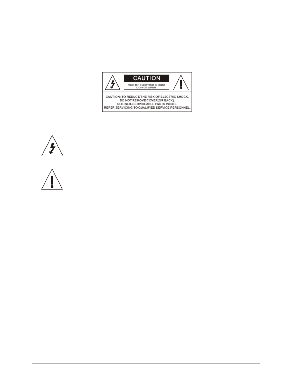
1. Warning
TO REDUCE THE RISK OF FIRE OR ELECTRIC SHOCK:
DO NOT EXPOSE THIS PRODUCT TO RAIN OR MOISTURE.
DO NOT INSERT ANY METALLIC OBJECT THROUGH VENTILATION GRILLS.
CAUTION:
Explanation of Graphical Symbols
The lightning flash with arrowhead symbol, within an equilateral triangle, is
intended to alert the user to the presence of non-insulated dangerous voltage
within the product's enclosure that may be of sufficient magnitude to
constitute a risk of electric shock to persons.
The exclamation point within an equilateral triangle is intended to alert the
user to the presence of important operating and maintenance (servicing)
instructions in the literature accompanying the product.
2. Precautions
2.1. Safety
Should any liquid or solid object fall into the cabinet, unplug the unit and have it checked by
the qualified personnel before operating it any further. Unplug the unit from the wall outlet
if it is not going to be used for several days or more. To disconnect the cord, pull it out by
the plug. Never pull the cord itself. Allow adequate air circulation to prevent internal heat
built-up. Do not place the unit on surfaces (rugs, blankets, etc.) or near materials (curtains,
draperies) that may block the ventilation holes.
2.2. Installation
Do not install the unit in an extremely hot or humid place or in a place subject to excessive
dust or mechanical vibration. The unit is not designed to be waterproof. Exposure to rain or
water may damage the unit.
2.3. Cleaning
Clean the unit with a slightly damp soft cloth. Use a mild household detergent. Never use
strong solvents such as thinner or benzine as they might damage the finish of the unit.
Retain the original carton and packing materials for safe transport of this unit in the future.
Doc # INS-45S17 Issue Date: 02/02/07
Revision: A Page 3 of 12
3. Federal Communications Commission (FCC) Statement
This Equipment has been tested and found to comply with the limits for a Class B digital
device, pursuant to Part 15 of the FCC rules. These limits are designed to provide
reasonable protection against harmful interference in a residential installation. This
equipment generates, uses and can radiate radio frequency energy and, if not installed and
used in accordance with the instructions, may cause harmful interference to radio
communications. However, there is no guarantee that interference will not occur in a
particular installation. If this equipment does cause harmful interference to radio or
television reception, which can be determined by turning the equipment off and on, the user
is encouraged to try to correct the interference by one or more of the following measures:
• Reorient or relocate the receiving antenna.
• Increase the separation between the equipment and receiver.
• Connect the equipment into an outlet on a circuit different from that to which the
receiver is connected.
• Consult the dealer or an experienced radio/TV technician for help.
You are cautioned that changes or modifications not expressly approved by that party
responsible for compliance could void your authority to operate the equipment.
This device complies with Part 15 FCC Rules. Operation is subject to the
following two conditions:
(1) This device may not cause harmful interference.
(2) This device must accept any interference received including interference
that may cause undesired performance.
Doc # 45M17 Issue Date: 11/09/05
Revision: B Page 4 of 12
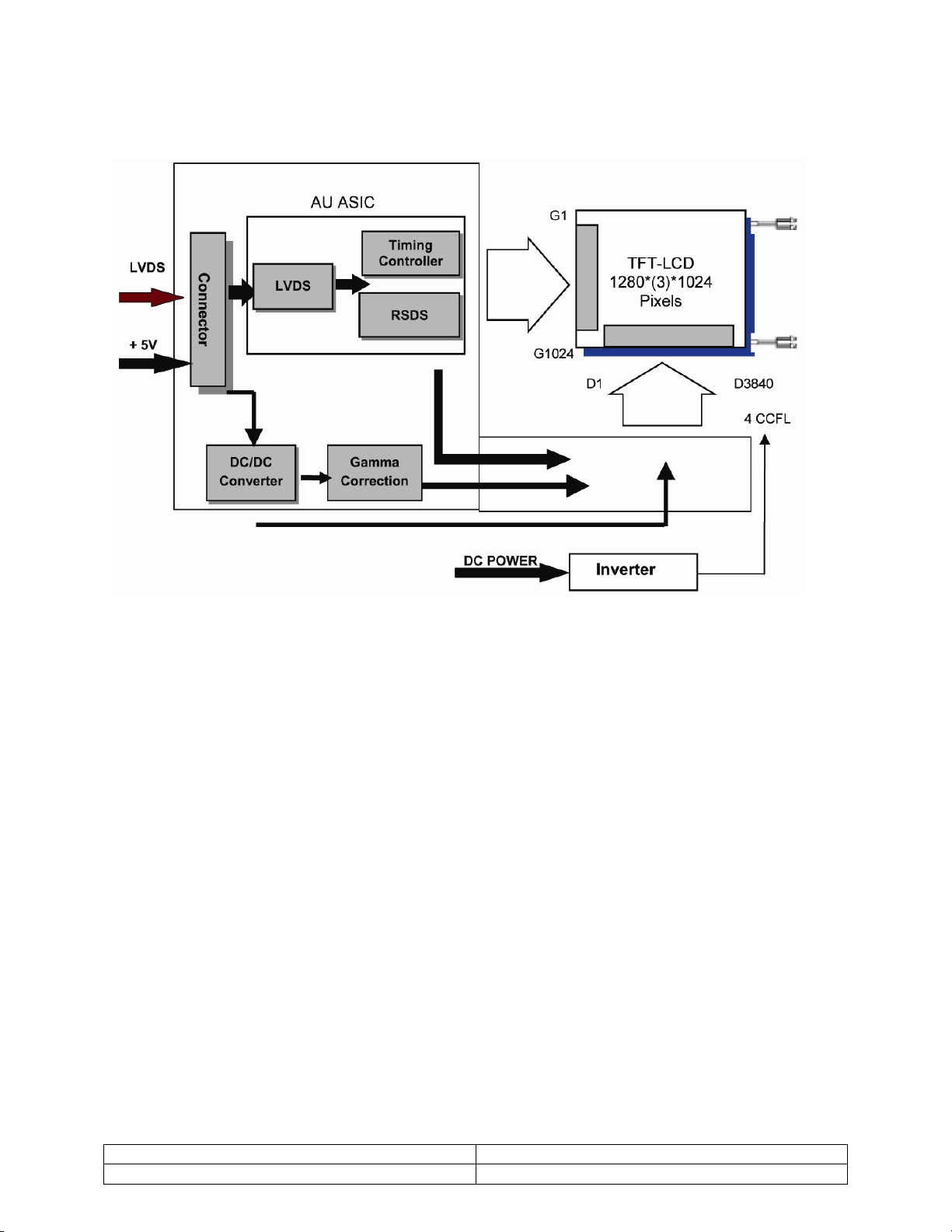
4. Functional Block Diagram
The following diagram shows the functional block of the 17.0 inches Color TFT / LCD
Module:
Doc # 45M17 Issue Date: 11/09/05
Revision: B Page 5 of 12
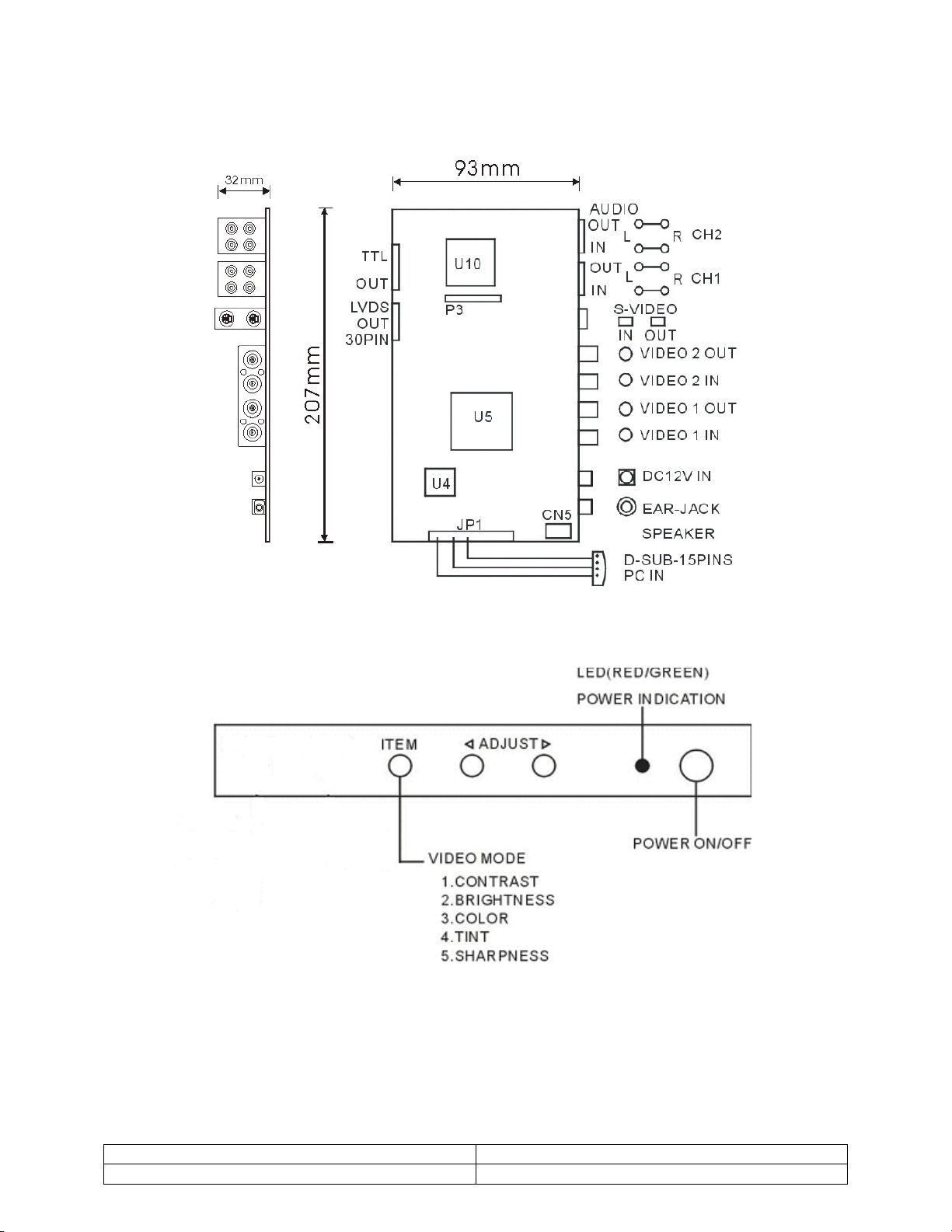
5. Module Connector P in Configuration
The module using a pair of LVDS receivers SN75LVDS82 (Texas Instruments) or compatible.
LVDS is a differential signal technology for LCD interface and high peed data transfer
device. Transmitter shall be SN75LVDS83 (negative edge sampling) or compatible. The first
LVDS port (RxOxxx) transmits odd pixels wile the second LVDS port (RxExxx) transmits
even pixels.
PIN# SIGNAL NAME DESCRIPTION
1 RxOIN0- Negative LVDS Differential Data Input (Odd Data)
2 RxOIN0+ Positive LVDS Differential Data Input (Odd Data)
3 RxOIN1- Negative LVDS Differential Data Input (Odd Data)
4 RxOIN1+ Positive LVDS Differential Data Input (Odd Data)
5 RxOIN2- Negative LVDS Differential Data Input (Odd Data, H-Sync, V-
Sync, DSPTMG)
6 RxOIN2+ Positive LVDS Differential Data Input (Odd Data, H-Sync, V-Sync,
DSPTMG)
7 VSS Power Ground
8 RxOCLKIN- Negative LVDS Differential Clock Input (Odd Data)
9 RxOCLKIN+ Positive LVDS Differential Clock Input (Odd Data)
10 RxOIN3- Negative LVDS Differential Data Input (Odd Data)
11 RxOIN+ Positive LVDS Differential Data Input (Odd Data)
12 RxEIN0- Negative LVDS Differential Data Input (Even Data)
13 RxEIN0+ Positive LVDS Differential Data Input (Even Data)
14 VSS Power Ground
15 RxEIN1- Negative LVDS Differential Data Input (Even Data)
16 RxEIN1+ Positive LVDS Differential Data Input (Even Data)
17 VSS Power Ground
18 RxEIN2- Negative LVDS Differential Data Input (Even Data)
19 RxEIN2+ Positive LVDS Differential Data Input (Even Data)
20 RxECLKIN- Negative LVDS Differential Clock Input (Even Data)
21 RxECLKIN+ Positive LVDS Differential Clock Input (Even Data)
22 RxEIN3- Negative LVDS Differential Data Input (Even Data)
23 RxEIN3+ Positive LVDS Differential Data Input (Even Data)
24 VSS Power Ground
25 VSS Power Ground
26 NC No Connection (for AUO test)
27 VSS Power Ground
28 VCC +5.0V Power Supply
29 VCC +5.0V Power Supply
30 VCC +5.0V Power Supply
Doc # 45M17 Issue Date: 11/09/05
Revision: B Page 6 of 12
6. Inspection Standard
6.1. Inspection environment conditions
Room Temperature: 20~25°
Humidity: 65±5% RH
6.2. The viewing line should be perpendicular to the surface screen.
Dot defect
a) Inspection condition
Inspection distance: 35±5cm
Inspection illumination: 100~150Lux
Panel temperature: 30±5
Inspection pattern: Full white, full black, red, green and blue screens.
b) Acceptable
Area
Item A B
Total
Blue Black 2 3 4
Red Green White 1 3 3
Total 2 5 7
c) The definitions of A and B zone
B
A
V/2 V/4
V
H/4 H/2
H
Scratch on the polarizer
Number = 3 max.
Width 0.1 mm, Length 6 mm
Dent on the polarizer
Number = 3 max, Average Diameter ∅0.3 mm
Foreign material on the polarizer
Number = 2 max, Average Diameter ∅0.5 mm
Afterimage
After displaying a pattern for 5 seconds then switch to a different pattern, the previous
pattern should disappear within 10 seconds.
Doc # 45M17 Issue Date: 11/09/05
Revision: B Page 7 of 12
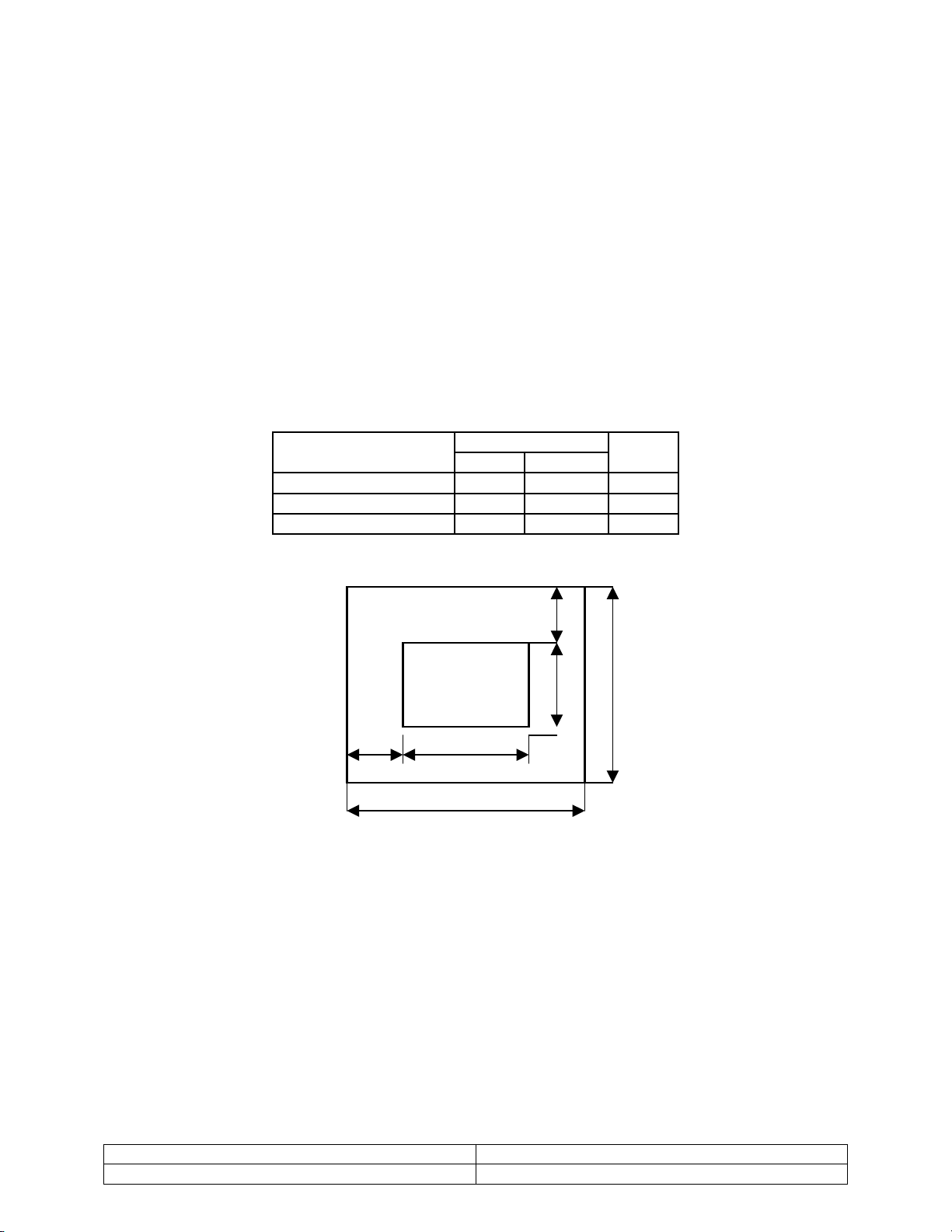
7. Specification
Electrical 45S17
Operating System NTSC / PAL / XGA / SXGA@60Hz / SVGA
Aspect Ratio 4:3
Picture Diagonal 17.25”
Active Area (W x H) 13.4” x 10.7” (337mm x 270mm)
Resolution (H x V) 1280 x 1024
Response Time 12ms
Video Angle Up / Down 800, Left / Right 800
Brightness 300 cd/m2
Contrast Ratio 500:1
Display Colors 16.2M
Video Input/Output Video: 1 CH Composite video 1Vp-p 75ohm
In/Out Impedance 75 ohms/ auto termination
Power Source 12V DC
Power Consumption 4.5A / 30W
Environmental
Ambient Operating
Temperature 0° C ~ 50° C (32°F ~ 122°F)
Operating Humidity 20% - 60% R. H.
Mechanical
Dimensions W x H x D 358mm x 296mm x 17mm (14.1” x 11.6” x 0.67”)
Weight 1.9g (0.004 lbs)
Connectors Video: 1CH BNC input/output
Safety Standards FCC, CE, UL
Optical
Lamp Life-time 30,000hr min.
Viewing Angle (Typ.) CR=5 Right, Left, Top, Down = 80 deg
Brightness 300 nit (typ.)
Contrast Ratio 500:1 typical
Response Time Tr: 6 ms Tƒ: 2ms (Typ)
Doc # 45M17 Issue Date: 11/09/05
Revision: B Page 8 of 12
8. The Reference of Input Application
8.1. Drive Board w/Input Connectors
8.2. Function Key Board
Doc # 45M17 Issue Date: 11/09/05
Revision: B Page 9 of 12
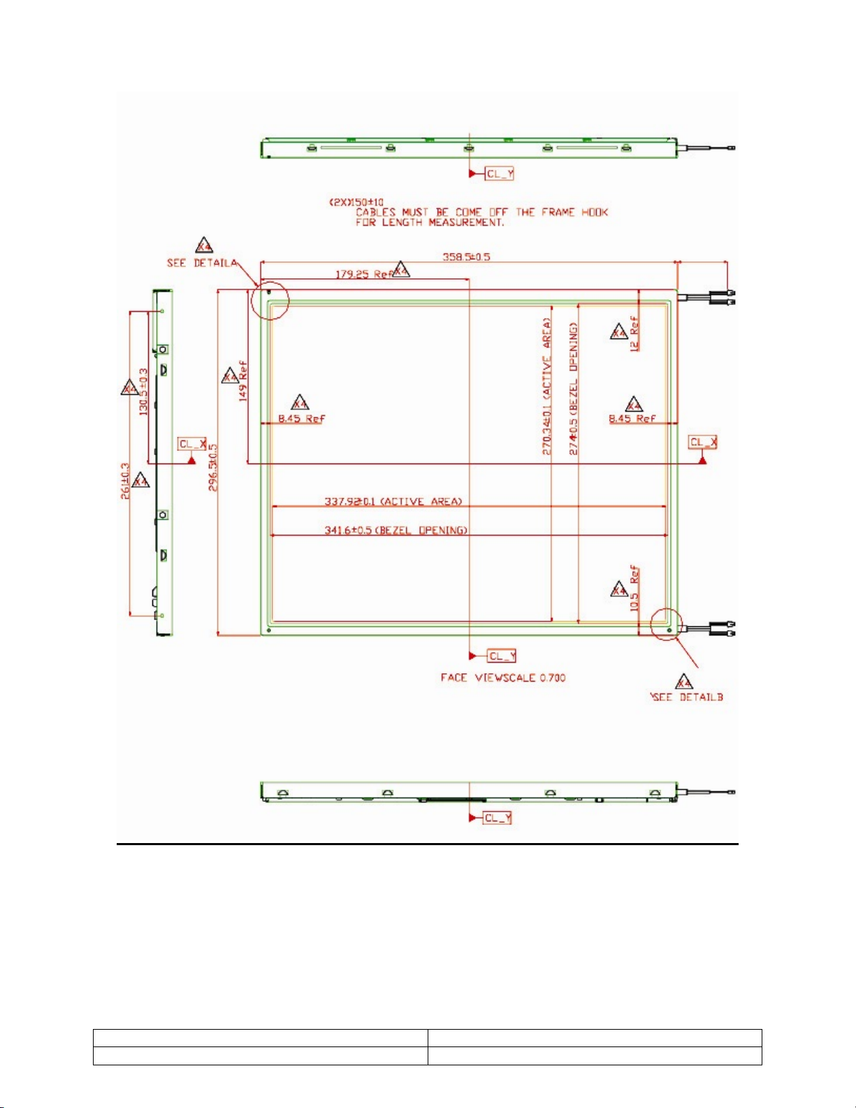
9. Mechanical Characteristics
Doc # 45M17 Issue Date: 11/09/05
Revision: B Page 10 of 12
Table of contents
Other Videology Control Unit manuals


Popular Control Unit manuals by other brands

Festo
Festo Compact Performance CP-FB6-E Brief description

Elo TouchSystems
Elo TouchSystems DMS-SA19P-EXTME Quick installation guide

JS Automation
JS Automation MPC3034A user manual

JAUDT
JAUDT SW GII 6406 Series Translation of the original operating instructions

Spektrum
Spektrum Air Module System manual

BOC Edwards
BOC Edwards Q Series instruction manual

KHADAS
KHADAS BT Magic quick start

Etherma
Etherma eNEXHO-IL Assembly and operating instructions

PMFoundations
PMFoundations Attenuverter Assembly guide

GEA
GEA VARIVENT Operating instruction

Walther Systemtechnik
Walther Systemtechnik VMS-05 Assembly instructions

Altronix
Altronix LINQ8PD Installation and programming manual


