Watec WAT-910BD Use and care manual

WAT-910BD SPI COMMUNICATION MANUAL(Digital Out)
WAT-910BD
SPI COMMUNICATION MANUAL(Digital Out)
Ver.1.0
Jul.01,2016
Watec Co.,Ltd.

WAT-910BD SPI COMMUNICATION MANUAL(Digital Out)
History
Ver. No.
Date
Changes
Remark
1.00
2016.07.01
First edition
- i -

WAT-910BD SPI COMMUNICATION MANUAL(Digital Out)
1. INTRODUCTION
2. LEGAL DISCLAIMER
3. OVERVIEW
4. SPI COMMUNICATION
5. DEGITAL OUTPUT FUNCTION SETTING
5.1 DIGITAL OUTPUT ON/OFF
5.2 DETAIL SETTINGS
5.2.1 CLOCK PHASE (CLK PHASE)
5.2.2 COLOR ID (COLOR ID)
5.2.3 OUTPUT DATA RANGE (DYC RANGE)
5.2.4 DIGITAL OUTPUT ON/OFF (DIGIT OUT)
5.3 DEGITAL OUTPUT GAIN (DIGITAL Y GAIN)
Contents
.................................... 1
.................................... 1
.................................... 1
.................................... 2
.................................... 4
.................................... 4
.................................... 8
- ii -
.................................... 5
.................................... 5
.................................... 6
.................................... 7
.................................... 8

WAT-910BD SPI COMMUNICATION MANUAL(Digital Out)
This manual is a supplement manual for using the digital output of the WAT-910BD.
Therefore, it is recommended that this manual is read in conjunction with the "WAT-910BD H / W manual".
Description requiring electrical knowledge needed to properly use the camera is included in the contents of this
document. Please read this document carefully, and use and/or install the camera after full understanding.
Under improper installation, it may cause serious damage to the connected equipment and the camera.
Please contact the distributor or dealer from which the WAT-910BD was purchased, if you do not understand the
installation, operation or safety instructions laid out in our manuals.
In addition, how to operate and install the camera, please refer "WAT-910BD Operation Manual" together with this
document.
Design and specifications are subject to change for improvement without notice.
Watec is not responsible for any inconvenience or damages to the video and monitoring recording equipment
caused by misuse, mis-operation or improper wiring of our equipment.
Technical information contained herein is for reference only and does not convey any license by any implication
or otherwise under any intellectual property right or other right of Watec or third parties.
Watec does not assume responsibility for any right infringements arising out of the use of this information.
This document describes how to set and to adjust the the digital output function by using the SPI communication
function of WAT-910BD.
Please refer to Chapter 6 of "WAT-910BD H / W manual" to know that how to use the SPI communication function.
About the video format of the digital output, please refer to Chapter 5 of "WAT-910BD H / W Manual".
2. LEGAL DISCLAIMER
1. INTRODUCTION
3. OVERVIEW
- 1 -

WAT-910BD SPI COMMUNICATION MANUAL(Digital Out)
In order to operate the related parameters of the digital output function, use the following commands.
1) CAMERA PARAMETER READ
SPI Write "data set" (send to camera MCU), Address:0x082
Checksum (CS) specifies the lower 1 byte of the calculated value (C1 + C2 + ADR + DAT).
In the PARAMETER READ command (address:0x082) , it will be 0x87 fixed value.
SPI Write "data set" (send to camera MCU), Address:0x193
Checksum (CS) specifies the lower 1 byte of the calculated value (C1 + C2 + ADR + DAT).
In the PARAMETER READ command (address:0x193) , it will be 0x99 fixed value.
SPI Read "data set" (camera MCU response)
*1: Parameter address lower byte. Same as SPI Write data.
*2: Paramwter value
*3: Check sum (lower byte of "ADR + DAT")
*4: ST CODE(AA:in execution 55:EXEC.NORMALLY A5:EXEC.ERROR)
Value
*1
*2
*3
*4
AA
Symbol
ADR
DAT
CS
ST
Value
04
02
93
00
99
AA
Symbol
C1
C2
ADR
DAT
CS
ST
Value
04
01
82
00
87
4.SPI COMMUNICATION
Symbol
C1
C2
ADR
DAT
CS
ST
- 2 -

WAT-910BD SPI COMMUNICATION MANUAL(Digital Out)
2) CAMERA PARAMETER WRITE
SPI Write "data set" (send to camera MCU), Address:0x082
*1: Parameter Value.
*2: Checksum (CS) specifies the lower 1 byte of the calculated value (C1 + C2 + ADR + DAT).
SPI Write "data set" (send to camera MCU), Address:0x193
*1: Parameter Value.
*2: Checksum (CS) specifies the lower 1 byte of the calculated value (C1 + C2 + ADR + DAT).
SPI Read "data set" (camera MCU response)
*1: Parameter address lower byte. Same as SPI Write data.
*2: Paramwter value
*3: Check sum (lower byte of "ADR + DAT")
*4: ST CODE(AA:in execution 55:EXEC.NORMALLY A5:EXEC.ERROR)
Symbol
ADR
DAT
CS
ST
Value
*1
*2
*3
*4
ST
Value
04
82
93
*1
*2
AA
Symbol
C1
C2
ADR
DAT
CS
CS
ST
Value
04
81
82
*1
*2
AA
Symbol
C1
C2
ADR
DAT
- 3 -

WAT-910BD SPI COMMUNICATION MANUAL(Digital Out)
Camera Parameter
*Factory setting value: 0x00
By using DIGIT OUT(0x5E2:Bit0), the digital output will be turned ON/OFF.
Since no other parameters are allocated in this address, digital output turning ON or OFF is possible by sending
data 0x01(ON) or 0x00(OFF).
e.g.1) turn ON the digital output function
Send following data bytes to the indirect registers for SPI control (address: 0x0036 to 0x003B).
e.g.2) turn OFF the digital output function
Send following data bytes to the indirect registers for SPI control (address: 0x0036 to 0x003B).
5. DEGITAL OUTPUT FUNCTION SETTING
5.1 DIGITAL OUTPUT ON/OFF
Address
Bit
7
6
5
4
3
2
1
0
-
-
-
-
DIGIT OUT
0:OFF
1:ON
address
0x36
0x37
0x38
0x39
0x3A
0x3B
0x5E2
-
-
-
symbol
C1
C2
ADR
DAT
CS
ST
value(hex)
00
81
E2
01
64
AA
address
0x36
0x37
0x38
0x39
0x3A
0x3B
symbol
C1
C2
ADR
DAT
CS
ST
value(hex)
00
81
E2
00
63
AA
- 4 -

WAT-910BD SPI COMMUNICATION MANUAL(Digital Out)
5.2.1 CLOCK PHASE (CLK PHASE)
By using the bit-3, the phase of digital output clock signal DCK (connector: J6, pin number: 4) is inverted.
Camera Parameter
*Factory setting value: 0x47
*1) CLK PHASE=0(factory setting):
In synchronization with the rising edge of the DCK, the digital video data is output.
DCK
*2)CLK PHASE=1:
In synchronization with the falling edge of the DCK, the digital video data is output.
DCK
e.g.3) To be synchronized with the falling edge of the data output by changing the DCK phase.
(digital output ON, others are left at the default setting)
The data byte to be transmitted to the digital output setting(address: 0x193) is 0xCF.
Send following data bytes to the indirect registers for SPI control (address: 0x0036 to 0x003B).
1
1
1:ON
1: 1-254
2:Cr,Y,Cb,Y
3:Y,Cr,Y,Cb
1:↓
Address
Bit
7
6
5
4
3
2
1
0
5.2 DETAIL SETTINGS
Bit
7
6
5
4
3
2
1
0
0x193
DIGIT OUT
DYC RANGE
COLOR ID
CLK PHASE
(fixed)
(fixed)
(fixed)
0:OFF
0:16-235
0:Cb,Y,Cr,Y
1:Y,Cb,Y,Cr
0:↑
1
Yn+4
Parameter
DIGIT OUT
DYC RANGE
COLOR ID
CLK PHASE
D7-D0 OUT
Yn
80
Yn+1
80
Yn+2
80
Yn+3
80
1:ON
1:1-254
0:Cb,Y,Cr,Y
1:↓
(fixed)
(fixed)
(fixed)
D7-D0 OUT
Yn
80
Yn+1
80
Yn+2
80
Yn+3
80
Yn+4
bit setting
1
1
0
0
1
1
1
1
data value
0xCF
address
0x36
0x37
0x38
0x39
0x3A
0x3B
symbol
C1
C2
ADR
DAT
CS
ST
value(hex)
04
82
93
CF
E8
AA
- 5 -

WAT-910BD SPI COMMUNICATION MANUAL(Digital Out)
5.2.2 COLOR ID (COLOR ID)
By using the bit-4 and 5, the data output order of the digital output signal bit 7 to 0
(connector: J6, pin number: 6-12) are changed.
Camera Parameter
*Factory setting value: 0x47
By using Bit-4, the output order of the chroma signal(Cb,Cr) and the luminance signal(Y) is changed.
By using Bit-5, the output order of the chroma signal(Cb) and the chroma signal(Cr) is changed.
(Since WAT-910BD is a B/W camera, bit-5 is invalid for substantially, and the data values of Cb and Cr are
all 0x80.)
The factory setting value is (bit-5, bit-4) = (0,0), it means that the digital data order are (Cb, Y, Cr, Y).
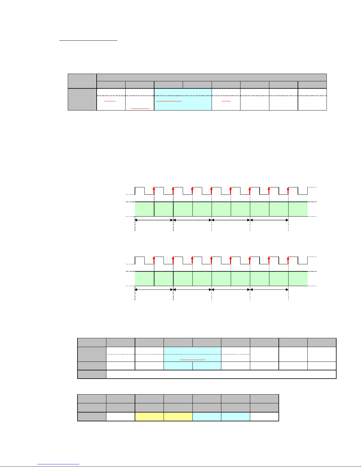
*1) COLOR ID=0 (factory setting) or 2:
The digital video data order are 0x80, Yn, 0x80, Yn+1…
DCK
*1) COLOR ID=1 or 3:
The digital video data order are Yn, 0x80, Yn+1, 0x80…
DCK
e.g.4) To change the order of the digital data to "luminance data first output".
(digital output ON, others are left at the default setting)
The data byte to be transmitted to the digital output setting(address: 0x193) is 0xD7.
Send following data bytes to the indirect registers for SPI control (address: 0x0036 to 0x003B).
7
6
5
4
3
2
1
0
0x193
DIGIT OUT
DYC RANGE
COLOR ID
CLK PHASE
(fixed)
(fixed)
(fixed)
0:OFF
0:16-235
0:Cb,Y,Cr,Y
1:Y,Cb,Y,Cr
0:↑
1
1
1
1:ON
1: 1-254
2:Cr,Y,Cb,Y
3:Y,Cr,Y,Cb
1:↓
Address
Bit
80
pixel data : n
pixel data : n+1
pixel data : n+2
pixel data : n+3
D7-D0 OUT
80
Yn
80
Yn+1
80
Yn+2
80
Yn+3
Yn+4
D7-D0 OUT
Yn
80
Yn+1
80
Yn+2
80
Yn+3
80
pixel data : n
pixel data : n+1
pixel data : n+2
pixel data : n+3
・・・
・・・
Bit
7
6
5
4
3
2
1
0
Parameter
DIGIT OUT
DYC RANGE
COLOR ID
CLK PHASE
(fixed)
(fixed)
(fixed)
1:ON
1:1-254
1:Y,Cb,Y,Cr
0:↑
bit setting
1
1
0
1
0
1
1
1
data value
0xD7
address
0x36
0x37
0x38
0x39
0x3A
0x3B
symbol
C1
C2
ADR
DAT
CS
ST
value(hex)
04
82
93
D7
F0
AA
- 6 -

WAT-910BD SPI COMMUNICATION MANUAL(Digital Out)
5.2.3 OUTPUT DATA RANGE (DYC RANGE)
By using the bit-6, the data output range of the digital output signal bit 7 to 0
(connector: J6, pin number: 6-12) are changed.
Camera Parameter
*Factory setting value: 0x47
16
e.g.5) To change the range of the digital output value to 16-235.
(digital output ON, others are left at the default setting)
The data byte to be transmitted to the digital output setting(address: 0x193) is 0x87.
Send following data bytes to the indirect registers for SPI control (address: 0x0036 to 0x003B).
symbol
C1
C2
ADR
DAT
CS
(fixed)
(fixed)
Bit
7
6
5
4
3
2
1
0
1
1
Parameter
DIGIT OUT
DYC RANGE
COLOR ID
CLK PHASE
1:ON
0:16-235
0:Cb,Y,Cr,Y
0:↑
(fixed)
ST
value(hex)
04
82
93
87
A0
AA
data value
0x87
address
0x36
0x37
0x38
0x39
0x3A
0x3B
bit setting
Address
Bit
7
6
5
4
3
2
1
0
(fixed)
0:OFF
0:16-235
0:Cb,Y,Cr,Y
1:Y,Cb,Y,Cr
0:↑
1
1
1
1:ON
1: 1-254
2:Cr,Y,Cb,Y
3:Y,Cr,Y,Cb
1:↓
DYC RANGE = 0
DYC RANGE = 1
0x193
DIGIT OUT
DYC RANGE
COLOR ID
CLK PHASE
(fixed)
(fixed)
dark
bright
254
235
1
output value(descimal)
brightness of the target
1
0
0
0
0
1
- 7 -

WAT-910BD SPI COMMUNICATION MANUAL(Digital Out)
5.2.4 DIGITAL OUTPUT ON/OFF (DIGIT OUT)
By using DIGIT OUT, the digital output will be turned ON/OFF.(It is same function as address 0x5E2 Bit-0.)
Camera Parameter
*Factory setting value: 0x47
e.g.6) turn ON the digital output function
(Others are left at the default setting)
The data byte to be transmitted to the digital output setting(address: 0x193) is 0xC7.
Send following data bytes to the indirect registers for SPI control (address: 0x0036 to 0x003B).
5.3 DEGITAL OUTPUT GAIN (DIGITAL Y GAIN)
By using this address byte, the gain of the digital data is adjustable.
Camera Parameter
*Factory setting value: 0xA0
e.g.7) To change the gain of digital data to 0xB0.
Send following data bytes to the indirect registers for SPI control (address: 0x0036 to 0x003B).
Address
Bit
7
6
5
4
3
2
1
0x082
DIGITAL Y GAIN
0x00 … 0xA0 … 0xFF
アドレス
0x36
0x37
0x38
0x39
0x3A
Address
Bit
7
6
5
4
3
2
AA
値
04
81
82
B0
B7
0x3B
シンボル
C1
C2
ADR
DAT
CS
ST
0
3:Y,Cr,Y,Cb
1:↓
Bit
5
4
1
0
0x193
DIGIT OUT
DYC RANGE
COLOR ID
CLK PHASE
(fixed)
(fixed)
(fixed)
0:OFF
0:16-235
0:Cb,Y,Cr,Y
1:Y,Cb,Y,Cr
0:↑
1
1
1
1:ON
1: 1-254
2:Cr,Y,Cb,Y
7
6
3
2
1
0
DIGIT OUT
DYC RANGE
COLOR ID
CLK PHASE
(fixed)
(fixed)
(fixed)
data value
0xC7
1:ON
1: 1-254
0:↑
Parameter
0:Cb,Y,Cr,Y
bit setting
1
1
0
0
0
1
1
1
値
04
82
93
C7
E0
AA
アドレス
0x36
0x37
0x38
0x39
0x3A
0x3B
シンボル
C1
C2
ADR
DAT
CS
ST
- 8 -
Other manuals for WAT-910BD
4
Table of contents
Other Watec Digital Camera manuals

Watec
Watec WAT-2200Mk-2 User manual

Watec
Watec WAT-232S User manual

Watec
Watec WAT-3200 User manual

Watec
Watec WAT-240E/FS User manual

Watec
Watec WAT-704R Series User manual

Watec
Watec WAT-240E User manual

Watec
Watec WAT- 1903XH3/RC User manual

Watec
Watec WAT-910BD User manual

Watec
Watec WAT-910HX Installation manual

Watec
Watec WAT-910HX3/RC User manual