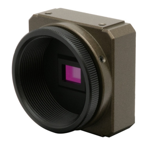
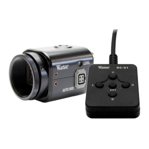
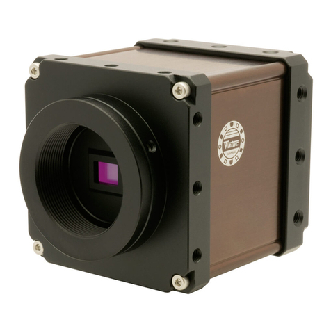
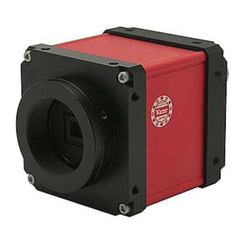
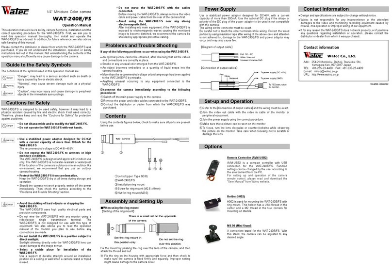
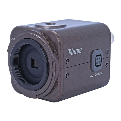
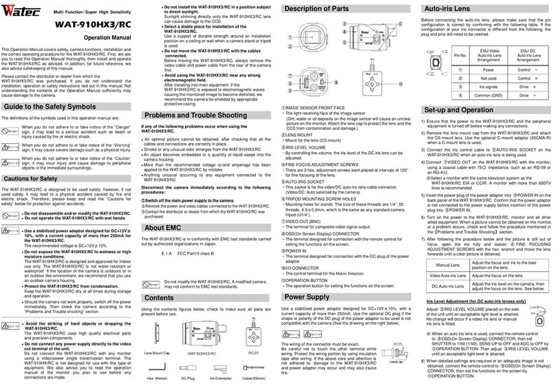
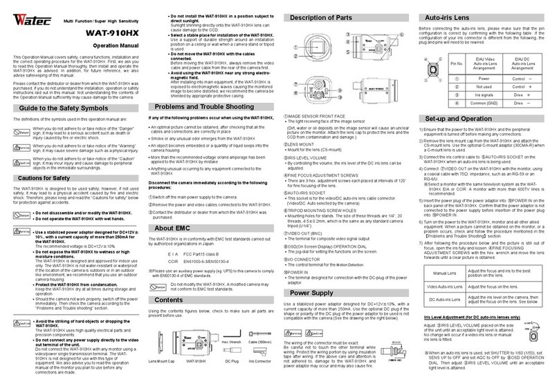
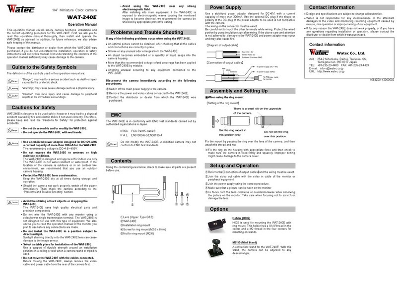
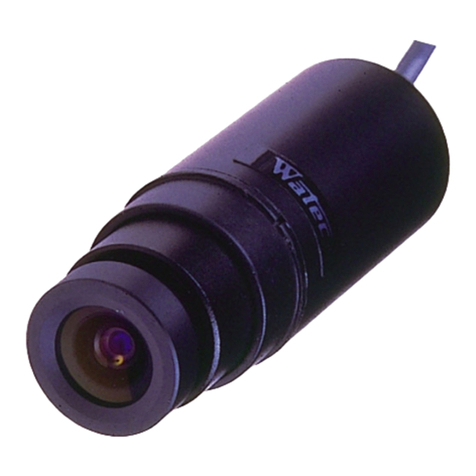
Watec WAT-910BD User manual

WAT-910BD H/W MANUAL
Ver.1.10
Jul. 01, 2016
WAT-910BD
Watec Co.,Ltd.
H/W MANUAL

WAT-910BD H/W MANUAL
History
1.10
2016.07.01
format(EIA and CCIR)
*P.23 resistor value change from 220k[ohm] to
4.7k[ohm]. Same change is in Fig.6-3.
Ver. No.
Date
Changes
Remark
First edition
correct: P.34 MANUAL GAIN bit range
correct: P.34 HSBLC WINDOW H/V SIZE address
correct: P.41 BPC LEVEL bit range
*Fix fine typos.
1.01
2013.12.25
1.00
2013.11.06
1.02
2014.10.23
- i -
*The page configuration of the English manual was
fit to the Japanese manual.
*The factory default values were appended to
"6.4 CAMERA PARAMETER".
*P.16-19 add H/V blanking timing to line data

WAT-910BD H/W MANUAL
1. INTRODUCTION
2. LEGAL DISCLAIMER
3. OVERVIEW
4. DESCRIPTION OF PARTS
4.1 POWER INPUT
4.2 VIDEO OUTPUT
4.3 DC IRIS LENS CONTROL
4.4 VIDEO IRIS LENS CONTROL
4.5 GPIO(MOTION DETECT)
4.6 OSD CONTROL
5. DIGITAL VIDEO OUT
5.1 ELECTRICAL CHARACTERISTICS
5.2 DIGITAL OUTPUT FORMAT
6. SPI COMMUNICATION
6.1 ELECTRICAL CHARACTERISTICS
6.2 CTL-COMMAND PROTOCOL
6.3 CAMERA CTL-COMMAND
6.4 CAMERA PARAMETER
6.5 SAMPLE CODE
7. SPECIFICATIONS
8. DIMENSIONS
Contents
.................................... 5
.................................... 12
.................................... 14
.................................... 6
.................................... 7
.................................... 1
.................................... 1
.................................... 1
.................................... 2
.................................... 22
.................................... 23
.................................... 8
.................................... 9
.................................... 10
.................................... 11
- ii -
.................................... 61
.................................... 62
.................................... 28
.................................... 31
.................................... 35
.................................... 50

WAT-910BD H/W MANUAL
This manual is to explain the hardware features of the WAT-910BD.
Description requiring electrical knowledge needed to properly use the camera is included in the contents of this
document.
Please read this document carefully, and use and/or install the camera after full understanding.
Under improper installation, it may cause serious damage to the connected equipment and the camera.
Please contact the distributor or dealer from which the WAT-910BD was purchased, if you do not understand the
installation, operation or safety instructions laid out in our manuals.
How to use the OSD(On-Screen Display) menu and setting each function, for more information, please refer to
"WAT-910BD OSD Manual" together. In addition, how to operate and install the camera, please refer
"WAT-910BD Operation Manual" together with this document.
Design and specifications are subject to change for improvement without notice.
Watec is not responsible for any inconvenience or damages to the video and monitoring recording
equipment caused by misuse, mis-operation or improper wiring of our equipment.
Technical information contained herein is for reference only and does not convey any license by any implication
or otherwise under any intellectual property right or other right of Watec or third parties.
Watec does not assume responsibility for any right infringements arising out of the use of this information.
WAT-910BD is an ultra-high sensitivity B/W board camera equipped with 1/2 " format CCD.
By adopting the latest high-sensitivity CCD and DSP with a variety of functions to the signal processing unit,
WAT-910BD realized various functions and higher performances.
* In addition to the automatic exposure control function, high speed shutter and the electronic iris,
WAT-910BD is equipped with low-speed shutter (multi-field integration) function for dark
field imaging. High-quality imaging is now possible by the combination of these functions without
the illumination of the object.
* By adopting the latest DSP to the video processing block, a variety of digital signal processing functions
such as noise reduction, dynamic range correction, white blemish correction and motion detection are
available.
* For setting each functions, you can use user-friendly OSD menu or SPI communication to directly set
the functions.
* Digital output (parallel output) terminal is equipped for the video output, in addition to the conventional
analog output
* Since WAT-910BD is small in size (42mm square) and lightweight (approx.40g)design, making it ideal for
building into a variety of applications.
1. INTRODUCTION
2. LEGAL DISCLAIMER
3. OVERVIEW
- 1 -

WAT-910BD H/W MANUAL
The name and function of each parts are as follows.
When wiring, please be careful of the following pin arrangement and connect correctly.
Name
Parts shape
(Fig.4-2) DC IRIS LENS adjustment VR
Description
4. DESCRIPTION OF PARTS
(Fig.4-1) Location of functional connectors
VR1
Adjustment VR
for DC IRIS Lens
clockwise : DC iris Lens toward to open
counterclockwise : DC iris Lens toward to close
*This adjustment is working only J3 output
close
J3
J4
J1
J7
J8
J5
J6
J2
VR1
open
- 2 -

WAT-910BD H/W MANUAL
(Fig.4-3) Connector Pin Function
JST
JST
JST
I/O
SPI SLD (active L)
⑭
①
SPI SDA
④
GND (common)
GND (common)
O
O
GND
③
GND
I
I
GND (common)
GND
O
O
GND(COMMON)
-
O
O
GND
O
O
O
O
O
O
O
GND
-
O
-
O
GND
O
GND
⑪
DATA 2
J7
SPI
Communication
BM04B-SRSS
⑫
DATA 1
⑬
DATA 0(LSB)
⑥
DATA 7(MSB)
⑦
DATA 6
②
SPI SCL
⑨
DATA 4
⑩
DATA 3
③
GND (common)
④
CLOCK
⑤
GND (common)
①
Vertical Blanking
②
Horizontal Blanking
J6
Digital Video
Output
BM14B-SRSS
⑧
DATA 5
③
(reserved)
J5
GPIO
JST
①
MOTION DETECT output
②
BM03B-SRSS
J3
NC(Non Conection)
④
Drive-
①
Vcc(DC+12V) OUT
molex
molex
J4
VIDEO IRIS
CTL.
53047-0410
②
④
DC IRIS CTL.
③
BM02B-SRSS
53047-0410
③
IRIS OUT
①
JST
VIDEO GND(COMMON)
Sense-
②
Sense+
Drive+
②
power GND(COMMON)
O
GND
J2
VIDEO OUT
①
VIDEO OUTPUT
②
Parts No.
manufacturer
I
GND
J1
POWER
BM02B-SRSS
①
power in(DC+12V)
I/O
Description
Parts Shape
Name
Pin No.
①
①
①
①
①
①
①
- 3 -

WAT-910BD H/W MANUAL
(Fig.4-3) Connector Pin Function (continued)
Parts Shape
Name
Parts No.
Pin No.
manufacturer
GND
I/O
Description
I
I
I
I
I
UP
DOWN
BM06B-GHS-TBT
①
GND(COMMON)
②
RIGHT
LEFT
JST
SET
J8
OSD CTL.
(5key
interface)
④
⑥
③
⑤
①
- 4 -

WAT-910BD H/W MANUAL
4.1 POWER INPUT
(1) Input Voltage
Recommended supply voltage range and the absolute maximum ratings
are as follows.
Normally, We recommend to use WAT-910BD in "Supply Voltage Range(recommended) ".
Using in range of "Supply Voltage Range(Capable)", the camera may be NOT damaged.
In this case(especially lower voltage condition), please check followings.
*When shooting a significantly brighter object, blooming or smear increases might occur.
*When using VIDEO IRIS LENS, the lens iris does not open, or the iris opening and closing is slow.
In the case of using "supply voltage range(capable)", please adopt it after fully evaluation of proper
operation of the camera/system.
In case of using power supply voltage exceed the maximum rating, it will cause a serious damage to camera
and/or to other equipment connecting to the camera.
(2) Power Consumption
Power consumption by the camera is about 1.32W. (Supply voltage: DC +12V, current consumption: 110mA)
This value is Typical. (It has been measured under the following conditions)
*Measuring condition:
1) The camera function settings are all default.(equal values after running the OSD menu "RESET")
2) Using a manual iris lens, the lens iris is fully closed.
The power consumption of the camera and efficiency depend on the supply voltage.
Under the above conditions, the measurement values of the power consumption and current consumption
related to the supply voltage are shown in following table.
Please note the following points in the selection and design of the power supply used.
* When a auto iris lens (Video iris/ DC iris) is used, the power consumption will increase.
The increment of current consumption is related to lens specification.
* By the combination of the camera functions to be used, the current value will change.
Please select or design power supply of enough performance, in consideration of camera usage.
12[V]+/-10[%]
Current Consumption(mA)
1.31
13.0
13.5
14.0
Supply Voltage Range (Reccommended)
item
Supply Voltage Range (Capable)
Absolute Maximum Ratings
10.5
12.5
DC +8.0 - 14.0[V]
less than DC +16.0[V]
value(range)
114.8
11.0
(Fig.4-4) Power input specifications
8.0
8.5
9.0
9.5
10.0
1.26
1.28
11.5
12.0
148.8
141.6
134.9
128.6
123.8
119.0
101.1
98.4
111.0
107.0
1.19
1.20
1.21
1.22
1.24
1.25
1.28
Supply Voltage(V)
Power Consumption(W)
95.7
*Note:
1.33
Power Consumption(W)
104.2
1.34
Typical value, Not guaranteed.
1.30
(Fig.4-5) Power Consumption(Typical)
Supply Voltage(V)
Current Consumption(mA)
J1: POWER INPUT
- 5 -

WAT-910BD H/W MANUAL
4.2 VIDEO OUTPUT
An analog video output terminal of 75 ohm impedance.
75 ohm termination is needed in the video signal receiver equipment.
Description
VIDEO GND(COMMON)
(Fig.4-6) VIDEO output
Parts Shape(Pin No.)
Pin Name
①
VIDEO OUTPUT
②
J2
75 ohm impedance
J2: VIDEO OUTPUT
①
- 6 -

WAT-910BD H/W MANUAL
4.3 DC IRIS LENS CONTROL
This connector is used to connect a DC IRIS LENS.
When connecting the lens, be careful to wire after
confirming the pin assignments.
(1) Wiring to the lens
Pin assignments of JEITA standard iris connector
and J3 connector terminal have one-to-one
correspondence as following.
(2) Adjustment method of the lens iris
The lens iris is adjusted with next steps.
STEP1: Fix the shutter speed by using OSD menu.(SETUP->EXPOSURE->SHUTTER)
Recommended setting of SHUTTER is either OFF(EIA:1/60,CCIR:1/50) or FL(EIA:1/100,CCIR:1/120).
STEP2: Turn off "SENSE UP" function.
STEP3: Turn off "AGC" function.
Set "GAIN" to the minimum value (6dB) by using "MANUAL GAIN" menu.
STEP4: Return to the EXPOSURE menu, by adjusting the VR1, set the proper lens iris.
STEP5: If the adjustment of lens iris is correct, when AGC is switched to LOW from OFF, the video signal
will be a little brighter.
STEP5: When switching to AGC LOW from OFF, and the video screen is to be slightly
STEP1,2: OSD SETTINGS
*4
*3
*4
brighter, it is the proper result of lens iris adjustment.
(Fig.4-5) Pin assignments of DC IRIS connector
Sense+
STEP3: MANUAL GAIN SETTING
STEP4: IRIS ADJUSTMENT
Drive-
*1
*2
*3
J3
*2
Sense-
female IRIS connector(JEITA spec.)
*1
Pin Name
②
Parts Shape(Pin No.)
③
④
Drive+
①
J3: IRIS Connector(for DC IRIS LENS)
VR1: Adjustment VR(for DC IRIS LENS)
①② ③ ④
open
close
- 7 -

WAT-910BD H/W MANUAL
4.4 VIDEO IRIS LENS CONTROL
This connector is used to connect a VIDEO IRIS LENS.
When connecting the lens, be careful to wire after confirming the pin
assignments.
(1) Wiring to the lens
Pin assignments of JEITA recommended iris connector and J4 connector
terminal have one-to-one correspondence as following.
(2) Adjustment method of the lens iris
How to adjust the lens iris is the same as the DC-iris lens, but location and function of the adjustment
VR is different by each lens used.
About the adjustment VR(location and function), please refer to the instruction manual of the lens.
④
*3
(Fig.4-6) Pin configuration of VIDEO IRIS connector
③
*3
*4
IRIS OUT
GND(COMMON)
*1
J4
*2
*4
Pin Name
Vcc(DC+12V) OUT
①
②
*2
NC(Non Conection)
female IRIS connector(JEITA spec.)
*1
Parts Shape(Pin No.)
J4: IRIS Connector(VIDEO DC IRIS LENS)
① ② ③ ④
- 8 -

WAT-910BD H/W MANUAL
4.5 GPIO(MOTION DETECT)
When using MOTION DETECTION function of WAT-910BD,
it is possible to output the detection results from GPIO connector.
For information about how to set up and use the motion detection feature,
please refer to the OSD manual.
Pin Name
OSD SETTING
Motion detecting message
(Fig.4-7) Pin configuration of GPIO(MOTION DETECT) connector
Output High Voltage
Voh
2.4
③
Parameter
Symbol
Remarks
Typ
Max
Parts Shape(Pin No.)
②
Description
Output Time
T
2
S
J5
(reserved)
Ioh = 1mA
(Fig.4-8) Electrical Characteristic Table (MOTION DETECT output)
V
①
MOTION DETECT output
voltage is changed to H level.
When detecting a motion, output
GND (common)
CAMERA GND(common)
Vol
0.4
V
Iol = -1mA
Unit
Output Low Voltage
Min
J5: GPIO
①
- 9 -

WAT-910BD H/W MANUAL
4.6 OSD CONTROL
In order to operate the OSD, either a remote controller (RC-01) or electrical
contacts(circuit) is required.
The terminals of the J8 are pulled up with resistors inside of the camera.
To move cursor and/or select a item on OSD, input the L pulse in each
terminals by touching with the GND terminal.
Latch
②
SET
Pin Name
Parts Shape(Pin No.)
GND(COMMON)
①
Repeat
J8
③
④
RIGHT
⑥
⑤
DOWN
UP
Repeat input:
While each pin is held in the L state, DSP
will repeat the latch operation.
Description
LEFT
L active
(Fig.4-9) Connector Pin Function
J8: OSD CTL.(5key interface)
①
- 10 -

WAT-910BD H/W MANUAL
Digital Video data can be output via the Digital Video Output Connector (J6) on the WAT-910BD.
Use the OSD Menu or the SPI communication to switch the Digital Video Data Output ON/OFF.
(1) Operation by OSD
From the [SETUP] menu, select [FUNCTIONS], from the [FUNCTIONS] menu, switch the [DIGITAL OUT] feature
between ON/OFF.
For details regarding the operation of the OSD menu, please refer to the OSD Manual.
(2) Operation through SPI Communication
By using the SPI communication, it is possible to switch the Digital Video Output ON/OFF without going through
the OSD menu.
Please refer to section 6. SPI Communication on how to communicate via SPI and details on the parameter
addresses.
(3)Digital Video Output Connector
The figure below shows the location of the Digital Video Output Connector (J6).
(Fig.5-2) Digital Output Connector(J6)
5. DIGITAL VIDEO OUT
PARAMETER NAME
ADDRESS
DESCRIPTION
DIGIT OUT
Ox5E2, bit 0
(Digital Output On/Off) 0:OFF, 1:ON
(Fig.5-1) SPI communication address (Digital out)
→
J6
- 11 -

WAT-910BD H/W MANUAL
Each pin of the J6 Connector is connected directly to the Camera's DSP through a resistor.
(3.3[V] CMOS level output. Does not go through buffer/driver.)
The pinouts for each pin and a simplified circuit diagram are shown below.
Parts No.
J6
①
③
Digital
Video
Output
④
Digital Clock(DCK)
(Fig.5-3) Pin Function Descreptions
-
O
Vertical Blanking
②
Horizontal Blanking
description
Parts shape
⑤
GND (common)
⑥
DATA 7(MSB)
⑦
DATA 6
⑨
DATA 4
⑩
DATA 3
⑧
DATA 5
5.1 ELECTRICAL CHARACTERISTICS
(Fig.5-4) partial schematic of Digital Video Output
O
O
O
O
O
O
Function
O
⑪
I/O
manufacturer
JST
O
O
Pin No.
-
O
⑬
DATA 0(LSB)
⑭
GND (common)
BM14B-SRSS
GND (common)
DATA 2
⑫
DATA 1
-
①
- 12 -

WAT-910BD H/W MANUAL
The electrical characteristics for each pin are as described below.
(Fig.5-5) Waveform and Sybols (DCK, DATA)
Output Low Voltage
Vol
(Fig.5-6) Electrical Characteristic Table (DCK, DATA)
Parameter
Symbol
Output High Voltage
Min
Typ
Voh
2.4
Tdl
Max
0.4
V
Iol = -6mA
Ioh = 6mA
V
Remarks
Unit
Tclk
34.9
DCK Cycle Time(EIA)
nS
1/(28.636363MHz)
34.9
Data Output Time(EIA)
Tdt
Data Output Delay Time
DCK Cycle Time(CCIR)
Tclk
35.2
1/(28.375MHz)
35.2
nS
nS
Data Output Time(CCIR)
Tdt
1.5
nS
nS
- 13 -

WAT-910BD H/W MANUAL
(1)Video Data Format
The WAT-910BD is a camera that conforms to the EIA/CCIR video format.
The Analog Video Output (Video Output Connector:J2) is a composite video output which conforms to the
EIA/CCIR standard, however, the digital video output does not fully comply with these standards.
The video format of the digital data output is in accordance with table 5.1-7.
(2)Data Format
The output digital data conforms to the ITU-R BT.656, however, the output data clock rate (DCK)
frequency is as shown in the figure below.
※Caution: Does not comply with the ITU-R BT.656 Standard DCK=27[MHz] output.
The Chroma Signal, Luminance Signal, Blanking Data, and TRC Data are output in sequence from the
Digital Output Connector (J6).
TRC Code, Chroma Signal, and Luminance Signal data format comply with the ITU-R BT.656 standards,
however, due to the difference in DCK frequency, the Blanking Data Number, Effective Data Number,
and Total Data Number do not comply with ITU-R BT.656(DCK=27MHz). The Figure below shows the output
data number for each.
EAV [Byte]
1440/1440
CCIR
28.375000
EIA
1716/1728
4
1512
1478
Effective DATA [Byte]
Total Data [Byte]
(Fig.5-9) Digital Data Format (1 Line Period)
EIA
CCIR
28.636363
SAV [Byte]
4/4
BLK(H) [Byte]
268/280
for reference
330
4/4
EIA
CCIR
ODD field
EVEN field
ODD field
EVEN field
27
(Fig.5-8) Digital Output Clock
241
1820
8
4
300
756
739
(BT.656 EIA/CCIR)
Active Video
[Line/Field]
[Line/Frame]
Blanking [Line/Field]
Effective Pixel [Pixel/line]
482
DCK [MHz]
Video Data level [Decimal]
1 - 254
5.1 DIGITAL OUTPUT FORMAT
Effective Data Bit [bit]
525
Frame rate [Frame/sec]
Total line [Line/Frame]
30
241
22
21
(Fig5-7) Digital Video Format
26
625
572
286
286
25
1808
- 14 -

WAT-910BD H/W MANUAL
(3)Output Timing for Digital Data
The effective image data is outputs the Luminance Data and Color Difference Data in Y/Cb/Cr=4:2:2 format.
(The output sequence is repeated in the Cb,Y,Cr,Y,… sequence)
Since the WAT-910BD is a monochrome camera, the Cb,Cr data are all 80[h].
The Horizontal Blanking Period (without TRC Code) is Cb,Cr=80[h], Y=10[h], repeated output.
The TRC Code, which is used to set the Efective Pixel Period, is output with every horizontal line.
The TRC Code complies with the ITU-R BT.656 standard, and output the 4 Byte Codes below.
SAV: Start of Active Video [hex]
EAV: End of Active Video [hex]
The 4th Byte of the TRC code (XX) is output according to the Figure below.
*NOTE: F=0 : during field 1 F=1 : during field 2
V=0 : elsewhere V=1 : during field blanking
H=0 : in SAV H=1 : in EAV
P0-P3 : protection bits
Fig.5-11(EIA)/Fig.5-12(CCIR) shows the output timing for 1 line worth of digital data.
Fig.5-13(EIA)/Fig.5-14(CCIR) shows the output timing for 1 frame worth of digital data.
F1
0
1
0
0
0
1
0
1
1
1
1
1
1
1
1
1
0
0
1
1
0
EC
1
1
1
1
0
C7
1
0
1
0
1
DA
9D
0
1
0
1
1
1
0
0
0
1
0
0
1
1
1
B6
0
1
0
1
1
1
0
1
AB
P3
P2
0
0
0
0
0
0
80
00
XX
CODE
[hex]
P1
P0
H
F
V
EVEN Field H Blanking(EAV)
bit0
bit7
bit6
bit5
bit4
bit3
ODD Field V Blanking(SAV)
EVEN Field V Blanking(SAV)
EVEN Field V Blanking(EAV)
ODD Field H Blanking(SAV)
ODD Field H Blanking(EAV)
ODD Field V Blanking(EAV)
EVEN Field H Blanking(SAV)
1
(Fig.5-10) TRC(Timing Reference Code)
1
(Fix)
1
0
bit2
bit1
FF
00
00
XX
FF
00
- 15 -

WAT-910BD H/W MANUAL
(1) EIA ODD Field(FLD1) V Blanking Timing
H Blanking
V Blanking
D7-D0 OUT
(Line #)
① EIA EVEN Field(FLD2) Active Video line
DCK
H Blanking
V Blanking
② EIA ODD Field(FLD1) Blanking line
DCK
H Blanking
V Blanking
80
10
FF
0
EAV code
H BLK DATA(Cb,Cr:80[h],Y:10[h]) 300[byte]
SAV code
V Blanking DATA (Cb,Cr:80[h],Y:10[h]) 1512[byte]
80
10
10
10
80
10
80
10
80
10
80
80
10
80
80
10
FF
0
0
AB
80
10
80
10
80
10
80
10
FF
0
0
B6
7[DCK]
30
31
32
Active Video Data (Cb,Cr:80[h], Y1-Y756:luminance DATA(01-FE)[h] ) 1512[byte]
1820[DCK/Line]
8[DCK]
7[DCK]
Y755
80
Y752
80
Y753
80
Y754
80
Y756
FF
0
EAV code
SAV code
Y755
Y753
80
Y754
80
H BLK DATA(Cb,Cr:80[h],Y:10[h]) 300[byte]
7[DCK]
4[DCK]
300[DCK]
4[DCK]
1512[DCK]
Y3
80
Y752
80
D7-D0 OUT
10
80
10
80
C7
80
Y1
80
Y2
80
10
80
10
FF
0
0
DA
80
10
80
10
80
4[DCK]
300[DCK]
4[DCK]
1512[DCK]
D7-D0 OUT
80
Y756
FF
0
0
22[Line]
FLD2(EVEN FLD)
FLD1(ODD FLD)
①
②
1820[DCK/Line]
524
525
1
2
8[DCK]
7[DCK]
(Fig 5-11a) Line Data Format (EIA)
10
80
10
515
516
517
518
519
520
521
522
523
3
4
5
6
7
8
19
20
9
10
11
12
13
14
34
25
26
27
28
15
16
17
18
29
33
21
22
23
24
- 16 -

WAT-910BD H/W MANUAL
(2) EIA EVEN Field(FLD2) V Blanking Timing
H Blanking
V Blanking
D7-D0 OUT
(Line #)
③ EIA ODD Field(FLD1) Active Video line
DCK
H Blanking
V Blanking
④ EIA EVEN Field(FLD2) Blanking line
DCK
H Blanking
V Blanking
10
FF
0
EAV code
H BLK DATA(Cb,Cr:80[h],Y:10[h]) 300[byte]
SAV code
V Blanking DATA (Cb,Cr:80[h],Y:10[h]) 1512[byte]
10
80
10
80
10
80
80
10
80
10
80
0
EC
80
10
80
10
80
10
80
10
FF
0
0
F1
80
10
80
10
80
10
80
10
FF
0
D7-D0 OUT
10
80
10
80
10
1820[DCK/Line]
7[DCK]
4[DCK]
300[DCK]
4[DCK]
1512[DCK]
80
Y756
FF
0
EAV code
H BLK DATA(Cb,Cr:80[h],Y:10[h]) 300[byte]
SAV code
Active Video Data (Cb,Cr:80[h], Y1-Y756:luminance DATA(01-FE)[h] ) 1512[byte]
80
Y753
80
Y754
80
Y755
Y2
80
Y3
80
Y752
0
0
80
80
Y1
80
10
80
10
80
10
FF
0
0
9D
80
10
80
Y754
80
Y755
80
Y756
FF
7[DCK]
4[DCK]
300[DCK]
4[DCK]
1512[DCK]
D7-D0 OUT
Y752
80
Y753
80
297
FLD1(ODD FLD)
FLD2(EVEN FLD)
③
④
1820[DCK/Line]
291
292
293
294
295
296
285
286
287
288
289
290
279
280
281
282
283
284
273
274
275
276
277
278
267
268
269
270
271
272
261
262
263
264
265
266
22[Line]
253
254
255
256
257
258
259
260
8[DCK]
8[DCK]
7[DCK]
7[DCK]
(Fig 5-11b) Line Data Format (EIA)
- 17 -
Other manuals for WAT-910BD
4
Table of contents
Other Watec Digital Camera manuals

Watec
Watec WAT-240E User manual

Watec
Watec WAT-910BD Use and care manual

Watec
Watec WAT-240E/FS User manual

Watec
Watec WAT-910HX3/RC User manual

Watec
Watec WAT-704R Series User manual

Watec
Watec WAT-2500 User manual

Watec
Watec WAT-910HX Installation manual

Watec
Watec WAT-233 User manual

Watec
Watec WAT-2200 User manual

Watec
Watec WAT-232S User manual