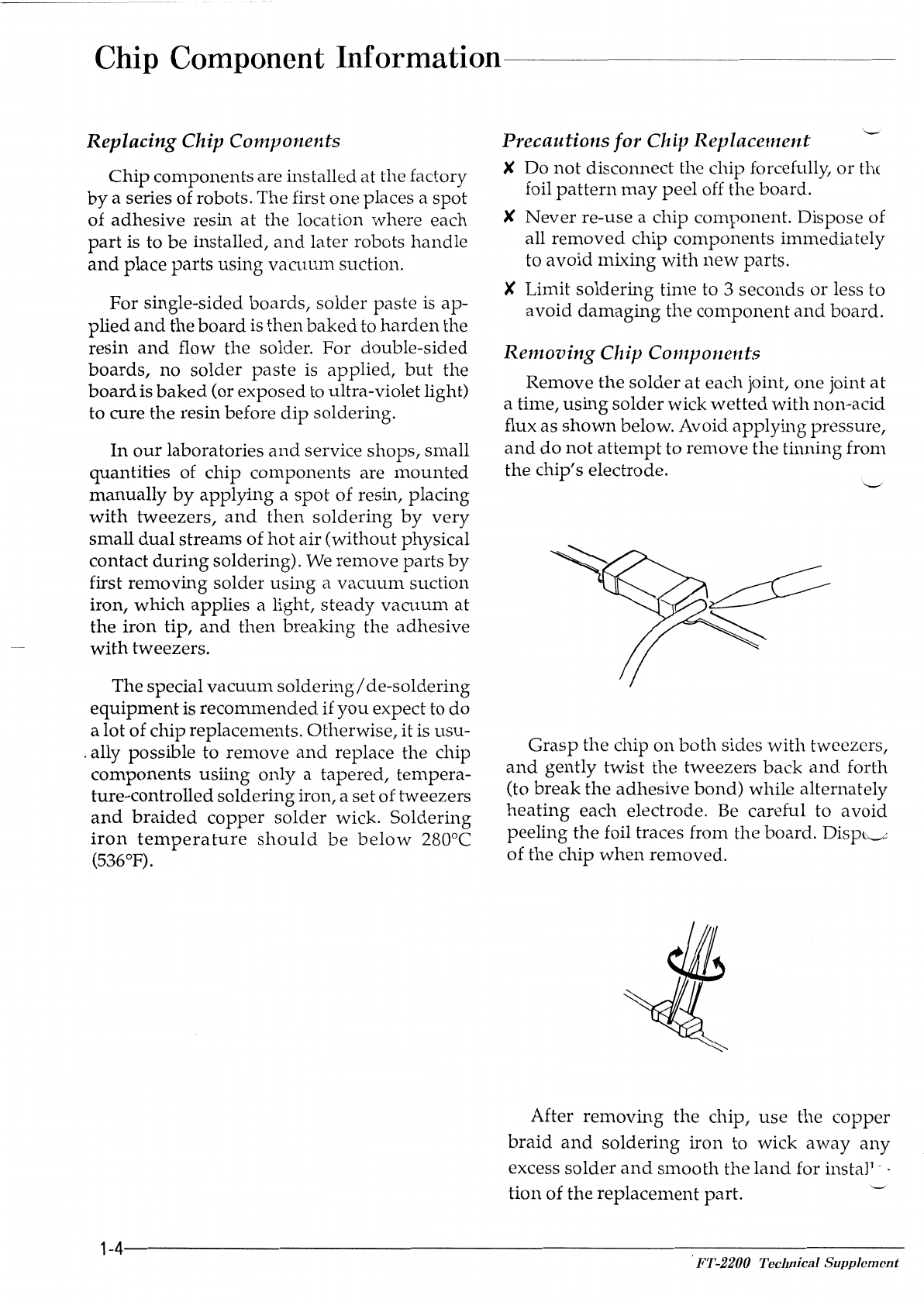
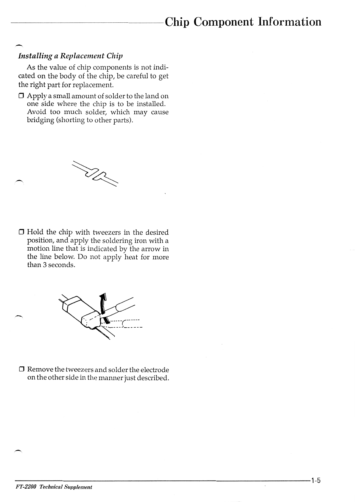
Yaesu FT-2200 Manual

FT-2200
TECHNICAL
SUPPLEMENT
YAESU
MUS
EN
CO., LTD.
C.P.O. Box 1500, Tokyo,
Japan
YAESU U.S.A.
17210
Edwards
Rd.,
Cerritos,
California
90701,
U.S.A.
YAESU
EUROPE
B.V.
Snipweg3.1118AA
Schipol,
The
Netherlands

-----------------
1.
General Information
Introduction . . . . . . .
Case Disassembly & PCB Access
Chip
Component
Information .
Circuit Description . . . .
Block
Diagram
. . . . . .
Interconnection
Diagram
2.
Servicing
Contents
LCD, CNTL Unit Access & Pilot
Lamp
Replacement .
Lithium Backup Battery Replacement
Alignment
............
.
PLL VCV & Reference Oscillator
Transmitter Deviation
.....
.
Receiver Interstage Transformers
Internal
System AlignmentRoutine
3. Board Unit's (Schematics,
Layout
& Parts)
IF
Unit
..
VCOUnit
APC Unit
MICAMPUnit
SRX-1
Unit.
PA Unit
..
LCD Unit
MUTE
Unit
MAIN
Unit
CNTL
Unit.
4.
Mechanical
Exploded
View
5. Accesson; Board Unit's (Specification,
Layout
& Parts)
FTS-27
CTCSS
Tone
Squelch
Unit
(option)
....
DVS-3 Digital Voice System
Unit
(option) . .
..
MW-2 Wireless Remote
Microphone
(accessory)
MH-26 series Microphone (accessory)
MH-27B8 Microphone (accessory)
........
.
-------~---
~
1-1
1-2
1-3
1-7
.
1-11
1-13
2-1
2-2
2-3
2-5-
2-5
2-6
2-7
3A-1
3B-1
3C-1
3D-1
3E-1
3F-1
3G-1
3I-I-1
. 3I-1
.
3J-1
................
4-1
SA-l
SB-1
5C-1
SD-1
SE-1
~

-------------------------------------Introduction
,-,.
The information in this manual is intended
to supplement the
FT-2200
Operating Manual,
for servicing the transceiver. Specifications
and
details of operation
and
options are provided
in the operating manual,
and
are not reprinted
herein. Therefore, the manual is not intended
to serve as
an
independent reference,
but
to be
used in conjunction with the information pro-
vided
in the operating manual. The
FT-2200
is
intended to
be
serviced only
by
qualified tech-
nicians.
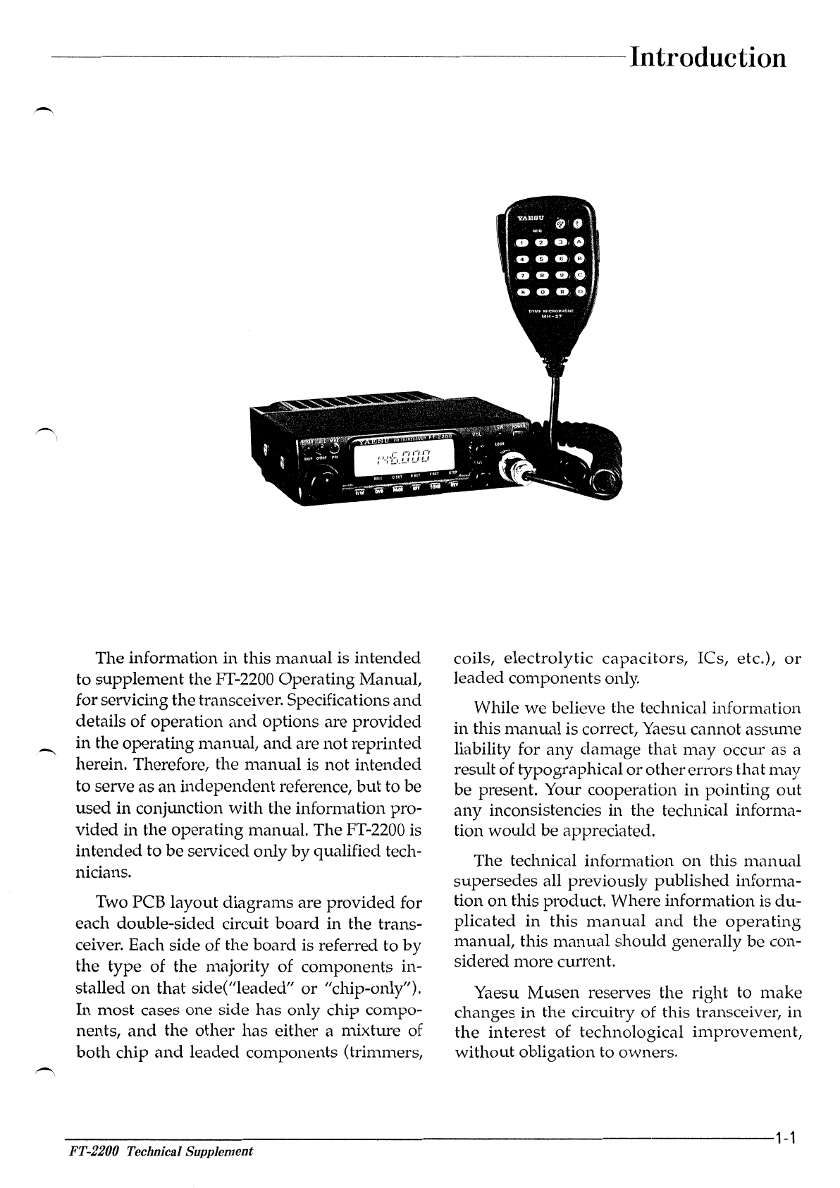
Two PCB layout diagrams are provided for
each double-sided circuit
board
in the trans-
ceiver. Each side of the board is referred to
by
the type of the majority of components in-
stalled on that side("leaded"
or
"chip-only").
In most cases one side has only chip compo-
nents,
and
the other has either a mixture of
both
chip
and
leaded components (trimmers,
coils, electrolytic
capacitors,
ICs, etc.),
or
leaded components only.
While
we
believe the technical information
in this manual is correct, Yaesu cannot assume
liability for
any
damage that
may
occur as a
result oftypographical
or
othererrorsthatmay
be present. Your cooperation
in
pointing
out
any
inconsistencies in the technical informa-
tion would be appreciated.
The technical information on this manual
supersedes all previously published informa-
tion
on
this product. Where information is
du-
plicated
in
this
manual
and
the
operating
manual, this manual should generally be con-
sidered more current.
Yaesu Musen reserves the right to make
changes
in
the circuitry of this transceiver, in
the
interest of technological
improvement,
without obligation to owners.
-----------------------------1-1
FT-2200 Technical Supplement

Case
Disassembly
& PCB
Access~~~~~-
Case
Disassembly
& PCB Access
Turn off
the
transceiver,
and
disconnect all
cables.
Main Unit
Access
(
top
&
botto1n)
0
Referring
to
figure
1,
remove
the
eight
screws from the
top
cover to expose the sol-
der
side of
the
Main
Unit.
0 Remove the four screws from
the
bottom
cover,
to
expose
the
component
(PCB
unit's) side of
the
Main
Unit
(Figure
2).
0
Unplug
the
speaker
wire connector from
Jl006
on
the
Main Unit,
and
lift
the
loud-
speaker
out
of it's bracket, as
shown
in Fig-
ure
3.
0
Remove
the
screw
affixing
the
speaker
bracket
and
remove
the
bracket.
PCB locations are indicated
in
Figure
4.
Figure
1.
MAIN
Unit
Figure
4.
Figure
2.
-~-IF
Unit
MUTE
Unit
'-'=*+--MIG
AMP
Unit
1-2------------------------------------------------~----------------
FT-2200
Technictll
Supplement

-----------Chip
Component Information
Chip ComponentInformation
The
diagrams
below
indicate
some
of
the
distinguishing
features
of
common
chip
com-
ponents.
Ceramic
Capacitors
Tantalum
Capacitors
Polarized.
Unmarked
(determine
value
from
layout
and
Parts
List)
Resistors
T
.-
Type
1/10
1/16
INDICATED LETTERS
1 2 3 4
5 &7 :
' D•
Type
3216
2125
1608
L
2.0
I. 6
L w
3.2
1.
6
2.0
1.
25
I. 6 0.8
w T
1.25
0.45
0.8 0.45
(Unit:
mm)
T
0.45~0.60
0.
35~0.
50
0.65~0.95
Type
RMC
1/lOW,
1/16W
Marking*
100,222,473·
..
···
1147311
____
.IJ
L-1
__
1
Ten
unit
0
1
2
3
4
5
6
7
8
9
One
unit
Multiplier
code
0
1
2
3
4
5
6
7
8
9
Examples:
100=10!1
222
= 2.2k!1
473
= 47k!1
1
0°
1
0'
102
103
1
o·
10
1
106
1
0'
108
1
og
--------------------------------------------------------------1-3
FT-2200 Teclmical Supplement

Chip
Component
Information~~~~~~--~~~~
Replacing Chip Components
Chip
components
are installedat the factory
by
a series
of
robots. The first
one
places a
spot
of
adhesive
resin
at
the location
where
each
part
is to
be
installed,
and
later
robots
handle
and
place
parts
using
vacuum
suction.
For single-sided
boards,
solder
paste
is
ap-
plied
and
the
board
is
then
baked
to
harden
the
resin
and
flow the solder. For double-sided
boards,
no
solder
paste
is
applied,
but
the
board
is
baked
(or
exposed
to ultra-violet light)
to cure
the
resin before
dip
soldering.
In
our
laboratories
and
service
shops,
small
quantities of chip
components
are
mounted
manually
by
applying
a
spot
of
resin, placing
with
tweezers,
and
then
soldering
by
very
small
dual
streams
of
hot
air
(without
physical
contact
during
soldering).
We
remove
parts
by
first
removing
solder
using
a
vacuum
suction
iron,
which
applies a light,
steady
vacuum
at
the
iron
tip,
and
then
breaking
the
adhesive
with
tweezers.
Thespecial
vacuum
soldering/
de-soldering
equipment
is
recommended
if
you
expect to
do
a lot ofchip replacements. Otherwise,
it
is
usu-
.ally possible to
remove
and
replace the chip
components
usiing
only
a
tapered,
tempera-
ture-controlled
soldering
iron, a setoftweezers
and
braided
copper
solder
wick.
Soldering
iron
temperature
should
be
below
280°C
(536°F).
Precautions for Chip Replacement
X Do
not
disconnect the chip forcefully,
or
the
foil
pattern
may
peel
off the
board.
X
Never
re-use a chip component. Dispose of
all
removed
chip
components
immediately
to
avoid
mixing
with
new
parts.
X Limit
soldering
time
to 3 seconds
or
less to
avoid
damaging
the
component
and
board.
Removing
Chip Components
Remove
the
solder
at
each joint,
one
joint
at
a time,
using
solder
wick
wetted
with
non-acid
flux as
shown
below. Avoid
applying
pressure,
and
do
not
attempt
to
remove
the
tinning
from
the chip's electrode.
Grasp
the
chip
on
both
sides
with
tweezers,
and
gently
twist
the
tweezers
back
and
forth
(to
break
the
adhesive
bond)
while alternately
heating
each
electrode.
Be
careful to
avoid
peeling
the
foil traces from the board.
Displ~
of
the chip
when
removed.
After
removing
the
chip,
use
the
copper
braid
and
soldering
iron
to wick
away
any
excess
solder
and
smooth
the
land
for instaP- ·
tion
of
the
replacement
part.
1-4----------------------------------------------------------
·
FT-2200
Teclmical
Supplement

------------Chip
Component Information
-
Installing a Replacement Chip
As the
value
of chip components
is
not
indi-
cated
on
the
body
of
the
chip,
be
careful to get
the
right
part
for replacement.
0
Apply
a small
amount
of
solder
to the
land
on
one side
where
the chip is to be installed.
Avoid too
much
solder,
which
may
cause
bridging
(shorting to
other
parts).
0
Hold
the chip
with
tweezers in
the
desired
position,
and
apply
the soldering iron
with
a
motion
line
that
is indicated
by
the
arrow
in
the line below.
Do
not
apply
heat
for
more
than
3 seconds.
0 Remove thetweezers
and
solderthe electrode
on
the
other
side
in
the
manner
justdescribed.
---------------------------------------------------------------1-5
FT-2200 Technical Supplement

Notes~~~~~~~~~~~------
1-6--------------------------------------------------------------~JV1T1'~-2~2WO~O~~;.ec~h~nd.k~a~JtS~u~p~plke~n~le~n1t

----------------Circuit
Description
~Receive
Signal Path
Incoming
RF
from
the
antenna
jack is deliv-
ered
to the PA
Unit
and
passes
through
a low-
pass
filter consisting of coils L703 & L704,
capacitorsC712 & C713
and
antenna
switching
diodes,
D703 & D704
(both
Ml308) to
the
MAll\i l.Jnit.
Signals
within
the
trequency
range
of
the
transceiver
then
enter
a varactor-
tuned
band
pass
filter
consisting
of
diode
D1012
(1
T326) & T1005 before RF amplifica-
tion
by
Q1004 (3SK131).
The
amplified
RF is
then
varactor-tuned
band
pass filtered
again
by
diodes
D1005, D1006, D1007 & D1008 (all
1T362)
and
T1003, T1004, T1006 & T1007 be-
fore
impedance
matching
by
T1001
and
enter-
~ing
the
1st
mixer
Q1001
&
Q1003
(both
2SK302).
Buffered
output
from
the
VCO
Unit
is
am-
plified
by
Q1011 (2SC2759) to
provide
a
pure
1st local signal
between
126.3
and
130.3MHz
for injection to
the
1st
mixer. The 17.7-MHz 1st
mixer
product
then
passes
through
dual
mono-
lithic crystal filters XF1001 & XF1002 (both
17T15BU:
±7.5
kHz
BW)
to
strip
away
all
but
the
desired
signal,
which
is
then
amplified
by
Q1002 (2SC2620).
The
amplified
1st IF signal is
applied
to FM
IF
subsystemIC
Q201 (MC3372ML)
on
the
IF
Unit,
which
contains
the
2nd
mixer,
2nd
local
oscillator, limiter amplifier, noise amplifier,
S-
,-.,meter
amplifier
and
squelch
gates. A
2nd
local
signal
is
generated
from
17.245MHz crystal
X201, to
produce
the
455kHz
2nd
IF
when
mixed
with
the
1st IF signal
within
Q201. The
2nd
IF
then
passes
through
ceramic filter
CF
1001 (CFW455E)
on
the
MAIN
Unit, to
strip
away
unwanted
mixer
products,
and
is
then
returned
to
the
IF
Unit
and
applied
to the
limiter amplifier
in
Q201,
which
removes
am-
plitude
variations
in
the
455kHz
IF,
before
de-
tection of
the
speech
by
ceramic
discriminator
CD201 (CDB455C7).
Detected
audio
from
Q201 is
fed
through
mute
analog
switch
Q906 (2SC2812)
on
the
MUTE Unit
and
then
enters
the
MIC
AMP
UNIT
for
de-emphasis,
high-and
low-
pass
fil-
tering
by
Q501 (NJM2902M-1, -3)
on
the MIC-
AMP
Unit before
returning
to
the
MAIN
Unit.
Audio
output
levelis
controlled
by
VOL
poten-
tiometer
VR2002
on
the CNTL
Unit
and
audio
amplifier Q1020 (AN5262) before application
to
audio
power
amplifierQ1021 (TDA2003) for
up
to 2
watts
for
the
optional
headphone
jack
or
8-ohm
loudspeaker.
Squelch Control
The
squelch
circuitry consists ofa noise
am-
plifier,
high-pass
filter &
squelch
trigger
within
Q201,
and
noise
detector
D201
(1
SS302),
both
on
the
IF Unit,
squelch
gate
Q506
on
the MIC-
AMP
Unit,
and
control
circuitry
within
micro-
processor Q2001 (HD4074629H)
on
the CNTL
Unit.
When
no
carrier is received, noise
at
the
output
of
the
detector stage of Q201 (pin
11)
is
detected
by
D201
(1
SS302)
to
provide
a DC
control
voltage
for squelch
gate
control. This
voltage
is
delivered
to NOISE/I-I TEMP
pin
2
of Q2001
on
the
CNTL Unit. With no carrier
present,
pin
2 of Q2001 is
high
which
signals
the
microprocessor
to activate
squelch
gate
Q506
(DTC323TK)
on
the
MIC-AMP
Unit,
pulling
the
audio
line to
ground,
thus
silencing
the
receiver
while
no
signal
is
being
received.
Transmit Signal Path
Speech
input
from
the
microphone
is deliv-
ered
via
the
CNTL
Unit
to
the
MIC-AMP Unit,
where
it
passes
through
Mic Amplifier Q501
(NJM2902M-4)
and
Mic
Mute
analog
switch
Q503 (UPD4052BG).
To
prevent
over-devia-
tion,
the
audio
is
processed
by
IDC (instantane-
ous
deviation
control) Q501 (NJM2902M-2),
and
then
low-pass
filtered
by
Q501
(NJM2902M-3) before
delivery
to
the
modula-
tor
on
the
VCO Unit.
If
a CTCSS
tone
is
enabled
for transmission,
the
subaudible
tone
from
microprocessor
Q2001
on
the
Control
Unit
is
lowpass
filtered
-------------------~--------------------------~---------1-7
FT-2200 Technical Supplement

Circuit
Description---------
by
Q2013 (NJM2902M-3)
and
mixed
with
the
IDC-processed
speech
audio.
Also,
DTMF
tones
from
the
microprocessor are
applied
to
the
transmit
audio
chain
at
the
input
of
the
IDC
stage. The microprocessor also disables micro-
phone
audio
at
Mic
Mute
analog
switch Q503
via
Q505 (UPD4094BG)
when
necessary.
The
modulated
audio
is
delivered
to varac-
tor
diodes
D303 & D304 (Both 1T363)
on
the
VCO
Unit, frequency
modulating
the
PLL car-
rier
up
to±
5kHz
from the
unmodulated
car-
rier
at
the
transmitting
frequency.
The
modulated
signal
from
transmitter
VCO Q303
(2SC4226) is buffered
by
Q305 (2SC2759)
and
delivered
to
the
Main
Unit
for amplification
by
Q1010 (2SC2759), Q1009 (MMBR951
L)
and
Q1008 (2SC2538). The low-level
transmit
sig-
nal
is
then
applied
to
the
PA
Unit,
where
it is
finally
amplified
by
PA
module
Q701
(M67781
L)
up
to 50
watts
output
power.
The
transmit
signal
then
passes
through
antenna
switch
D702 (UM9415)
and
is
low-pass filtered
to
suppress
away
harmonic
spurious
radiation
before
delivery
to the
antenna.
Automatic
Transmit
Power
Control
RF
power
output
from
the final amplifier is
sampled
by
C715
and
rectified
by
D705
(1
SS97)
on
the
PA Unit. The
resulting
DC is
passed
through
high/medium/low
power
controller Q404 (FMS1)
on
the
APC
Unit
to
Automatic
Power
Controller
Q1012
(2SB1134S)
on
the
MAIN
Unit,
which
regu-
lates
supply
voltage
to
transmitter
RF amplifi-
ers Q1008
and
Q701, to
maintain
stable
high,
medium
or
low
output
power
under
varying
antenna
loading
conditions.
Spurious Suppression
Generation
of
spurious
products
by
the
transmitter
is
minimized
by
the
fundamental
carrier
frequency
being
equal
to the final trans-
mitting
frequency, m.odulated directly
in
the
transmit
VCO.
Additional
harmonic
suppres-
sion
is
provided
by
low-pass
filter consisting of
L701, L704, L705
and
C706, C707, C708, C713,
C714,C722
and
C723,
resulting
in
more
than
60
dB of
harmonic
suppression
(for
transmitting'-
frequencies
in
the
amateur
band)
prior
to de-
livery to
the
antenna.
PLL Frequency
Synthesizer
PLL circuitry
on
the 1vfain Unit consists
o£
PLL
subsystem
IC Q1016 (MB1504),
which
contains a reference oscillatorIdivider, serial-
to-parallel
data
latch,
programmable
divider
and
a
phase
comparator.
Stability is
main-
tained
by
a
regulated
5-V
supply
via Q1018
(UPD7805H) to Q1016
and
temperature
com-
pensating
capacitors associated
with
12.8
MHz
frequency
reference crystal X1001.
Receiver VCO Q301 (2SC4226)
on
the
VCG-
Unit
oscillates
between
126.3
MI-Iz
and
130.3MHz
according
to
the
programmed
re-
ceiving frequency.
The
VCO
output
is
buffered
by
Q305 (2SC2759)
on
the
VCO Unit,
and
then
returned
to
the
Main
Unit
where
a
sample
of
the
output
is
buffered
by
Q1015 (2SC2714) for
application
to
the
prescalar
/swallow
counter
section
of
Q1016. There
the
VCO
signal
is di-
vided
by
64
or
65,
according
to a
control
signal
from
the
data
latch
section of Q1016, before
being
applied
to the
programmable
divider
section in
the
PLL chip.
The
data
latch section of Q1016 also receives
serial
dividing
data
from
microprocessor
Q2001
on
the
Control
Unit,
which
causes
the
pre-divided
VCO
signal
to
be
further
divided'-"
by
25260 to 26060
in
the
programmable
divider
section,
depending
upon
the
desired
receive
frequency, so as to
produce
a 5
kHz
or
6.25
kHz
derivative
of
the
current
VCO
frequency.
Meanwhile,
the
reference
divider
section
in
Q1016
divides
the
12.8 MI-Iz crystal reference
by
2560 (or 2048) to
produce
the
5kHz
(or 6.25
kHz)
loop
reference (respectively).
The
5
kHz
(or 6.25
kHz)
signal
from
the
programmable
divider
(derived
from
the
VCO)
and
that
derived
from the crystal are
applied
to
the
phase
detector
section
in
Q1016,
which
produces
a
dualS
V
pulsed
output
with
pulse
duration
depending
on
the
phase
differ-
ence
between
the
input
signals.This
pulse
trair\-/
1-8--------------------------------------------------------------------
FT-2200 Teclmical Supplement

----------------Circuit
Description
~
is converted to DC
by
charge
pump
section of
Q1016,
and
is
then
fed
through
the low-pass
filter to varactors D301 to D304 (both 1T363)
on
the VCO Unit.
Changes
in
the level of the
DC
voltage
ap-
pliedto D301 & D302 affect thereactance in the
tank
circuit of Receiver VCO Q301, changing
the
oscillating
frequency
according
to
the
phase
difference
between
the
signals
derived
from the VCO
and
the crystalreference oscilla-
tor. TheVCO is
thus
phase-lockedto thecrystal
reference oscillator.
The
output
ofreceiverVCOQ301, afterbuff-
ering
by
Q305, is deliveredto the Main Unitfor
~.
amplification
by
Q1011
(2SC2759) before
ap-
plication to the 1st mixer, as described pre-
viously.
TransmitterVCO Q303 (2SC4226) oscillates
between
144
MHz
and
148
MHz
according to
the
programmed
transmit frequency. The re-
mainder
of the PLL circuitry is
shared
with
the
receiver. However, the dividing
data
from the
microprocessoris such that theVCO frequency
is
at
the actual transmit frequency (rather
than
offsetfor IFs,as
in
the receiving case). Also, the
transmitter VCO is
modulated
by
de-empha-
sized
audio
applied
to D303 & D304, as de-
scribed previously.
Transmit Inhibit
When
the transmit PLL is unlocked
pin
7 of
PLL chip Q1016 goes to a logic low, turning on
Q1017, Q405
and
Q401,
which
then
turns
off
Automatic
Power
Controller Q401
and
Q1012
to disable
the
supply
voltage to transmitterRF
amplifiers
Q1008
and
Q701,
disabling
the
transmitter.
Miscella~teous
Circuits
Push-To-Talk
Transmit
Activation
The
PIT
switch
on
the
microphone is con-
nected to
pin
21
of microprocessor Q2001, so
that
when
the
PIT
switch is closed,
pin
21
of
Q2001 goes low. This signals microprocessor to
activate TX/RX controller Q408 (2SC2812)
on
the
APC Unit,
which
then
disables the receiver
by
disabling
the
9V
supply
bus
at
Q402
(288624)
to the front-end,
IF,
discriminator
and
receiver VCO circuitry. At the
same
time,
Q403
(288624)
activates the transmit 9 V
sup-
ply
line to enable the transmitter.
--------------------------------------------------------------1-9
FT-2200 Technical Supplement

Notes----------------~
1-10-------------------------------------------------------------F~1~~2~~~00~T,r.e;chhn;;i;ca~l~S~'u~p~phk~n~Je~ntt

~-------------

~---------------------------------------
MAIN-UNIT
F3343000A
~--------------,
I
SRX
I
-UNIT
I
I
I
F3345101A
I TUN v
AMP
BUFF
I
I
._
_____________
_j
L-----------------.
I
I
·-
'
I
'
--"
I
TSlOOl
I
OHD-BOM
1-------------------
THERMAL
SW
APC t
----------f-----1
I
VCO-UNIT
:
I F3347101
,f,
I
I I
I
I
I
I
I
I
---t------J!
·:::::_-
i-::_-::_-::_-::_-::_-::_T
~
I
~-;:::::::J==:;-~vcv:=:::L--,
,----------------,
LCD-UNIT
I
I F33461
01
A I
I
I
I
I
I
I
I
SEG
QBOl
COM
LC7582E
LCD
OR
I VE
I I
I
._
_______________
j
TX
LINE
..
-----•·
RX
LINE
COMMON
LINE--------
FT-2200 Tecllnical Supplement
l_----~----~L~D~W---~========1
VOL.S
CK
DATA
CPU
Q2001
HD4074629H
I
I
L
_____________________
_

------------------Block
Diagram
---~--------------------------------------------~
LO
fu
XFIOOI.
2
I
7TI
SBU
-~-J
~--------------,
!IF-UNIT
Q201
I
IF33481
04
MC3372ML
FM
IC
I
I
I
I
I
I
_
_j
~-------------
MUTE-UNIT
I
F334B
I
05
I
I
I I
I
I
I
I
L
_____________
_j
r
~c-AMP-uNIT
I F3348101
I
L-
--}:.:.
~-~=-=.--.:.._-::.:.:.
-:__-=
:.=_-_:.-~--..:_-~~
=.-:::
:_:--
FILTER
CFW455E
'
' '
~--------~------·J
____
_.__
____
_
'
,
'
J-----------
-------~----
TONE
I
~---
v,---~o--
,.-------,---l----4------+---l
TDET
TONE
-SQL
-UNIT
I
FTS-27 1 DVS-UNIT
I DVS-3
noos-7
02005-8
FMG2
IMNIO
BAND
TABLE
(OPT
I
ONl
I
I
CK
I
I
DATA
----
_2:
SQL_---
_I
'
L
-------:------
L--------f--,
Q2012
TC3505F
DTMF
DECODER
'
I
I
I
I
I
I
I
I
I
I
-------------------~
(OPT
I
ONl
I
CK
I
I
DATA
____
__!STB
____
j
hx""1Rx
=144~148MHz
11FI=
17.7MHz
fu
...
rl'lx-11F1
fiF2"'455kH:z
_______
_j
-----------------------------------------------------------------1-11

~;--UN;;---,
I
F3346101A
I
.---
1
MAl
I
I
I
(NO.
B**l
I
I
J801
I I
J1001
SP.
STB
1'>+-1---------+-H
I
'H-1--H{
I
DATA
I
I
I
I
I
DIM
5V
GND
L
_____
_j
,-----,
I
VOICE-MEMORY
I
-UNIT
JP101
(OPTION)
DVS-3
OS
P2
Pi
TOE
DATA
DIM
5V
rnH
GND
CE
)-HI---f-+(7
PAGSTB
ACe
VSTB
UP
5V
u
H
::.:
P.STB
T.STB
CK
T-DET
NC
DTMF/BZ
MIC
H
TEMP/NOISE
VOL
SP
J2004
PTT
I
I
I
I
I
I
DOWN
ACC
I
\.I-I----.LJ.(6
DATA
!EEl
I
\.1-1----.J..+I
7
CK
I
I
TOP
VIEW
L_
____________
j
FT-2200 Technical Supplement
T-DET
NC
DTMF/BZ
UL
MIC
ENC
9V
SIG
DISC
H
TEMP/NOi
J1005
GND
VOL
SP
13-8
13US
5V
0
>

---------------Interconnection
Diagram
-------------~
~-UNIT
F3343000A
(NO.
1***)
I
r-------,
1 VCO-UNIT 1
I
F3347101
I
L
(NO.3**)
J
I
I
i--------~
PlOOl
Jl0071
~J702
JP~!
{\
I T9205644
------
~--IF-UNIT--l
I
F3348104
I
'--~0~2**_)
_j
T9~
~
1
T9
ANT
hi
~
[AN]l
APC
2
-----
2
APC
I
AFP
3 3
AFP
I
JlOlO
IP021
I I
JP702
I
~
_
Pl003
T9317910
~
TX
IN
~-
~'ic-AMP-UNITJ
I
F3348101
I
TX
IN~
I I
't___5
I
Jl009(P011
I I
JP703
I
J703
"''"~
i
""'"
T9317909 L
~'"
~·
,:;rrv
n
I>><
op:
L-~~**l
__
j
GND
r-------,
'E
I APC-UNIT I
,I
F3348102
I
VCON
-'1
1--------y
-'1
\ICON
I
'--~~4**l
__
j
r---------,
I I
GND
I I I
P1005
T9206261
I I I
I MUTE-UNIT I
I
F3348105
I
L
(N0.9**)
j I I I
I PA-UNIT
F3344101A
I
I
(N0.7**)
I
------
r---------,
I SRX1-UNIT I
I
F3348103
I
~--~O~**l
__
j
J1003
...-t-+--t-t--t-----Jr-t-----±8~
O:::t::t-<(ffi_j>W
I
(5U~~5~U1§
I
I TONE-SQL-UNIT I
I (OPTION) I
FTS-27
L
_______
_l
1_
_______
1
-------------------------------------------------------------1-13


---LCD,
CNTL
Unit
Access
& Pilot
Lamp
Replacement
-_
LCD and Control
Unit
Access
0
To
access
the
Control
Unit
and
LCD,
remove
the
VOL, SQL
and
DIAL
knobs
by
gently
pulling
them
outward.
0
Remove
the
two
screws
as
shown
in Figure
5,
then
unscrew
the
ring
nut
affixing
the
mic
jack
(you
may
be
able to
do
this carefully
using
a
pair
of
long-nose pliers,
or
have
your
dealer
do
this
with
a special wrench).
0
Again
using
a
pair
of
long
nose pliers, re-
move
the
nut
from
the
DIAL
knob
shaft.
Remove
the
front
panel
and
LCD
Unit
by
gently
pulling
it
away
from
the
transceiver
body.
Note
the
small
connector
on
the
rear
of the LCD
Unit
that
mates
with
jack J2006
on
the
Control
Unit
circuit
board
(Figure 6).
Pilot
Lamp Replacement
With
the
rear
of
the
front
panel
exposed,
the
four
LCD
backlighting
lamps
are
accessible
(Figure
6).
Use
a
low-wattage
soldering
iron
to
remove
the
lamps
and
install
new
ones.
Control
Unit
Jumper Settings
From
the
factory,
pin
5 of the
microphone
jack is
wired
to
enable
certain functions
by
pressing
the
D/MR
or
CALL
button
on
the
sup-
plied
microphone.
The
function selectable dif-
fers
according
to transceiver
version
type,
as
configured
by
jumper
settings
on
the
front
of
the
Control
Unit
PCB (see Figure 7
at
the
right
,-.,
and
Table 1
on
the
next
page).
-
Squelch
Status/
Packet TNC Modification
Most
packet
TNCs
can
be
connected
to
the
FT-2200
as
outlined
in
the
Operation
Manual,
however,
some
earlier
model
TNCs
require
a
Squelch
Status
indication
from
the
transceiver
for
operation.
If
your
unit
is this
type,
you
can
modify
a
jumper
setting
for this
indication
via
pin
5
of
the
mic. jack.
However,
please
confirm
this
in
the
documentation
supplied
with
the
TNC
before
performing
the
modification.
Figure
5.
Figure
6.
Figure
7.
--------------------------------------------------------------2-1
FT-2200 Technical Supplement

Lithium
Backup
Battery
Replacement---
Table 1. Accessory
Jumper
Settings
JMP8
JMP9
JMP Function
10
Toggle DIAUMemory Mode
• Toggle CALL Channel
•
1750Hz
Tone Burst
• • Monitor (Squelch Disable)
• Squelch Status (channel busy)
"
~"
denotes installed jumper.
Figure
8.
0 0
..
:1:
' 0 0
Figure
9.
0
Note
the location of
jumper
pads
8, 9 & 10
on
the
bottom
left of
the
front
of
the
Contr'-#
Unit
PCB (Figure 7).
0 Usinga low-wattage solderingiron,
solder
a.
0-KQ
chip
resistor
or
jumper
wireacross
pad
10. Do
not
jumper
the
pad
by
forming a
solder bridge!
Control Unit PCB
Renwval
0 With
the
Front Panel
removed
and
Control
Unitexposed,
remove
the three screws affix-
ing
the Control
Unit
PCB to
the
front of
the
transceiverchassis,
then
remove
the Control
Unit
using
both
hands
to gently evenly
pull
it
away
from
the
front
of
the
Main
Unit PCB
and
transceiver
chassis.
Note
how
jackr
J2001
&J2002
on
the
rear
of
the
Control
U~'-"
mate
with
the
corresponding
connectors
on
the
Main
Unit,
use
these
as
alignment
guides
when
re-installing
the
Control
Unit
PCB (Figure 8).
Lithium Battery Replacement
0 With the Control
Unit
removed
from th
chassis,
locate
Lithium
Backup
Battery
BT2001(P/N
09000552)
on
the
rear
side of
the
PCB (Figure
9).
Note
the
polarity
and
correct
mounting
of
the
cell terminals. Un-
solder
the
battery
terminals
and
remove
the
old cell. Note:
do
not
dispose of
the
old
battery
in
fire,
and
ensure
small children
cannot
play
with,
or
possiblyingest
the
c·
'-"
0 Install
the
insulating seals (P/N R8118690)
on
each side
of
the
battery
by
peeling
back
the
adhesive
covering
and
sticking one to
each side
of
the
cell (below Figure 10).
Backup
Battery
Figure
10.
2-2-----------------------------------------------------------------
FT-2200 Teclmical Suppleme11t
Other manuals for FT-2200
1
Table of contents
Other Yaesu Transceiver manuals

Yaesu
Yaesu FT-710 Use and care manual

Yaesu
Yaesu FT-2000 - MENU MODE LIST User manual

Yaesu
Yaesu FT-991 User manual

Yaesu
Yaesu FT-817 - Manual

Yaesu
Yaesu FT-60R User manual

Yaesu
Yaesu FT-757GX II User manual

Yaesu
Yaesu FT-847 User manual

Yaesu
Yaesu FT DX 9000 CONTEST - 2 Manual

Yaesu
Yaesu VX-120 Series User manual

Yaesu
Yaesu FT-73R User manual

Yaesu
Yaesu FT-2000 - MENU MODE LIST Product guide

Yaesu
Yaesu GX1280S User manual

Yaesu
Yaesu FT-26 Manual

Yaesu
Yaesu FT DX 3000 User manual

Yaesu
Yaesu FT-1907R User manual

Yaesu
Yaesu FT-897 User manual

Yaesu
Yaesu FTDX 9000 Series User manual

Yaesu
Yaesu FT5Dr User manual

Yaesu
Yaesu FT-102 User manual

Yaesu
Yaesu VX-6R User manual