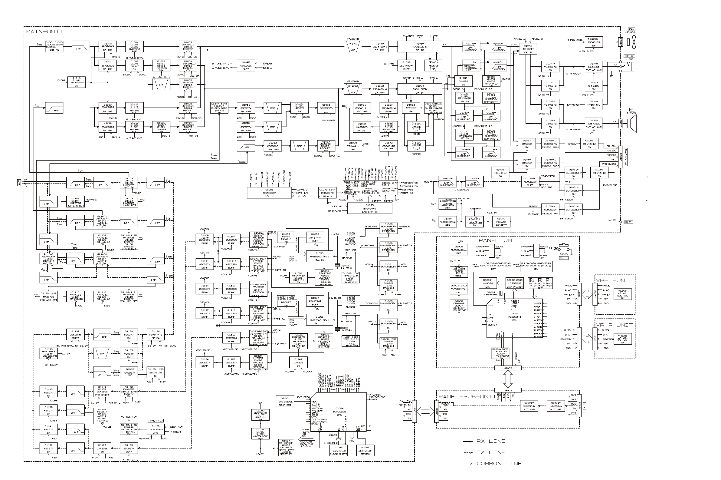
8
Q1130 (NJM2904V), as a DC voltage which is proportional
to the output level of the power amplifier.
AtQ1130, the rectified DC voltage from the power am-
plifier is compared to the reference voltage from the main
CPU Q1084 to produce a control voltage, which regulates
supply voltage to the pre-drive amplifier Q1123
(2SK5374), driver amplifier Q1137 (2SK2975),and pow-
er amplifier Q1134 (RD70HVF1), so as to maintain stable
output power under varying antenna loading conditions.
29 MHz
A portion of the Power amplifier output is rectified by
D1120 and D1122 (both MA2S728) then delivered to APC
Q1130 (NJM2904V), as a DC voltage which is proportional
to the output level of the power amplifier.
At Q1130, the rectified DC voltage from the power am-
plifier is compared to the reference voltage from the main
CPU Q1084 to produce a control voltage, which regulates
supply voltage to the pre-drive amplifier Q1123
(2SK5374), driver amplifier Q1137 (2SK2975),and pow-
er amplifier Q1134 (RD70HVF1), so as to maintain stable
output power under varying antenna loading conditions.
PTT (Push to Talk) Circuit
430 MHz
When the PTT switch is pressed, pin 8 of sub CPU Q2001
(M38223E4HP) goes “high,” which sendsthe “PTT” com-
mand to main CPU Q1084.
When the “PTT” command is received, the main CPU con-
trolsthe I/O IC Q1075 (BU2090FS), causing pin 12 of
Q1075 to go “low” which activatesthe UHF TX switch
section of Q1076 (IMT17).
When the UHF TX switch section of Q1076 is activated, it
controls the antenna switch diodes D1102, D1104, and
D1146 (all UM9957F), modulator switching diode D1100
(DAN222),modulatorswitchingICQ1051(BU4066BCFV),
diode switches D1073 (HSC277), D1128 (DAN235E),
D1140 (HSC277), and D1134 (HSC277), and APC switch-
es Q1128 (RT1N441U) and Q1129 (RT1P441U), which ac-
tivate the 430 MHz transmitter circuit.
144 MHz
When the PTT switch is pressed, pin 8 of sub CPU Q2001
(M38223E4HP) goes “high,” which sendsthe “PTT” com-
mand to main CPU Q1084.
When the “PTT” command is received, the main CPU con-
trolsthe I/O IC Q1075 (BU2090FS), causing pin 13 of
Q1075 to go “low” which activatesthe VHF TX switch
section of Q1076 (IMT17).
When the VHF TX switch section of Q1076 is activated, it
controlsthe antenna switching relay RL1001 (G5A-237P),
modulator switching diode D1100 (DAN222), modulator
switching IC Q1051 (BU4066BCFV), diode switches
D1075 (HSC277), D1128 (DAN235E), D1139 (HSC277),
and D1133 (RSL135), and APC switches Q1128
(RT1N441U) and Q1129 (RT1P441U), which activate the
144 MHz transmitter circuit.
50 MHz
When the PTT switch is pressed, pin 8 of sub CPU Q2001
(M38223E4HP) goes “high,” which sendsthe “PTT” com-
mand to the main CPU Q1084.
When the “PTT” command is received, the main CPU con-
trolsthe I/O IC Q1075 (BU2090FS), causing pin 14 of
Q1075 to go “low” which activatesthe TX50 switch sec-
tion of Q1077 (IMT17).
When the TX50 switch section of Q1076 is activated, it con-
trols the antenna switching relayRL1002 (G5A-237P), mod-
ulator switching diodeD1092 (DAN222), modulator switch-
ing IC Q1086 (BU4066BCFV), diode switches D1127
(DAN235E),D1141(HSC277),andD1132 (D1F20),andAPC
switches Q1128 (RT1N441U) and Q1129 (RT1P441U),
which activate the 50 MHz transmitter circuit.
28 MHz
When the PTT switch is pressed, pin 8 of sub CPU Q2001
(M38223E4HP) goes “high,” which sendsthe “PTT” com-
mand to the main CPU Q1084.
When the “PTT” command is received, the main CPU con-
trolsthe I/O IC Q1075 (BU2090FS), causing pin 15 of
Q1075 to go “low” which activatesthe TX29 switch sec-
tion of Q1077 (IMT17).
When the TX29 switch section of Q1076 is activated, it con-
trols the antenna switching relayRL1003 (G5A-237P), mod-
ulator switching diodeD1092 (DAN222), modulator switch-
ing IC Q1086 (BU4066BCFV), diode switches D1127
(DAN235E),D1142(HSC277),andD1132 (D1F20),andAPC
switches Q1128 (RT1N441U) and Q1129 (RT1P441U),
which activate the 28 MHz transmitter circuit.
PLL Circuit
“Left” band
A portion of the output from UHF-VCO/A Q1112
(2SC5006) is passed through buffer amplifier Q1113
(2SC5374) and diode switch D1084 (HSC277) to the pro-
grammable divider section of the PLL IC Q1095
(MB15A02PFV1), where it is divided according to the fre-
quency dividing data associated with the operating fre-
quency input from the main CPU Q1084. It is then sent to
the phase comparator.
A portion of the output from the VHF-VCO/A Q1115
(2SC5374) is passed through buffer amplifier Q1116
(2SC5374) and diode switch D1089 (HSC277) to the pro-
grammable divider section of the PLL IC Q1095, where it
Circuit Description