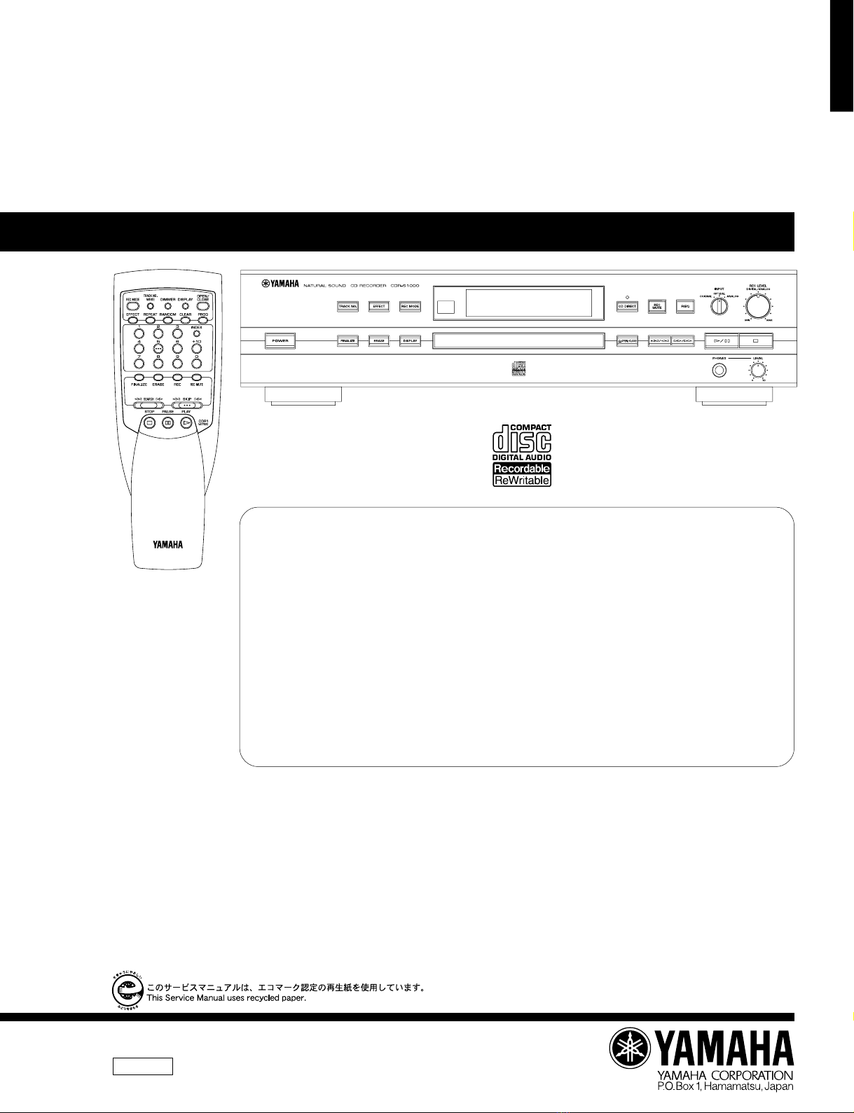
Yamaha CDR-S1000 User manual

CDR-S1000
CDR-S1000
100701
SERVICE MANUAL
CDR-S1000
IMPORTANT NOTICE
This manual has been provided for the use of authorized YAMAHA Retailers and their service personnel.
It has been assumed that basic service procedures inherant to the industry, and more specifically YAMAHA Products, are already
known and understood by the users, and have therefore not been restated.
WARNING: Failure to follow appropriate service and safety procedures when servicing this product may result in personal
injury, destruction of expensive components and failure of the product to perform as specified. For these reasons,
we advise all YAMAHA product owners that all service required should be performed by an authorized
YAMAHA Retailer or the appointed service representative.
IMPORTANT: The presentation or sale of this manual to any individual or firm does not constitute authorization, certification or
recognition of any applicable technical capabilities, or establish a principle-agent relationship of any form.
The data provided is believed to be accurate and applicable to the unit(s) indicated on the cover. The research, engineering, and
service departments of YAMAHA are continually striving to improve YAMAHA products. Modifications are, therefore, inevitable
and specifications are subject to change without notice or obligation to retrofit. Should any discrepancy appear to exist, please contact
the distributor's Service Division.
WARNING: Static discharges can destroy expensive components. Discharge any static electricity your body may have accumu-
lated by grounding yourself to the ground buss in the unit (heavy gauge black wires connect to this buss).
IMPORTANT: Turn the unit OFF during disassembly and parts replacement. Recheck all work before you apply power to the unit.
IC DATA .............................................................. 14—24
PIN CONNECTION DIAGRAM...................................25
PRINTED CIRCUIT BOARD .............................. 26—33
BLOCK DIAGRAM.............................................. 34—35
SCHEMATIC DIAGRAM..................................... 36—39
REMOTE CONTROL TRANSMITTER .......................40
PARTS LIST........................................................ 41—50
■ CONTENTS
TO SERVICE PERSONNEL................................... 1—2
REAR PANELS.............................................................3
SPECIFICATIONS.........................................................4
INTERNAL VIEW ..........................................................5
DISASSEMBLY PROCEDURES ............................ 5—7
SERVICE CHECK PROCEDURES ........................ 8—9
TEST PROGRAM................................................ 10—13
COMPACT DISC RECORDER

CDR-S1000
CDR-S1000
1
AC LEAKAGE
TESTER OR
EQUIVALENT
EQUIPMENT
UNDER TEST
INSULATING
TABLE
WALL
OUTLET
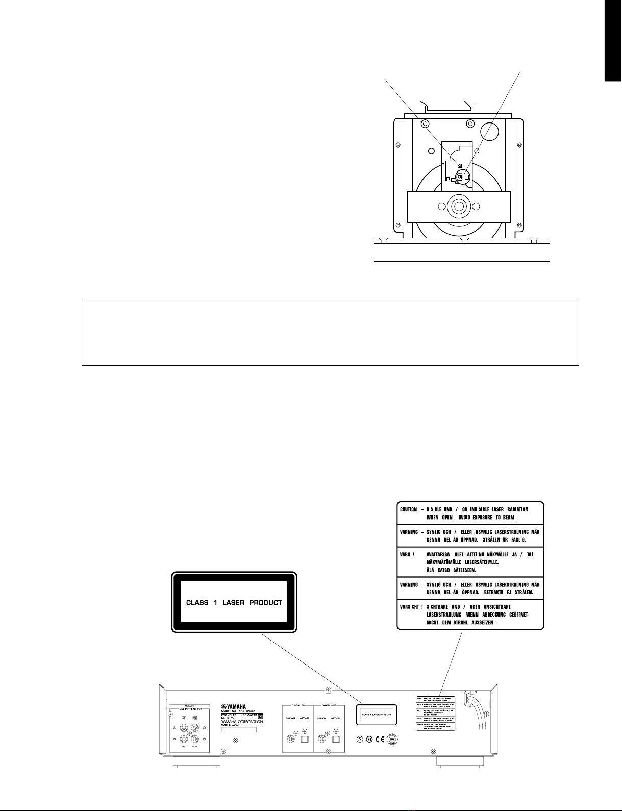
WARNING: Laser Safety
This product contains a laser beam component. This component may emit invisible, as well as visible radiation,
which may cause eye damage. To protect your eyes and skin from laser radiation, the following precautions must
be used during servicing of the unit.
1) When testing and/or repairing any component within the product, keep your eyes and skin more than 30 cm away from
the laser pick-up unit at all times. Do not stare the laser beam at any time.
2) Do not attempt readjustment, disassemble or repair of the laser pick-up, unless noted elsewhere in this manual.
3) CAUTION : Use of controls, adjustments or preformance of procedures other than those specified herein may result in
hazardous radiation exposure.
1. Critical Components Information
Components having special characteristics are marked Z
and must be replaced with parts having specifications equal
to those originally installed.
2. Leakage Current Measurement (For 120V Models Only)
When service has been completed, it is imperative to verify
that all exposed conductive surfaces are properly insulated
from supply circuits.
●Meter impedance should be equivalent to 1500 ohm shunted
by 0.15µF.
●Leakage current must not exceed 0.5mA.
■ TO SERVICE PERSONNEL
WARNING: CHEMICAL CONTENT NOTICE!
The solder used in the production of this product contains LEAD. In addition, other electrical/electronic and/or
plastic (where applicable) components may also contain traces of chemicals found by the California Health and
Welfare Agency (and possibly other entities) to cause cancer and/or birth defects or other reproductive harm.
DO NOT PLACE SOLDER, ELECTRICAL/ELECTRONIC OR PLASTIC COMPONENTS IN YOUR MOUTH FOR
ANY REASON WHATSOEVER!
Avoid prolonged, unprotected contact between solder and your skin! When soldering, do not inhale solder fumes
or expose eyes to solder/flux vapor!
If you come in contact with solder or components located inside the enclosure of this product, wash your hands
before handling food.
●Be sure to test for leakage with the AC plug in both
polarities.
Laser Emitting conditions:
1) When the Top Cover is removed, and POWER SW is turned to the "ON" position, the laser component will emit a beam
for several seconds to detect if a disc is present. During this time (5-10 sec.) the laser may radiate through the lens of
the laser pick-up unit. Do not attempt any servicing during this period !
If no disc is detected, the laser will stop emitting the beam. When a disc is set, you will not be exposed to any laser
emissions.
2) The laser power level can be adjusted with VR on pick-up PWB, however, this level has been set by the factory prior to
shipping from the factory. Do not adjust this laser level control unless instruuction is provided elsewhere in this manual.
Adjustment of this control can increase the laser emission level from the device.

CDR-S1000
CDR-S1000
2
Laser Diode Properties
Material : GaAlAs
Wavelength : 783 –789 nm
Emission duration : Continuous
Laser output : Max. 44.6µW*
ANSI Class : Class 1
* This output is the value measured at a distance of about
200 mm from the objective lens surface on the Optical Pick-
up Block.
A, B, G models
B, G models
VARO! : AVATTAESSA JA SUOJALUKITUS OHITETTAESSA OLET ALTTIINA NÄKYMÄTTÖMÄLLE
LASER-SÄTEILYLLE. ÄLÄ KATSO SÄTEESEEN.
VARNING! : OSYNLIG LASERSTRÅLNING NÄR DENNA DEL ÄR ÖPPNAD OCH SPÄRREN ÄR URKOPPLAD.
BETRAKTA EJ STRÅLEN.
Variable resistor
(Do not turn) Optical pick-up

CDR-S1000
CDR-S1000
■REAR PANELS
3
▼ U, C models
▼ A model
▼ B, G models

CDR-S1000
CDR-S1000
● DIMENSION
Unit : mm (inch)
■SPECIFICATIONS
GENERAL
Model Compact disc recorder
Application discs CDs, CD-Rs for AUDIO,
CD-RWs for AUDIO
Power Requirements
U, C models 120V AC 60Hz
B, G models 230V AC 50Hz
A model 240V AC 50Hz
Power Consumption 35W
Dimensions (W x H x D) 435 x 108 x 400mm
(17-1/8" x 4-1/4" x 15-3/4")
Weight 6.3kg (13 lbs 14 oz)
Operating Temperature Range +5˚C to +35˚C
Panel Color Black
AUDIO PERFORMANCE
Output Level
1kHz, 0dB 2.0 ±0.5Vrms
Frequency Response (EIAJ)
5Hz —20kHz ±0.5dB
Signal to Nosie Ratio (EIAJ)
Playback 107dB
Recording 90dB
Dynamic Range (EIAJ)
Playback 100dB
Recording 94dB
Total Harmonic Distortion (1kHz)
Playback 0.004%
Recording 0.008%
435 (17-1/8")
17
(11/16") 91
(3—9/16")
108
(4—1/4")
12
(1/2") 7
(1/4")
381 (15")
400 (15—3/4")
4
*Specifications are subject to change without notice.
U ...................U. S. A. model
C ................Canadian model
A .............. Australian model
B .................... British model
G ............... European model
INPUT/OUTPUT
Line Output
Output Level 2.0 Vrms
Output Impedance 990Ω
Line Input
Input Sensitivity 500m Vrms
Input Impedance 24kΩ(REC LEVEL Max.)
Digital Output
Coaxial Output Level 0.5Vp-p (75Ω)
Optical Output Level -20 dBm
Sampling Frequency 44.1kHz
Digital Input
Coaxial Input Level 0.5Vp-p (75Ω)
Optical Input Level -20 dBm
Input Gain ±12dB, with Digital Volume
±0dB, without Digital Volume
Sampling Frequency
Tolerance 32kHz to 48kHz, with SRC
44.1kHz ±100ppm, without SRC
(CD DIRECT mode)
Headphone Output
Output Level 300m Vrms (-20dB, 150Ωload)
(PHONES LEVEL Max.)

CDR-S1000
CDR-S1000
■INTERNAL VIEW
■DISASSEMBLY PROCEDURES (Remove parts in disassembly order as numbered.)
t!1
qw
y iu o !0
r
e
qANALOG P.C.B. (3)
wMAIN P.C.B. (1)
eCDR MECHANISM UNIT
rANALOG P.C.B. (1)
tPANEL P.C.B. (5)
yANALOG P.C.B. (2)
uPANEL P.C.B. (1)
iMAIN P.C.B. (2)
oPANEL P.C.B. (2)
!0 PANEL P.C.B. (3)
!1 PANEL P.C.B. (4)
CDR MECHANICAL UNIT REPLACEMENT
•When sending back the defective CDR mechanical unit for repair, send the whole unit.
•The CDR mechanical unit must be replaced as a unit. None of its components can be supplied separately.
•When sending back the defective CDR mechanical unit for repair, attach the disc which was used when the error
occurred as necessary. However, Yamaha shall not be liable even if the data in the disc has become unreadable while
the unit is being serviced/repaired.
Preparation before Replacement
a. When replacing the CDR mechanical unit, write down the following items.
•Serial No. of the product and the symptom in detail
•Mechanical serial No. / mechanical shipping serial No. of CDR mechanical unit
b. Prepare a lens cover (P/No. V4870500) to use when transporting the CDR mechanical unit.
Mechanical serial No. Shipping serial No.
Lens cover
5

CDR-S1000
CDR-S1000
6
Fig. 3
Fig. 1
r
e
q
q
CDR Mechanical Unit
w
t
t
1. CDR Mechanical Unit Removal
a. Turn off the power and disconnect the power plug from
the service outlet.
CAUTION : Never disconnect any cable, remove any
screw or other part while the power switch is on.
b. Remove 4 screws marked qand 1 screw marked w,
and the Top Cover can be removed. (Fig. 1)
c. Disconnect the power cable / IDE cable / word clock
cable from the CDR mechanical unit. (Fig. 2)
d. Remove 2 hexagonal cap nuts marked e. (Fig. 1)
e. Remove 4 screws marked r, and take out the CDR
mechanical unit. (Fig. 1)
f. Remove the Lid.
g. Remove 4 screws marked t, and the Frame/CDR can
be removed. (Fig. 3)
Top Cover Word Clock Cable
r
IDE Cable
Power Cable
CDR Mechanical Unit
CDR Mechanical Unit
Lid
Fig. 2
Frame/CDR
2. Transportation of CDR Mechanical Unit
a. When transporting the CDR mechanical unit, be sure to install the lens cover to it and put it in the anti-static bag before
packaging it.
IDE cable
a. Do not remove the cable from the female connector by
pulling on the cable.
b. Remove the connector from the female connector by in-
serting the minus driver into the insertion place and hook-
ing the female connector as per fig. A.
Fig. A
A insertion place

CDR-S1000
CDR-S1000
7
3. CDR Mechanical Unit Installation
a. Before installing the CDR mechanical unit, check that
the jumper pin on its rear panel is inserted in the MAS-
TER jack.
b. Install the components of the CDR mechanical unit cor-
rectly in the reverse order of the removal.
c. Use special care for the power cable of the CDR me-
chanical unit. If it is connected in reverse, the mechani-
cal unit will be damaged and fail to operate.
The end of the power cable with a red line is the No.1
pin side (+12V). Connect it to No.1 pin of the DC power
input connector.
d. The No.1 pin side of the IDE cable of the CDR mechani-
cal unit can be identified by a red line. Connect it to
No.1 pin of the IDE interface connector.
4. Operation Check after Installation
1) Checking after turning on the power
When the power is supplied, the CDR mechanical unit
executes self-diagnosis automatically.
If an error is detected in the initial self-diagnosis, LED
segments (LED601: ON/DISC, LED602: Read/Write) on
the front panel of the mechanical unit light up (in or-
ange) simultaneously and remain on.
If a malfunction has occurred, power on fails. (IDE com-
mand error)
2) Checking when malfunction has occurred
a. Check each cable for correct connection.
b. Check the power supply voltages. (Measure voltage at
the power connector of the mechanical unit.)
c. Check to ensure that the jumper pin on the rear panel is
inserted in the MASTER jack.
CDR mechanical unit
Usually called CDR/RW drive unit
Model name : ACRW100A
MASTER
Rear view (ACRW100A)
Front view (ACRW100A)
Tray Manual Eject Lever
LED Eject Switch
DC Input
IDE Interface Connector
Jumper Pin
Analog Audio Out
Word Clock Out
Frame Ground
WC
GND
Pin 40
Pin 1
Pin 2 qr

CDR-S1000
CDR-S1000
8
■SERVICE CHECK PROCEDURES
When the main unit fails to operate.
1. Check the power supply voltage of ANALOG P.C.B. (2).
Connector
W100
W201
CB601
Pin No.
1pin (+5V)
4pin (VP)
5pin (FL1)
6pin (FL2)
1pin (-VA)
3pin (+VA)
1pin (+12V)
4pin (+5V)
Specified voltage
5.0 ±0.25V
-27.0 ±1.5V
4.4 ±0.4Vrms
4.4 ±0.4Vrms
-9.5 ±0.8V
7.3 ±0.6V
12.0 ±0.6V
5.0 ±0.25V
Remarks
+5V power supply (Main P.C.B.)
-27V power supply (FL display)
+4V(AC) power supply (FL display)
-VA power supply (Analog P.C.B.)
+VA power supply (Analog P.C.B.)
+12V power supply (CDR drive)
+5V power supply (CDR drive)
2. Turn off the power to check the condition of the CDR drive section.
3. Disconnect the IDE cable.
4. Turn on the power and check the CDR drive section for proper operation.
(Check the condition of the CDR drive.)
The CDR drive should operate by itself.
(Focusing, disc motor revolution)
Operation failure means defective CDR drive.
5. Turn on the power again and check the CPU and FL display for proper operation.
Does the FL display light up after a few seconds?
Is the FL driver accessed?
(FL DATA, FL SCK, FLN CS)
6. Turn off the power and connect the IDE cable.
7. Start the TEST program and check the condition of the main P.C.B.(by using the self-
diagnosis function).
When skipping occurs from time to time, playback/recording is disabled.
1. Using a standard disc (TDK CD-RXA74 or TDK CD-RWXA74), check if recording and playback are executable.
CAUTION: How to handle discs
•Handle the disc with special care not to scratch it or make it dirty. Also do not expose it to ultra-violet rays when keeping it in
storage. (Greater care should be used than when handling a CD disc.)
•CD-RW74 can be used repeatedly but use a number of 20 times as a rough standard for the limit.
•If the CD-R is a self-record/playback type, it can be reused (for additional recording) unless it is finalized.
(Nothing can be recorded additionally if finalized.)
The CD-R disc which has not been finalized cannot be played back on a general type CD player..
•To play back the CD-RW, an applicable type CD player must be used.

CDR-S1000
CDR-S1000
9
Check the power
supply
NG
OK
Turn off the power to the drive section
to check its condition.
Disconnect the IDE cable.
Turn on the power and
check the operation.
NO
YES
If the drive starts operating by itself,
focusing functions properly and the
disc motor runs,
the drive section is in good condition.
Check the condition of the main P.C.B.
Both main P.C.B and CPU
are in good condition.
After some time
Does the display light up?
YES
YES
Driver IC, FL display failure
NO
NO
*1: FL_DATA, FL_SCK, FL_N_CS
Is the FL driver
accessed?
*1
CPU or connection may be defective.
Check the fault in the power
supply section.
If operation fails,
the drive section is defective.
SERVICE CHECK FLOW CHART

CDR-S1000
CDR-S1000
10
CB7
D3
■TEST PROGRAM
Starting the test program
Short the connector CB7 (2P).
+
POWER ON
Main memory check
Check the external memory (IC7).
OK
DSP3 register check
Check the DSP3 (IC205).
"DSP Reg" on the FL display
OK
"DSP Reg End" on the FL display
ACDR register check
Check the ACDR (IC4).
"ACDR Reg" on the FL display
OK
"ACDR Reg End" on the FL display
EEPROM check
Check the EEPROM (IC6).
"EROM Mem" on the FL display
OK
"EROM Mem End" on the FL display
End of the test program
AUDIO measurement mode is started.
"AMT mode" on the FL display
D3 (red) LED flashes at a high speed
NG
"DSP Reg Err" on the FL display
"ACDR Reg Err" on the FL display
"EROM Mem Err" on the FL display
When the test program is started, the memory and regis-
ter are checked automatically. If nothing is found faulty,
the AUDIO measurement mode is set.
NG
NG
NG
When canceling the test program or theAUDIO mea-
surement mode, turn off the power and correct short
circuit of the connector CB7 (2P).

CDR-S1000
CDR-S1000
11
INSPECTION SPECIFICATIONS
Step
1
2
Item
Display
SRC
Check method and standard
1. Check that all FL display units light up and go
off properly by pressing the DISPLAY key.
2. Cancel the all on or off state of display units by
pressing the ERASE key.
1. Set the INPUT selector to the OPTICAL posi-
tion.
2. Set the CD DIRECT key to the ON position.
3. Apply a 1kHz, -20dB digital signal to DIGITAL
IN (OPTICAL).
4. Check that the digital output level at DIGITAL
OUT (OPTICAL) is -20 ±2dB.
5. Set the CD DIRECT key to the OFF position.
6. Set the REC LEVEL control knob to the maxi-
mum position.
7. Check that the digital output level of at DIGI-
TAL OUT (OPTICAL) is -8 ±2dB.
8. Return the REC LEVEL control knob close to
the center position and check that the digital
output level at DIGITAL OUT (OPTICAL) can
be set to -20dB.
Input signal
DIGITAL IN
(OPTICAL)
1kHz, -20dB
Disc
No disc
No disc
Mode
Audio measurement mode
(ATM mode)
Audio measurement mode
(ATM mode)
Instruments Required for Inspection
•CD test disc (YEDS-18: TX911730) •CD-RW disc (TDK CD-RW AUDIO 74min [XA74])
•CD player with digital output (optical/coaxial) function (used as a digital signal generator)
•AV amplifier with digital input (optical/coaxial) function (used as a D/A converter)
•Signal generator (for analog signals) •Oscilloscope •Level meter
•Distortion meter
DIGITAL OUT
(OPTICAL)
CDR-S1000
CD player
DIGITAL IN
(OPTICAL) DIGITAL OUT
(OPTICAL)
AV amplifier
Oscilloscope
Level meter
DIGITAL IN
(OPTICAL)
AUDIO measurement function of the main unit panel
INPUT selector (at CD STOP)
•Selects the input signal.
•The selected input signal passes through DSP3 and is output to LINE
OUT (Analog) and DIGITAL OUT (Digital).Also, the level meter read-
ing is displayed in response to the input signal.
•In case of the digital signal, the sampling frequency is read from the
channel status and displayed as 32, 44.1 or 48 (kHz).
•When the subcode Q data is included in the digital signal, a part of
the subcode Q data appears on the FL display.
CD DIRECT key (at CD STOP)
•Selectsthedigital input signal passage, whether through SRC (Sample
Rate Converter) or direct. CD DIRECT LED lights up when the direct
signal passage is selected but this does not apply when the sampling
frequency is other than 44.1kHz ±200ppm.
REC LEVEL control knob
•When the digital input is selected, SRC is activated as the digital
volume controller.
If CD DIRECT is selected, however, the digital volume is set to through
(0dB) state.
•When the analog input is selected, this control knob functions as the
analog volume control.
DISPLAY key
Turns on and off all the display units.
To cancel the all on or off state of display units, press the ERASE key
and the original display state will be restored.
ERASE key
Cancels the all on or off state of display units.
PRE OUT
YEDS-18
Track 15 (1kHz, -20dB)
The output level of the digital signal (optical/coaxial) should be
checked by using the relative value of the analog demodulated
signal.

CDR-S1000
CDR-S1000
12
Step
3
Item
A/D converter
Check method and standard
1. Set the INPUT selector to the ANALOG posi-
tion.
2. Apply a 1kHz, 500mVrms analog signal to the
LINE IN (ANALOG).
3. Demodulate the digital signal of DIGITALOUT
(COAXIAL) to analog.
4. Adjusting the REC LEVEL control knob, check
that the demodulated signal level can be set
to 1Vrms. (The level meter should indicate -
6dB on display.)
5. At this time, check that the REC LEVEL con-
trol knob is close to the 12 o’clock position.
6. Check that the distortion factor is 0.03% or less.
7. Check that the S/N is 80dB or more. (Input
shorted, REC LEVEL max.)
8. Check that the frequency response (at 20Hz
and 20kHz) is 0 ±1.5dB.
Input signal
LINE IN (ANALOG)
1kHz, 20Hz, 20kHz
500mVrms
Disc
No disc
Mode
Audio measurement mode
(ATM mode)
CD player
Signal genarator
LINE IN
(ANALOG) DIGITAL OUT
(COAXIAL)
AV amplifier
Oscilloscope
Level meter
Distortion meter
DIGITAL IN
(COAXIAL)
Step
4
Item
D/A converter
Check method and standard
1. Cancel the audio measurement mode.
2. Turn on the power. (In normal mode)
3. Load the CD test disc (YEDS-18: TX911730).
4. Play track 2 (1kHz, 0dB).
5. Check that the output level of LINE OUT (ANA-
LOG) is 2 ±0.5Vrms.
6. Check that the distortion factor (1kHz) is 0.01%
or less.
7. Play tracks 3 (20Hz) and 6 (20kHz) and check
that the frequency response is 0 ±1.5dB.
8. Play track 7 and check that S/N is 100dB or
more.
Input signal Disc
YEDS-18
Mode
Normal mode
CDR-S1000
LINE OUT
(ANALOG)
Oscilloscope
Level meter
Distortion meter
Level meter
500mVrms
YEDS-18
Track 2 (1kHz, 0dB)
Track 3 (20Hz, 0dB)
Track 6 (20kHz, 0dB)
Track 7
PRE OUT
1kHz/20Hz/20kHz

CDR-S1000
CDR-S1000
13
CDR-S1000
LINE OUT
(ANALOG) Oscilloscope
Level meter
Distortion meter
Signal genarator
LINE IN
(ANALOG)
Step
5
Item
Recording
Playback
Check method and standard
1. Load the CD-RW disc (XA74).
2. Set the INPUT selector to the ANALOG posi-
tion.
3. Apply a 1kHz, 370mVrms analog signal to the
LINE IN (ANALOG).
4. Set the REC LEVEL control knob to the maxi-
mum position.
5. Execute recording/playback and check that the
output level at LINE OUT (ANALOG) is 2.0 ±
0.5Vrms.
6. Check that the distortion factor (1kHz) is 0.1%
or less.
7. Apply a 20Hz, 20kHz signals, execute record-
ing/playback and check that the level difference
is within 0 ±1.5dB.
Input signal
LINE IN (ANALOG)
1kHz, 20Hz, 20kHz
370mVrms
Disc
XA74
Mode
Normal mode
370mVrms
Level meter
1kHz/20Hz/20kHz

CDR-S1000
CDR-S1000
14
■IC DATA
IC5 : HD64F3039F18
CPU
NO.
1
2
3
4
5
6
7
8
9
10
11
12
13
14
15
16
17
18
19
20
21
22
23
24
25
PORT
PB0
PB1
PB2
PB3
PB4
PB5
MD2
PB7
TXD0
RXD0
/IRQ4
VSS
D0
D1
D2
D3
D4
D5
D6
D7
VCC
A0
A1
A2
A3
Name
N_DEV_RST
MUTE
DIP0
LED0
FL_SCK
FL_DATA
MD2
FL_N_CS
TXD0
RXD0
N_IRQ4
VSS
D0
D1
D2
D3
D4
D5
D6
D7
VCC
A0
A1
A2
A3
I/O
O
O
I
O
O
O
I
O
O
I
I
I/O
I/O
I/O
I/O
I/O
I/O
I/O
I/O
O
O
O
O
Function
Resetting peripheral devices
Muting output
DIP SW data
Operation check LED
Clock for FL driver control
Data for FL driver control
Setting CPU operation mode
Chip select for FL driver control
SCI0 output
SCI0 input
External interrupt (Blank)
GND
Data bus
Data bus
Data bus
Data bus
Data bus
Data bus
Data bus
Data bus
+ 5V power
Address bus
Address bus
Address bus
Address bus
A17/P51
A16/P50
A15/P27
A14/P26
A13/P25
A12/P24
A11/P23
A10/P22
A9/P21
A8/P20
VSS
A7/P17
A6/P16
A5/P15
A4/P14
A3/P13
A2/P12
A1/P11
A0/P10
VCC
P71/AN1
P70/AN0
AVSS
RESO/FWE
P65/WR
P64/RD
P63/AS
VCC
XTAL
EXTAL
VSS
NMI
RES
STBY
Ø
MD1
MD0
P60/WAIT
P53/A19
P52/A18
TIOCA3/TP8/PB0
TIOCA3/TP9/PB1
TIOCA4/TP10/PB2
TIOCB4/TP11/PB3
TOCXA4/TP12/PB4
TOCXB4/TP13/PB5
MD2
ADTRG/TP15/PB7
TXD0/P90
RXD0/P92
IRQ4/SCK0/P94
VSS
D0/P30
D1/P31
D2/P32
D3/P33
D4/P34
D5/P35
D6/P36
D7/P37
P72/AN2
P73/AN3
P74/AN4
P75/AN5
P76/AN6
P77/AN7
AVCC
P80/IRQ0
P81/IRQ1
P91/TXD1
P93/RXD1
P95/SCK1/IRQ5
PA0/TP0/TCLKA
PA1/TP1/TCLKB
PA2/TP2/TIOCA0/TCLKC
PA3/TP3/TIOCB0/TCLKD
A23/PA4/TP4/TIOCA1
A22/PA5/TP5/TIOCB1
A21/PA6/TP6/TIOCA2
A20/PA7/TP7/TIOCB2
61
62
63
64
65
66
67
68
69
70
71
72
73
74
75
76
77
78
79
80
40
39
38
37
36
35
34
33
32
31
30
29
28
27
26
25
24
23
22
21
1
2
3
4
5
6
7
8
9
10
11
12
13
14
15
16
17
18
19
20
60
59
58
57
56
55
54
53
52
51
50
49
48
47
46
45
44
43
42
41

CDR-S1000
CDR-S1000
15
NO.
26
27
28
29
30
31
32
33
34
35
36
37
38
39
40
41
42
43
44
45
46
47
48
49
50
51
52
53
54
55
56
57
58
59
60
61
62
63
64
65
66
67
68
69
70
71
72
73
74
75
76
77
78
79
80
IC5 : HD64F3039F18
CPU
PORT
A4
A5
A6
A7
VSS
A8
A9
A10
A11
A12
A13
A14
A15
A16
A17
A18
A19
/WAIT
MD
MD1
PHY
/STBY
/RES
NMI
VSS
EXTAL
XTAL
VCC
/AS
/RD
/WR
FWE
AVSS
AN0
AN1
AN2
AN3
AN4
AN5
AN6
AN7
AVCC
/IRQ0
/IRQ1
TXD1
RXD1
/IRQ5
PA0
PA1
PA2
PA3
PA4
PA5
PA6
PA7
Name
A4
A5
A6
A7
VSS
A8
A9
A10
A11
A12
A13
A14
A15
A16
A17
A18
A19
N_WAIT
MD
MD1
PHY
/STBY
/RES
NMI
VSS
EXTAL
XTAL
VCC
N_AS
N_RD
N_WR
FWE
AVSS
PUI_KEY0
PUI_KEY1
PUI_KEY2
PUI_KEY3
DIR0_VFL_S
PUI_KEY_VR
TEMP
SB_DIR0_O
AVCC
REMOCON
N_INT_CDR
TXD1
RXD1
N_INT_USB
SB_DATA
SB_SCK
SB_DIR0
SB_ADA
SB_DIT
SB_EEP
SB_EEP_DATA
CDR_FSCNT
I/O
O
O
O
O
O
O
O
O
O
O
O
O
O
O
O
O
I
I
I
O
I
I
I
I
O
O
O
O
I
I
I
I
I
I
I
I
I
I
I
O
I
I
O
O
O
O
O
O
I/O
I
Function
Address bus
Address bus
Address bus
Address bus
GND
Address bus
Address bus
Address bus
Address bus
Address bus
Address bus
Address bus
Address bus
Address bus
Address bus
Address bus
Address bus
WAIT input
Setting CPU operation mode
CPU operation clock output
Stand-by input
Resetting input
NMI input
GND
Terminal for crystal oscillator
+ 5V power
Address strobe
READ strobe
WRITE strobe
Flash write enable
GND for A/D
Key input
Key input
Key input
Key input
Detecting digital input validity flag
Panel volume data
Measuring temperature by using thermistor
Reading data of DIR for SPDIF
+ 5V power for A/D
External interrupt (Remote control)
External interrupt (ACDR)
SCI1 output
SCI1 input
External interrupt (USB)
Three-wire serial data
Three-wire serial clock
Chip select of DIR for SPDIF
Chip select for AD/DA
Chip select for DIT (Unused)
EEPROM clock
EEPROM data
Counting frequency of SPDIF input

CDR-S1000
CDR-S1000
16
Pin
No.
1
2
3
4
5
6
7
8
9
10
11
12
13
14
15
16
17
18
19
20
21
22
23
24
25
Pin
No.
26
27
28
29
30
31
32
33
34
35
36
37
38
39
40
41
42
43
44
Pin
Name
DAUX
HDLT
DOUT
VFL
OPT
SYNC
MCC
WC
MCB
MCA
SKSY
XI
XO
P256
LOCK
Vss
TC
DIM1
DIM0
DOM1
DOM0
KM1
RSTN
Vdda
CTLN
Function
Auxiliary input for audio data
Asynchronous buffer operation flag
Audio data output
Parity flag output
Fs x 1 Synchronous output signal for DAC
Fs x 1 Synchronous output signal for DSP
Fs x 64Bit clock output
Fs x 1Word clock output
Fs x 128Bit clock output
Fs x 256Bit clock output
Clock synchronization control input
Crystal oscillator connection or external
clock input
Crystal oscillator connection
VCO oscillating clock connection
PLL lock flag
Logic section power (GND)
PLL time constant switching output
Data input mode selection
Data output mode selection
Clock mode switching input 1
System reset input
VCO section power (+5V)
VCO control input N
Pin
Name
PCO
(NC)
CTLP
Vssa
TSTN
KM2
KM0
FS1
FS0
CSM
EXTW
DDIN
LR
Vdd
ERR
EMP
CD0
CCK
CLD
I/O
I
O
O
O
O
O
O
O
O
O
I
I
O
O
O
O
I
I
I
I
I
I
I
I/O
O
I
I
I
I
O
O
I
I
I
O
O
O
O
I
I
Function
PLL phase comparison output
VCO control input P
VCO section power (GND)
Test terminal. Open for normal use
Clock mode switching input 2
Clock mode switching input 0
Channel status sampling frequency display
output 1
Channel status sampling frequency display
output 0
Channel status output method selection
External synchronous auxiliary input word
clock
EIAJ (AES/EBU) data input
PLL word clock output
Logic section power (+5V)
Data error flag output
Channel status emphasis control code out-
put
3-wire type microcomputer interface data
output
3-wire type microcomputer interface clock
input
3-wire type microcomputer interface load
input
DAUX
HDLT
DOUT
VFL
OPT
SYNC
MCC
WC
MCB
MCA
SKSY
XI
XO
P256
LOCKN
VSS
TC
DIM1
DIM0
DOM1
DOM0
KM1
CLD
CCK
CDO
EMP
ERR
VDD
LR
DDIN
EXTW
CSM
FS0
FS1
KM0
KM2
TSTN
VSSa
CTLP
(N.C.)
PCO
CTLN
VDDa
RSIN
1
2
3
4
5
6
7
8
9
10
11
12
13
14
15
16
17
18
19
20
21
22 34
35
36
37
38
39
40
41
42
43
44
23
24
25
26
27
28
29
30
31
32
33
IC8, 206 : YM3436DK
DIR (Digital Format Interface Receiver)
EIAJ (AES/EBU)
DIGITAL AUDIO
INTERFACE
DECODER
DATA CLOCK
CONTROLLER
SYSTEM
CLOCK
TIMING
GENERATOR
SEL
SERIAL INTERFACE
BUFFER
32 29 15 14 13 12 31 22 11 23
10
9
8
7
6
5
3
2
424344 16 39 3019181
4
20
21
37
40
35
41
33
34
P/S
S/P
24 26 28 25 17
PLL
38
MCA
KMO
CLD
CCK
CDO
DAUX
DIM1
DIM0
HDLT
VSS
VDD
TSTN
VSSA
VDDA
PCO
CTLP
CTLN
TC
LR
LOCKN
P256
X0
X1
KM2
KM1
SKSY
RS IN
MCB
WC
MCC
SYNC
OPT
VFL
D OUT
D DIN
ERR
CSM
36
EXTW
EMP
FS1
FS0
DOM1
DOM0

CDR-S1000
CDR-S1000
17
IC4 : FHIB31-70A
ACDR
DD15
120 DD14
11 DD13
118 DD12
117 DD11
116 DD10
11 DD9
114 DD8
113 VSS112 DD7
111 DD6
110 DD5
109 DD4
108
59 VDD
58 PO6
57
56
55
54 PI5
53 PI652 PI751 PI8
50 /DS
49 /CS
48
47 /RD
46 /WR
45 /IRQ
44 FSCNT
43 /IC
42 VSS
41
BCKI
78 DINS
77
ICLK
80 LRCI
79
76
75
74 F641
73 WC1
72
71 VSS
70
69
68
67
66
65
64
63
62
61
60
13
RD5 DD3
107
14
RD4 DD2
106
15
RD3 DD1
105
16
RD2 DD0104
17
RD1 103
18
RD0 VSS
102
19
VDD VDD
101
20
VSS DIFI
100
99
98
97
96
95
94
93
92
91
90
89
88
87
86
85
84
83
82
81
21
12
RD6 11
RD7 10
VSS 9
RD8 8
RD9 7
RD10 6
RD11 5
RD12 4
3
2
RD15 1
34
35
36
37
38
39
40
33
32
31
30
29
28
27
26
25
24
23
22
VSS
SPDI
DIF
SPD
WCIN
PO0
PO1
PO2
PO3
PI0
PI1
PI2
PI3
PI4
D6 EXTW2
D5
D4 F642
D3 WC2
D2 F2562
D1 VSS
D0
D7
A0
A1
A2
A3
A4
A5
A6
A7
160
/OE 159
/W 158
RA0 157
RA1 156
RA2 155
RA3 154
RA4 153
RA5 152
RA6 151
RA7 150
VSS 149
148
RA9 147
146
145
144
143
142
141
140
VSS 139
VDD 138
CK33O 137
136
DASP 135
134
133
HA2 132
HA1 131
HA0 130
CSEL 129
128
127
126
125
124
VSS 123
122
121
RD13
RD14
SDIA
SDIB
SDOA
SDOB
DOUTS
EXTW1
SYNC1
F2561
OCLK
LRCO
BCKO
WC3
DDO
MUTEA
MUTEB
DIN
VSS
PO4
PO5
PO7
PO8
PO9
/WAIT
/HRST
SYNC2
IOCS16
HINTRQ6
HDMARQ
IORDY
PDIAG
/HIOW
/HIOR
/HDACK
/HCS0
/HCS1
CK33I
RA16
RA8
RA10
RA11
RA12
RA13
RA14
RA15
NO.
1
2
3
4
5
6
7
8
9
10
11
12
13
14
15
16
17
18
19
20
21
22
23
24
PORT
VSS
RD15
RD14
RD13
RD12
RD11
RD10
RD9
RD8
VSS
RD7
RD6
RD5
RD4
RD3
RD2
RD1
RD0
VDD
VSS
SDIA
SDIB
SDOA
SDOB
Name
VSS
CDR_RD15
CDR_RD14
CDR_RD13
CDR_RD12
CDR_RD11
CDR_RD10
CDR_RD9
CDR_RD8
VSS
CDR_RD7
CDR_RD6
CDR_RD5
CDR_RD4
CDR_RD3
CDR_RD2
CDR_RD1
CDR_RD0
VDD
VSS
CDR_SDIA
DA_DATA
CDR_SDOA
CDR_SDOB
I/O
I/O
I/O
I/O
I/O
I/O
I/O
I/O
I/O
I/O
I/O
I/O
I/O
I/O
I/O
I/O
I/O
I
I
O
O
Function
GND
External RAM data bus
GND
External RAM data bus
Power supply
GND
Serial audio data input
Serial audio data output
DC
T
T
T
T
T
T
T
T
T
T
T
T
T
T
T
T
T
T
C
C

CDR-S1000
CDR-S1000
18
IC4 : FHIB31-70A
ACDR
NO.
25
26
27
28
29
30
31
32
33
34
35
36
37
38
39
40
41
42
43
44
45
46
47
48
49
50
51
52
53
54
55
56
57
58
59
60
61
62
63
64
65
66
67
68
69
70
71
72
73
74
75
76
77
78
79
PORT
A7
A6
A5
A4
A3
A2
A1
A0
D7
D6
D5
D4
D3
D2
D1
D0
VSS
/IC
FSCNT
/IRQ
/WR
/RD
/WAIT
/CS
/DS
PI8
PI7
PI6
PI5
PO9
PO8
PO7
PO6
PO5
PO4
VDD
VSS
DIN
MUTEB
MUTEA
DD0
WC3
BCKO
LRCO
OCLK
VSS
F2561
WC1
F641
SYNC1
EXTW1
DOUTS
DINS
BCKI
LRCI
Name
A7
A6
A5
A4
A3
A2
A1
A0
D7
D6
D5
D4
D3
D2
D1
D0
VSS
N_DEV_RST
CDR_FSCNT
N_INT_CDR
N_WR
N_RD
N_CDR_WAIT
N_CDR
N_DS
JG_PIN1
JG_PIN0
DIP3
DIP2
LED2
LED1
DIT_CNTR
SRC_SLW
VDD
VSS
CDR_DIN
MUTEB
MUTEA
CDR_SPD
DIR0_FS
VSS
DIR1_256FS1
DIR1_FS
DIR1_64FS
DIR1_SYNC
EXTW1
DOUTS
DINS
I/O
I
I
I
I
I
I
I
I
I/O
I/O
I/O
I/O
I/O
I/O
I/O
I/O
I
O
O
I
I
O
I
I
I
I
I
I
O
O
O
O
O
O
I+
I
I
O
I$
O$T
O$T
O$
I$
I$
I$
I
O$
O
I
O$T
O$T
Function
CPU interface address bus
CPU interface data bus
GND
Initial clear
Fs count signal output
CPU interface interrupt request
CPU interface write strobe
CPU interface read strobe
CPU interface wait
CPU interface chip select
CPU interface data strobe
Extended input port for H8
Extended output port for H8 (N.C.)
Extended output port for H8
Power supply
GND
Digital audio data input
Digital audio interface output mute
Digital audio data output
Word clock input
Bit clock output (N.C.)
LR clock output (N.C.)
Clock output (N.C.)
GND
Clock input (256fs)
Word clock input
Clock input (64fs)
Synchronous signal input
Word clock output (fs)
Serial audio data output
Serial audio data input
Bit clock output (N.C.)
LR clock output (N.C.)
DC
T
T
T
T
T
T
T
T
T
T
T
T
T
T
T
T
T
C
C
T
T
C
T
T
T
T
T
T
C
C
C
C
C
C
T
T
T
C
T
C
C
C
T
T
T
T
C
C
T
C
C

CDR-S1000
CDR-S1000
19
IC4 : FHIB31-70A
ACDR
NO.
80
81
82
83
84
85
86
87
88
89
90
91
92
93
94
95
96
97
98
99
100
101
102
103
104
105
106
107
108
119
110
111
112
113
114
115
116
117
118
119
120
121
122
123
124
125
126
127
128
129
130
131
132
133
134
PORT
ICLK
VSS
F2562
WC2
F642
SYNC2
EXTW2
PI4
PI3
PI2
PI1
PI0
PO3
PO2
PO1
PO0
WCIN
SPD
DIF
SPDI
DIFI
VDD
VSS
/HRST
DD0
DD1
DD2
DD3
DD4
DD5
DD6
DD7
VSS
DD8
DD9
DD10
DD11
DD12
DD13
DD14
DD15
IOCS16
HINTRQ
HOMARQ
VSS
IORDY
PDIAG
/HIOW
/HIOR
/HDACK
CSEL
HA0
HA1
HA2
/HCS0
Name
VSS
DIR1_256FS1
DIR1_FS
DIR1_64FS
DIR1_SYNC
DIP1
DIR1_N_LOCK
DIR1_ERR
DIR0_N_LOCK
DIR0_ERR
JG_POUT2
JG_POUT1
JG_POUT0
OPT_IN
WCIN
SPD
DIT_OUT
DIFI
VDD
VSS
IDE_N_RST
IDE_D0
IDE_D1
IDE_D2
IDE_D3
IDE_D4
IDE_D5
IDE_D6
IDE_D7
VSS
IDE_D8
IDE_D9
IDE_D10
IDE_D11
IDE_D12
IDE_D13
IDE_D14
IDE_D15
IDE_N_IOCS16
IDE_INTRQ
IDE_DMARQ
VSS
IDE_IORDY
IDE_N_PDIAG
IDE_N_IOW
IDE_N_IOR
IDE_N_DMACK
IDE_CSEL
IDE_A0
IDE_A1
IDE_A2
IDE_N_CS0
I/O
O$
I$
I$
I$
I
O$
I
I
I
I
I
O
O
O
O
I$
O
O
I
I
OT
I/O
I/O
I/O
I/O
I/O
I/O
I/O
I/O
I/O
I/O
I/O
I/O
I/O
I/O
I/O
I/O
I
I
I
I
OD
OT
OT
OT
O
OT
OT
OT
OT
Function
Clock output (N.C.)
GND
Clock input (256fs)
Word clock input (fs)
Clock input (64fs)
Synchronous signal input
Word clock output (N.C.)
Extended input port for H8
Extended output port for H8
Word clock input
Digital audio interface output
Digital audio interface output (N.C.)
Digital audio interface input
Power supply
GND
EDE interface reset
IDE interface data bus
GND
IDE interface data bus
IDE interface data bus width specify
IDE interface interrupt request
IDE interface DMA request
GND
IDE interface data ready
IDE interface connection diagnosis control
IDE interface DMA write strobe
IDE interface DMA read strobe
IDE interface DMA data acknowledge
IDE interface device select
IDE interface address
IDE interface chip select
DC
C
T
T
T
T
C
T
T
T
T
T
C
C
C
C
T
C
C
T
T
C
T
T
T
T
T
T
T
T
T
T
T
T
T
T
T
T
T
T
T
T
C
C
C
C
C
C
C
C
C
Other manuals for CDR-S1000
1
Table of contents
Other Yamaha Recording Equipment manuals

Yamaha
Yamaha E1005 User manual

Yamaha
Yamaha REV-5 User manual

Yamaha
Yamaha WX-11 User manual

Yamaha
Yamaha PM5D-RH User manual

Yamaha
Yamaha MCX-C15 - MusicCAST Network Audio Player User manual

Yamaha
Yamaha Midi XG MU90R User manual

Yamaha
Yamaha SPX90 User manual

Yamaha
Yamaha TG55 User manual

Yamaha
Yamaha EME-1 User manual

Yamaha
Yamaha TQ5 User manual

Yamaha
Yamaha NAI48-ES Setup guide

Yamaha
Yamaha MR816CSX User manual

Yamaha
Yamaha DP-U50 User manual

Yamaha
Yamaha REV7 User manual

Yamaha
Yamaha QX-5FD User manual

Yamaha
Yamaha MDR-10 User manual

Yamaha
Yamaha WX-11 User manual

Yamaha
Yamaha Audiogram 3 User manual

Yamaha
Yamaha MU15 User manual

Yamaha
Yamaha QX-3 User manual