Zoom G1 X Four User manual


- 2 -
Contents
Specifications…………………………………………………………………………………………3
Function Test …………………………………………………………………………………………4
Back Up User’s Data…………………………………………………………………………………9
Recovering the Factory Default …………………………………………………………………….11
Special function start up ……………………………………………………………………………12
Circuit Check Specifications ………………………………………………………………………15
PCB Parts Layout and Pattern ……………………………………………………………………16
Circuit Diagram …………………………………………………………………………………… 17
Exploded view………………………………………………………………………………………20
Parts List ……………………………………………………………………………………………22
Spare Parts Order List ………………………………………………………………………………28
Spare Parts Order Sheet ……………………………………………………………………………30
Supplement: Identification of main PCB ………………………………………………………………31
Supplement: The major difference between before No.022150 and after No.022151 …………………32

- 3 -
Specifications
Effect types 54
Effect modules max. 8 simultaneous modules
Patch memory User area: 10 patches x 4 banks = 40
Preset area: 10 patches x 4 banks = 40
Total 80 patches
Sampling frequency 96 kHz
A/D converter 24 bit, 128 times oversampling
D/A converter 24 bit, 128 times oversampling
Signal processing 32 bit
Frequency response 20 Hz – 40 kHz +1.0 dB – 4.0 dB (10kilohms load)
Display 2-digit 7-segment LED
Input Standard mono phone jack
Rated input level -20 dBm
Input impedance 470 kilohms
Output Standard stereo phone jack (doubles as line/headphone
jack)
Maximum output level Line +3 dBm (output load impedance of 10 kilohms or
more)
Phones 20mW + 20mW (into 32ohms load)
Power requirements
AC adapter 9 V DC, 300 mA (center minus plug) (ZOOM
AD-0006)
Batteries Four IEC R6 (size AA) batteries, approx.
12 hours continuous operation (alkaline batteries)
Dimensions 155 mm (D) x 234 mm (W) x 52 mm (H)
Weight 600 g (without batteries)
• 0 dBm = 0.775 Vrms
• Design and specifications subject to change without notice.

- 4 -
Function Test
Starting in “Test mode”
1) Start up the G1X in the following ways using the AC adaptor AD-0006.
a) Connect AC adaptor holding the [BANK UP・TAP] key (SW1) and [RHYTHM] key (SW2).
b) Connect AC adaptor when Ground and the test point TP1.
*When set 4 batteries, connect the plug into INPUT connector (J2)
2) All the LEDs of 7 segment LED will be lit.
1. Display (7 segment LED)
1) Make sure that all LEDs are lit brightly enough (indicate “8.8.”) after power on in “Test mode”.
2) Press any key and make sure that all LEDs will be turned off.
2. Module selector
1) Turn the Module selector (VR1) clockwise to “DECAY”.
2) Turn the Module selector (VR1) anticlockwise by one detent.
Make sure that the following indications appear on the 7 segment LED.
Module selector 7 segment LED
DECAY 15
REVERB 14
TIME 13
DELAY 12
RATE 11
MODULATION 10
ZNR/AMP 9
EQ_Hi 8
EQ_Mid 7
EQ_Lo 6
GAIN 5
DRIVE 4
COMP/EFX 3
PATCH LEVEL 2
RHYTHM 1
PLAY 0
3) Turn the Module selector (VR1) clockwise by one detent.
Make sure that the above values are indicated on the 7 segment LED depending on the
Module selector position.
Like figure 1 of the following page, make sure that replaced by right numerical value
at a click point and intermediate between click point.
In a range of the same click point, numerical value replaced is NG.

- 5 -
Figure 1.16 clicks value confirmation position
3. Knob
Turn the [VALUE] knob (SW6) and 7 segment LED indicates “00–FF”.
Make sure that indication smoothly changes in the range of “00-FF” and the value
changes 1 step by 1 detent.
4. Flash ROM
Press the [BANK UP・TAP] key (SW1).
Make sure that “ok” appears on the 7 segment LED.
If any error occurs, “nG” is indicated on the 7 segment LED.
5. Product number
1) Press the FOOT SWITCH [^] (SW5).
Make sure that “GP” is indicated on the 7 segment LED.
2) Press the FOOT SWITCH [^] (SW5) again.
i) Serial No. 000001 - 022150
Make sure that “87” or “11” are indicated on the 7 segment LED.
ii) Serial No. 022151 –
Make sure that “d2” is indicated on the 7 segment LED.
①
②
③
④
⑤
⑥
⑦
⑧
⑨⑩⑪
⑫
⑬
⑭
⑮
⑯
⑰
⑱
⑲
②④⑯⑱
※It is NG that a
value changes in a
click.
0
1
2
3
4
5
67 8
9
10
11
12
13
14
15
There is a change in
a click
(allowance)=
NG
It is OK to change with a
dark color.
It is OK to change with a
dark color.
①③⑤~⑮⑰⑲
※A value changes in
a range of arrow
Inspection judgment standard of 16 click setting.
0->1、2->1
13->14、15->14
Attention at the time
of setting
↓
allowance
It must
consciously setting
that center of
allowance.

- 6 -
6. PEDAL ASSIGN check
Press the PEDAL ASSIGN key, and make sure that the 7segment LED is displayed [SL].
And make sure that the PEDAL ASSIGN LED turns on in the order of “VOL ->WAH
-> DRY ->MOD ->DLY ->REV -> turns off”, whenever the key is pressed.
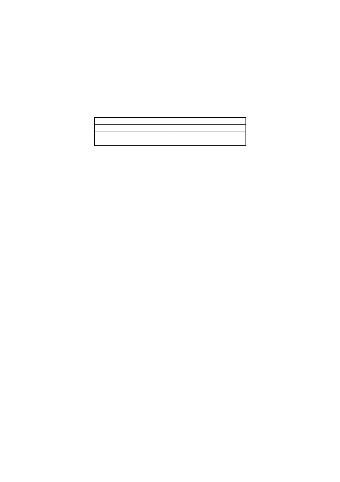
7. EX Pedal
The 7segment LED is displayed EX PEDAL’s AD value if the PEDAL is moved.
Make sure that this EX PEDAL’s AD value is the same as below table.
Expression pedal Values
MIN(raise) 09 - 29
MAX(down) 30 - 80
Pushed all the way [VOLUME] LED blinking
Make sure that difference between MIN and MAX is 20 or more in hex and this value doesn’t
decrease if EX PEDAL is pressed down.
Make sure that all PEDAL ASSIGN LEDs are blinking by pressing down the
EX PEDAL stronger.
8. Through sound
Input sine wave (440Hz, -20dBm) to the [INPUT] jack (J2) and monitor the output from
the [OUTPUT] jack (J4) with loudspeakers and oscilloscope.
Make sure that the sounds from both channel of [OUTPUT] jack (J4) are at the same
volume, without any noise and improper sound.
If “Mt” or “dL” is indicated on the 7 segment LED, press any key among [BANK UP
・TAP] key (SW1), [STORE] (SW3) and FOOT SWITCH [^] (SW5). Then make sure
that indication is changes to other.
9. SRAM (Delay sound)
1) Press [RHYTHM] (SW2) key and display indicates “dL”.
2) Input sine wave (440Hz, -20dBm) to the [INPUT] jack (J2) and monitor the output
from the [OUTPUT] jack (J4) with loudspeakers and oscilloscope.
Make sure that the normal signal is output from Rch and the delayed signal is output
from the Lch of [OUTPUT] jack (J4) when “dL” is constantly indicated.
10. DSP mute
1) Press FOOT SWITCH [v] (SW4) and display indicates “Mt”.
2) Input sine wave (440Hz, -20dBm) to the [INPUT] jack (J2) and monitor the output
from the [OUTPUT] jack (J4) with loudspeakers and oscilloscope.
Make sure that there is no output when “Mt” is constantly indicated.

- 7 -
11. Restoring Factory Defaults
1) Power on in normal mode.
If 7segment LED doesn't blink “AL", power on pressing the "STORE" key.
Note) If someone make the operation below, after that 7segment LED never show "AL"
2) Make sure that display blinks “AL”
3) Press [STORE] key (SW3) and display indicates “ok”.
4) The units automatically reboot in normal mode.
12. Sound check 1
1) Connect AC adaptor and the unit’s power on.
2) Make sure that display indicates [A0].
3) Press the FOOT SWITCH [^] (SW5) two times and make sure that display changes
to [A2].
4) Input sine wave (440Hz, -20dBm).
5) Monitor output sound by speaker or oscilloscope and make sure the points below.
Output sound is distorted.
Sound doesn’t include abnormal noise, and this sound isn’t abnormal sound.
6) Make sure that frequency of 1 Octave change by moving the EX-PEDAL.
13. Sound check 2
1) Press the FOOT SWITCH [v] (SW4) and make sure that display changes to [A1].
2) Input sine wave (440Hz, -20dBm)
3) Monitor output sound by speaker or oscilloscope and make sure the points below.
Output sound is modulated.
Sound doesn’t include abnormal noise, and this sound isn’t abnormal sound.
4) Add mechanical shock to the units a few times and make sure there are no any
problem like noise or sound stop.

- 8 -
14. Battery
1) Disconnect AC adaptor and set the power supply voltage to 6.0 V.
2) Make sure that “A0” is indicated on the 7 segment LED.
3) Set the power supply voltage to 3.7 V.
Make sure that the indication “bt” appears on the 7 segment LED.
4) Set the power supply voltage to 4.6 V.
Make sure that the 7 segment LED indication returns to the previous state.
15. Stability
Put the G1X on a surface plate, and push it diagonally.
Make sure that there is no remarkable space (less than ±0.3 mm is acceptable).

- 9 -
Back Up User’s Data
If necessary, back up the user’s effect patch data to avoid an accidental erasing.
Required
· User’s G1X as a transmitter (hereinafter referred to as “the transmitter”)
· Another G1X as a receiver (hereinafter referred to as “the receiver”)
· Jumper wires
1. Remove the bottom plate.
2. Connect “IN” terminal of the transmitter and “OUT” terminal of the receiver.
3. Connect “OUT” terminal of the transmitter and “IN” terminal of the receiver.
4. Connect their ground terminals on the top side of the main PCB, using jumper wires (See
below).
Transmitter Receiver
Main PCB top side Main PCB top side
5. Turn on the power of both transmitter and receiver while holding the [STORE] (SW3) and
the [BANK UP・TAP] (SW1) keys.
Make sure that the both 7segment LED lit "tr".

- 10 -
6. Press the [BANK UP・TAP] key (SW1) of the receiver, and make sure that the 7 segment
LED lit “rx”. The receiver is ready to receive the data.
7. Press the [Rhythm] key (SW2) of the transmitter and make sure that the 7 segment LED
lit “tx”. The indication flashes on and off at once. And the transmitter starts to send the
data. When sending and receiving finish successfully, and make sure that Transmitter
and Receiver’s both 7 segment LED are displayed same check-sum.
8. Turn the both transmitter and receiver off.
9. Take the wires away and attach the bottom plate.

- 11 -
Recovering the Factory Default
In the factory default condition, the patches of the user area (A0-d9) contain the same settings as the
patches of the preset area (00-39).
Even after overwriting the user patches, their original content can be restored in a single operation
(“All Initialize” function).
If necessary, back up the user’s patch data. Refer to page 9, 10 for details of the back up.
1. Turn the power on while holding the [STORE] key (SW3).
The indication “AL” appears on the display.
2. To carry out the All Initialize function, press the [STORE] key (SW3) once more.
All patch settings are returned to the factory default condition, and the unit switches to
play mode. To cancel All Initialize, press the[RHYTHM] key (SW2) instead of the [STORE] key
(SW3).

- 12 -
Special function start up
1. Special function and how to start up
There are some methods to start up the G1X for service.
All special functions start up the G1X in the following ways using the AC adaptor AD-0006 or
connecting the plug into INPUT connector (J2) when set the battery.
Turn on the G1X holding the key in the following table.
See the following table about Special function.
Function Keys held down
Test mode RHYTHM + BANK UP・TAP
16 click adjust STORE + RHYTHM
Back up user’s data STORE + BANK UP・TAP
ALL Initialization STORE
Pedal calibration PEDAL ASSIGN
Pre-select UP ([^])
Revision RHYTHM + DOWN ([v])
Version BANK UP・TAP + UP([^])
2.Details of special function
●Test mode
This startup is used for the function Test.
Refer to page 4.
●16 click adjust
Adjust the threshold of 16 click vol. (from 0 click to 15 click)
1) Start up holding the [STORE] key (SW3) and [RHYTHM] key (SW2).
Make sure “1” appears on the 7 segment LED.
2) Turn the Module selector (VR1) clockwise by one detent.
Press the [STORE] key (SW3). *Refer to the figure below.
Make sure “2” appears on the 7 segment LED.
3) Turn the Module selector (VR1) clockwise by one detent.
Press the [STORE] key (SW3).
Repeat this sequence to “DECAY”.
(When “PATCH LEVEL”, 7 segment LED is displayed “3”.
When “COMP/EFX”, 7 segment LED is displayed “4”.
.
.
.
When “REVERB”, press the [STORE] key (SW3), 7 segment LED is displayed “15”.)
Make sure “-14” appears on the 7 segment LED.
4) Turn the Module selector (VR1) anticlockwise by one detent.
Press the [STORE] key (SW3).
Make sure “-13” appears on the 7 segment LED.

- 13 -
5) Turn the Module selector (VR1) anticlockwise by one detent.
Press the [STORE] key (SW3).
Repeat this sequence to “PLAY”.
( When “TIME”, 7 segment LED is displayed “-12”.
When “DELAY”, 7 segment LED is displayed “-11”.
.
.
.
When “RHYTHM”, 7 segment LED is displayed “0”. )
Make sure “ok” appears on the 7 segment LED.
6) Make sure that the following indications appear on the 7 segment LED.
When the 7 segment LED is correctly displayed, Restart the G1X by press the [BANK
UP・TAP] key (SW1).
Module selector 7 segment LED
PLAY 0
RHYTHM 1
PATCH LEVEL 2
COMP/EFX 3
DRIVE 4
GAIN 5
EQ Lo 6
EQ Mid 7
EQ Hi 8
ZNR/AMP 9
MODULATION 10
RATE 11
DELAY 12
TIME 13
REVERB 14
DECAY 15
①
②
③
④
⑤
⑥
⑦
⑧
⑨⑩⑪
⑫
⑬
⑭
⑮
⑯
⑰
⑱
⑲
②④⑯⑱
※It is NG that a
value changes in a
click.
0
1
2
3
4
5
67 8
9
10
11
12
13
14
15
There is a change in
a click
(allowance)=
NG
It is OK to change with a
dark color.
It is OK to change with a
dark color.
①③⑤~⑮⑰⑲
※A value changes in
a range of arrow
Inspection judgment standard of 16 click setting.
0->1、2->1
13->14、15->14
Attention at the time
of setting
↓
allowance
It must
consciously setting
that center of
allowance.

- 14 -
●ALL Initialization
This startup recovers the factory default condition.
Refer to page 10.
●Pedal calibration
Used to readjust the expression pedal operation.
Refer to page 26 of the G1/G1X operation manual.
●Pre-select
See the Operation Manual.
●Back up user’s data
This startup is used for back up user’s data.
Refer to page 8.
●Version
The 7 segment LED is displayed system version of the G1.
* It is displayed in four digits.
1) Start up holding the [BANK UP・TAP] key (SW1) and
the FOOT SWITCH [^] (SW5).
Make sure “00” appears on the 7 segment LED.
2) Press the FOOT SWITCH [^](SW5) or [v] (SW4).
i) Serial No. 000001 - 022150
Make sure “10” appears on the 7 segment LED.
ii) Serial No. 022151 –
Make sure “12” appears on the 7 segment LED.
3) Restart the G1X by press the FOOT SWITCH [^] (SW5) or [v] (SW4) again.
●Revision
The 7 segment LED is displayed system revision of the G1.
* It is displayed in four digits.
1) Start up holding the [RHYTHM] key (SW2) and
the FOOT SWITCH [v] (SW4).
Make sure “00” appears on the 7 segment LED.
2) Press the FOOT SWITCH [^] (SW5) or [v] (SW4).
i) Serial No. 000001 - 022150
Make sure “46” appears on the 7 segment LED.
ii) Serial No. 022151 –
Make sure “48” appears on the 7 segment LED.
3) Restart the G1X by press the FOOT SWITCH [^] (SW5) or [v] (SW4) again.

Circuit Check Specifications
No. Items Ch Specifications Inputs Conditions/notes Displayand Indicator Keys pressed in "Test mode"
1 Current consumption 125mA±20mA Short Immediately after Test mode starts All LEDs are lit. All lit None (Start up)
2 Power supply voltage 3.3VA 3.3V±0.15V Short Immediately after Test mode starts All LEDs are lit. All lit None(Start up)
+3.3VD 3.3V±0.15V Short Immediately after Test mode starts All LEDs are lit. All lit None(Start up)
+1.26VD 1.25V±0.05V Short Immediately after Test mode starts All LEDs are lit. All lit None(Start up)
-5VA -4.75V±0.25V Short Immediately after Test mode starts All LEDs are lit. All lit None(Start up)
3 Output level ( L ) -22.5dBm±2dB 440Hz -20dBm Load=32 ohms / Output waveform is not clipped. All lit None(Start up)
(Load: 32 ohms) ( R ) -22.5dBm±2dB 440Hz -20dBm Load=32 ohms / Output waveform is not clipped. All lit None(Start up)
4 Frequencyresponse ( L ) -21.0dBm±2dB 20Hz -20dBm Output waveform is not clipped. All lit None(Start up)
(No Load) ( R ) -21.0dBm±2dB 20Hz -20dBm Output waveform is not clipped. All lit None(Start up)
( L ) -39.0dBm±2dB 20kHz -40dBm Output waveform is not clipped. All lit None(Start up)
( R ) -39.0dBm±2dB 20kHz -40dBm Output waveform is not clipped. All lit None(Start up)
5 Noise level ( L ) -90.0dBm or less Short Insert IHF-A, 15KHz-LPF. All lit None(Start up)
(No Load) ( R ) -80.0dBm or less Short Insert IHF-A, 15KHz-LPF. All lit None(Start up)
6 Harmonic distortion ( L ) 0.1% or less 440Hz -20dBm Delay Mode / Insert 15KHz-LPF. "dL" "RHYTHM" key(SW2)
(No Load) ( R ) 0.15% or less 20kHz -20dBm Delay Mode / Insert 15KHz-LPF. "dL" "RHYTHM" key(SW2)
7 Function of D-MUTE ( L ) Check function of Mute 440Hz -20dBm Press ”BANK DOWN” key and check muting on/off. "nt" ”BANK DOWN” key(SW4)
(DSP Mute) ( R ) Check function of Mute 440Hz -20dBm Press ”BANK DOWN” key and check muting on/off. "nt" ”BANK DOWN” key(SW4)
8 Battery warning voltage 3.7V or less (Warning voltage) Make sure that "bt" on display is blinked at 3.7V. "bt" blinked
4.5V or more (released warning) Make sure that the warning is released at 4.5V. Return to normal status
9 EX PEDAL operation MIN 09-29 EX PEDAL Make sure that displayed value is "09 or more, 29 or less" by hexadecimal. Pedal value "PEDAL ASSIGN" key(SW7)
MAX 30-80 EX PEDAL Make sure that displayed value is "30 or more, 80 or less" by hexadecimal. Pedal value "PEDAL ASSIGN" key(SW7)
10 System operation
* Conditions (if there is no note)
Power supply AC adaptor AD-0006
Input signal Sine wave to [INPUT] jack
Output load None (100 kilohms or more)
PHONES: 32 ohms
Make sure that keys, dial(16click), knobs, and LEDs normally operate.
- 15 -

PCB Parts Layout and Pattern
PCB-0180, PCB-0181
Top Layer Bottom Layer
- 16 -

1 2 3 4 5 6 78
A
B
C
D
8
7654321
D
C
B
A
+3.3CPUV
C7
0.1u
AVSS
BTT_LVL
C3
0.01u
AVSS
AVDD
R13
220
C4
0.01u
AVSS
AVDD
AVSS
C6
1u
2dp
9
1A 16
1B 15
com1 14
com2 13
2F 12
1E
1
1D
2
1C
3
1dp
4
2E
5
2D
6
2G
7
2A 11
2C
8
2B 10
1A
1D
1B
1C
1F
1E
1dp
1G
1G 17
1F 18
2A
2D
2B
2C
2F
2E
2dp
2G
SEG1
E20561-GFOR
SEG_DP
SEG_G
SEG_F
SEG_E
SEG_D
SEG_C
SEG_B
SEG_A
FOOT SW UP
FOOT SW DOWN
SW2
1104RTA-2
RHYTHM
SW3
1104RTA-2
SW4
1104RTA-2
SW5
1104RTA-2
STORE
DSP_ADRS1
DSP_HPI.HBIL
DSP_ADRS0
DSP_R/W-
DSP_RST-
CPUD0
CPUD1
CPUD2
CPUD3
CPUD4
CPUD5
CPUD6
CPUD7
CPUD[0..7]
CPUD[0..7]
SCLK
CSB
SDIN
P120/INTP0/EXLVI
1
P43
2
P42
3
P41
4
P40
5
RESET
6
P124/XT2/EXCLKS
7
P123/XT1
8
FLMD0
9
P122/X2/EXCLK
10
P121/X1
11
REGC
12
Vss
13
EVss
14
Vdd
15
EVdd
16
P60/SCL0
17
P61/SDA0
18
P62/EXSCL0
19
P63
20
P33/TI51/TO51/INTP4
21
P77/KR7
22
P76/KR6
23
P75/KR5
24
P74/KR4
25
P73/KR3
26
P72/KR2
27
P71/KR1
28
P70/KR0
29
P06/TO01/TI011
30
P05/SSI1/TI001
31
P32/INTP3
32
P31/INTP2 33
P50 34
P51 35
P52 36
P53 37
P30/INTP1 38
P17/TI50/TO50 39
P16/TOH1/INTP5 40
P15/TOH0 41
P14/RxD6 42
P13/TxD6 43
P12/SO10 44
P11/SI10/RxD0 45
P10/SCK10/TxD0 46
AVref 47
AVss 48
ANI7/P27 49
ANI6/P26 50
ANI5/P25 51
ANI4/P24 52
ANI3/P23 53
ANI2/P22 54
ANI1/P21 55
ANI0/P20 56
P130 57
P04/SCK11 58
P03/SI11 59
P02/SO11 60
P01/TI010/TO00 61
P00/TI000 62
P141/BUZ/INTP7 63
P140/PCL/INTP6 64
IC1
UPD78F0537
MAIN PCB
PCB 1
120x92 mm FR-4
R14
10k
TP6
AVDD
DSP_HDS-
/RESET DSP_RDY
FLMD0
TP11
ENCB
TP10
ENCA
TP5
VR
1 3
2
CW VR1
RV09BF-40E1-115F-0B50K-0G30
TP2
BTT LVL
A
B
C
SW6
F-11EN7H20M+C L15Fx7(0)
C9
0.027u
C8
0.039u
R21 22k
R22 22k
R23
2.2k
R24
2.2k
+3.3VD+3.3VD
SW1
1104RTA-2
PORT_D2C
PORT_C2D
TAP
2
16
DT1A
MUN5135DW1T1
5
43
DT1B
MUN5135DW1T1
+3.3LEDV
R15
open-r
192FS
R5
47k
+3.3VD
VALUE
BTT_LVL
192FS
TP4
TEST MODE
Name
PCB_D180_analog.sch
Name
PCB_D180_dsp.sch
C5
0.1u
R16
47k
R6
47k
+3.3VD
R8 open-r
R9 open-r
R10 open-r
R7
47k
R68
1k
R86
47k
R8547k
R8447k
R8347k
R8247k
R74 620
R75 620
R76 620
R77 620
R78 620
R79 620
R80 620
R81 620
TP46
AVSS
TP40
FLMD0
TP41
SO-
TP42
P32
TP43
P31
TP44
VCC
TP3
/RESET
TP45
GND
TP9
IN
TP7
GND
TP8
OUT
+3.3VD
BACK UP IN/OUT
ICE
ROM-WRITER
COMMON
ICE/ROM-WRITER
/RESET
SO-
SI
FLMD0
SCK
P32
P31
B
EC
DT2 DTA123JKA
+3.3LEDV
R90
0
R89
0
R88
0
R87
0
R57
0
R20
0
AK
LED1
LED
AK
LED2
LED
AK
LED3
LED
AK
LED4
LED
AK
LED5
LED
AK
LED6
LED
VOLUME
WAH/EFX
DRIVE
MOD
DELAY
REVERB
R3
47k SW7
1104RTA-2
PEDAL_SW
+3.3VD
R91
open-r
R2
0
R1
open-r
R19
510
R12
51k
R11
51k
R17
10k
R18
10k
PHOTO
5
6
7
IC6B
NJM2100V
C42
open-c
PEDAL
C2
OPEN-C
C43
0.1u
3
2
1
4 8
IC6ANJM2100V
3
4 1
2
IC10
NJL5167KB
PCB-0181
1
2
3
CN1
CN3
1
2
3
CN2
CN3
AVDD
AVDD
AVDD
AVSS
AVSS
AVSS
1 3
2
CW VR2
open-vr
AVDD
R4
1k
C1
0.01u
AVSS
+C86
47u/16V
R92
0
TP1
CTRL
AVSS
R93
OPEN-R
G1X CIRCUIT DIAGRAM
MAIN PCB(PCB-0180, PCB-0181)
CPU Circuit - 17 -
PCB-0180

G1X CIRCUIT DIAGRAM
MAIN PCB(PCB-0180) DSP Circuit
- 18 -
1 2 3 4 5 6 78
A
B
C
D
8
7654321
D
C
B
A
C49
0.1u
C51
0.1u
C62
0.1u
C61
open-c
C64
0.1u
C65
0.1u
C66
0.1u
C67
0.1u
C70
open-c
C68
0.1u
C58 0.1u
C57
0.1u
C59
open-c
C56
0.1u
C55
0.1u
C54
0.1u
C53
0.1u
C52
0.1u
C69
0.1u
+1.26VD+1.26VD
C50
open-c
+3.3DSPV+3.3DSPV
DSPD0
DSPD1
DSPD2
DSPD3
DSPD4
DSPD5
DSPD6
DSPD7
DSPD8
DSPD9
DSPD10
DSPD11
DSPD12
DSPD13
DSPD14
DSPD15
C60
0.1u
+3.3SDRAMV
C72
0.1u
C73
0.1u
C75
0.1u
C74
0.1u
+3.3SDRAMV
DSPD0
DSPD1
DSPD2
DSPD3
DSPD4
DSPD5
DSPD6
DSPD7DSPD8
DSPD9
DSPD10
DSPD11
DSPD12
DSPD13
DSPD14
DSPD15
DSPA2
DSPA3
DSPA4
DSPA5 DSPA6
DSPA7
DSPA8
DSPA9
DSPA10
DSPA11
DSPA12
DSPA2
DSPA3
DSPA4
DSPA5
DSPA6
DSPA7
DSPA8
DSPA9
DSPA10
DSPA11
DSPA12
DSPA13
DSPD[0..15]
/DSP_CAS
/DSP_RAS
/DSP_CE0
/DSP_WE
DSP_SDCLK
DSP_BE0
DSP_BE1
DSP_SDCKE
DSP_SDCLK
/DSP_RAS
/DSP_WE
DSP_BE0
DSP_BE1
R64
open-r
DSP_RST-
DSP_RST-
DSP_HDS-
+3.3DSPV
PORT_D2C
PORT_C2D
VDD_PLL
+C82
10u/16V
L14
BLM18AG102S
+3.3VD
C63
0.1u
C71
0.1u
X1
HC-49
R66
220
R65
1M
R67
open-r
C81
12p
C80
12p
3 4
IC9B
74HCU04
1 2
IC9A
74HCU04
VCC
1
I/O0
2
I/O1
3
GNDQ
4
I/O2
5
I/O3
6
VCCQ
7
I/O4
8
I/O5
9
GNDQ
10
I/O6
11
I/O7
12
VCCQ
13
LDQM
14
WE
15
CAS
16
RAS
17
CS
18
A11
19
A10
20
A0
21
A1
22
A2
23
A3
24
VCC
25 GND 26
A4 27
A5 28
A6 29
A7 30
A8 31
A9 32
NC 33
CKE 34
CLK 35
UDQM 36
NC 37
VCCQ 38
I/O8 39
I/O9 40
GNDQ 41
I/O10 42
I/O11 43
VCCQ 44
I/O12 45
I/O13 46
GNDQ 47
I/O14 48
I/O15 49
GND 50
IC8
P2V16S406TP-6G
DSP_HDS- DSP_RDY
TP35
DSP_TX
DSP_TX
DSP_RDY
DSPA[2..13]
DSPA13
GPIO6
1
GPIO4
2
GPIO2/BOOTM2
3
GPIO1/BOOTM1
4
GPIO0/BOOTM0
5
TIM1
6
TIM0
7
INT0
8
CVDD
9
INT1
10
INT2
11
INT3
13 DVDD
12
NMI/WDTOUT
14
IACK
15
VSS
16
CLKR0
17
DR0
18
FSR0
19
CLKX0
20
CVDD
21
DX0
22
FSX0
23
CLKR1
24
DR1
25
FSR1
26
DX1
27
CLKX1
28
VSS
29
FSX1
30
TEST
31
NC
32
CVDD
33
RX
34
GPIO5
35
DVDD
36
TX
37
GPIO3
38
VSS
39
SCL
40
SDA
41
HC1/HBIL
42
HC0/HAS
43
HCS
44
HCNTL1
45
HCNTL0
46
VSS
47
HR/W
48
HDS2
49
HDS1
51
HRDY
52
DVDD
53
CLKOUT
54
CVDD
50
XF
55
VSS
56
C15/HOLDA
57
C14/HOLD
58
HINT
59
PVDD
60
NC
61
X1
62
X2/CLKIN
63
EMIFCLKS
64
VSS
65
C13/SOE3
66
C12/SDCKE
67
C11/BE3
68
C10/BE2
69
C9/BE1
70
C8/BE0
71
C7/CE3
72
VSS
73
ECLKIN
74
ECLKOUT2
75
ECLKOUT1
76
CVDD
77
C6/CE2
78
C5/CE1
79
DVDD
80
C4/CE0
81
C3/ARDY
82
VSS
83
C2/AWE/SDWE
84
C1/AOE/SDRAS
85
C0/ARE/SDCAS
86
A21
87
A20
88
A19 89
A18 90
VSS 91
A17 92
A16 93
DVDD 94
A15 95
A14 96
VSS 97
A13 98
A12 99
CVDD 100
A11 101
A10 102
A9 103
A8 104
DVDD 105
A7 106
A6 107
A5 108
VSS 109
A4 110
A3 111
A2 112
CVDD 113
D31 114
D30 115
D29 116
VSS 117
D28 118
D27 119
D26 120
CVDD 121
D25 122
D24 123
DVDD 124
D23 125
D22 126
D21 127
D20 128
D19 129
D18 131
VSS 130
D17 132
D16 133
D15 134
D14 135
D13 136
D12 137
D11 138
D10 139
D9 140
DVDD 141
D8 142
D7 143
VSS 144
D6 145
D5 146
D4 147
CVDD 148
D3 149
D2 150
D1 151
D0 152
VSS 153
EMU1/OFF 154
EMU0 155
TDO 156
VSS 157
TDI 158
TRST 159
TCK 160
TMS 161
RESET 162
HPIENA 163
HD7 164
CVDD 165
HD6 166
HD5 167
DVDD 168
HD4 169
HD3 170
CVDD 171
HD2 172
HD1 173
VSS 174
HD0 175
GPIO7 176
IC7
ZFX-3
GPIO7
R60
47k
GPIO0
GPIO1
R61
47k
CPUD0
CPUD1
CPUD2
CPUD3
CPUD4
CPUD5
CPUD6
CPUD7
CPUD[0..7]
DSP_ADRS0
DSP_ADRS1
DSP_ADRS1
DSP_HPI.HBIL
DSP_ADRS0
DSP_R/W-
1FS
D_IN
D_OUT
128FS
18.432MHz
TP39
192FS
TP36
DGND
9 8
IC9D
74HCU04
11 10
IC9E
74HCU04
5 6
IC9C
74HCU04
DSP_HPI.HBIL
13 12
147
IC9F
74HCU04
+3.3VD
C76
0.1u
K A
D5
1SS133
K A
D3
1SS133
K A
D4
1SS133
-5VA
1FS TP38
-5VA
TP31
128FS
TP32
D IN
TP33
1FS
TP34
D OUT
192FS
C78
1u
C77
1u
C79
1u
C48
470p
192FS
R62
open-r
L13
open-l
L12
open-l
R63
0
/DSP_CAS
/DSP_CE0
DSP_SDCKE
DSP_R/W-
R70 10
R71 10
R72 10
R73 10

G1X CIRCUIT DIAGRAM
MAIN PCB(PCB-0180)
Analog Circuit - 19 -
1 2 3 4 5 6 78
A
B
C
D
8
7654321
D
C
B
A
R27
510k
"GUITAR"
C10
15p
R25
620
+3.3VA
C16 0.1u
R33
20k
R52
10k
R53
10k
C20
0.1u
+3.3VD
C19
0.1u
C22
0.1u
R35
10k
+3.3VA
3
2
1
84
IC2A
NJM2100V
2
3
1
J4 SJ-6325-B
C33
0.1u
C34
0.1u
R49
33k
+3.3VA
C30
0.1u
R50
10
R51
10
R44
22k
R45
22k
R47
5.6k
C29
2200p
C26
100p
R48
33k
R46
5.6k
C28
2200p
C27
100p
"OUTPUT"
+
C11
0.1u/50V
+C17
47u/16V +C18
47u/16V
+C23
10u/16V
+
C31
100u/16V
+
C32
100u/16V
C21
0.1u
R26
10k
192FS
R43
10k
+3.3VD
SCLK
CSB
SDIN
C24
0.1u
+
C25
10u/16V
+3.3VA
5
6
7
IC2B NJM2100V
R36
15k-F R37
240k-F
3
2
1
84
IC5A
NJU7082BV
5
6
7
IC5B
NJU7082BV
128FS
D_IN
D_OUT
1FS
2
1 3
Q1
BC817-40
R28
10k
+
C12
10u/16V
+3.3VA
TP12
AGND
TP15
OPA IN
TP18
AD L
TP17
AD R
TP20
DGND
TP21
AGND
TP22
DA L
TP23
DA R
TP24
L OUT
TP25
R OUT
TP26
AGND
2
3
1
4
J2
SJ-6325-4P
C39
0.1u
+
C38
470u/16V
+
C40
47u/16V
60mA typ
BTT_LVL
2
3
1
J3
DC-208B
L5
open-l
L8
open-l
C37
open-c
R32
110k-F
R55
22k-F
R54
18 2W
C35
open-c
C36
open-c
"DC-IN" AD-0006A 20mA typ
+3.3VA
TP14
BTT
TP29
AGND
+3.3VD
TP19
+3.3VA
TP28
DGND
TP16
+VDC
TP27
-VDC
VIN
1
GND
2
VOUT 3
IC3
uPC2933BT1D
K A
D2
1N4003
PAD2
BATT+
PAD1
BATT-
C13
open-c
-5VA
+
C41
47u/16V
AVSS
AVDD
TP13
Input
R38
open-r
R58
open-r
R56
open-r
170mA typ
+1.26VD
A K
D301
RB160L-40TE25
2
1 3
Q300
open-tr
2
1 3
Q301
KTA1001
C304 2200p
R311
1k
22uH
+ C306
470u/16V
L305
LQH43CN220K03
R312
470
R309
220
R310
2.2k
+ C303
10u/16V
EXT
1
VIN
2
GND
3ON/OFF 4
VOUT 5
IC301
XC6365B103MR
TP301
+1.26SWV
TP300
EXT
R313
100k-F
R314
390k-F
C305
220p
R41
open-r
R40
open-r
L4
open-l
L6
open-l
L7
open-l
+3.3VD L9
open-l
+3.3SDRAMV
+3.3DSPV
+3.3CPUV
L10
open-l
L11
open-l
+3.3VD
+
C44
open-cp
+
C45
open-cp
+
C46
open-cp
R59
open-r +
C47
open-cp
+3.3LEDV
R42
open-r
R69
open-r
C83 22p C84 open-c
Four R6 (SUM-3)
C85
open-c
R29
47k
R30
8.2k
R31
8.2k
C14
330p
C15
1500p-film
R307
0
R308
open-r
TP30
+3.3VD
JP2
open-r
TP399
FG2
TP398
FG1
MCLK
1
NC
2
DCVDD
3
DGND
4
DBVDD
5
NC
6
BCLK
7
DACDAT
8
DACLRC
9
ADCDAT
10
ADCLRC
11
NC
12
NC
13
NC
14
NC 15
LOUT 16
ROUT 17
AVDD 18
AGND 19
VMID 20
NC 21
NC 22
RLINEIN 23
LLINEIN 24
MODE 25
CSB 26
SDIN 27
SCLK 28
PAD 33
IC4
WM8734
R39
open-r
JP1
open-r
JP3
open-r
R34
10k
FG2
FG1
JP6
0.1u
JP5
0.1u
AVSS
JP4
open-r

Serial No.
000001 - 022150
Other manuals for G1 X Four
1
Table of contents
Other Zoom Music Pedal manuals