Zoom G2.1u User manual


- 2 -
Contents
Introduction .............................................................................................................................................. 3
Controls and Connections......................................................................................................................... 4
Specifications ........................................................................................................................................... 5
Block Diagram ......................................................................................................................................... 6
Description of Block Diagram ................................................................................................................. 8
Back Up User’s Data .............................................................................................................................. 11
Function Test .......................................................................................................................................... 13
Special Start-up ...................................................................................................................................... 16
Recovering the Factory Default ............................................................................................................. 17
Circuit Check Specifications .................................................................................................................. 18
Circuit Diagram ...................................................................................................................................... 19
Harness ................................................................................................................................................... 26
Device Pin Assignment .......................................................................................................................... 28
PCB Parts Layout and Pattern ................................................................................................................ 32
Exploded view ........................................................................................................................................ 36
Parts List................................................................................................................................................ 37
Spare Parts Order List ............................................................................................................................ 41
Spare Parts Order Sheet ..........................................................................................................................44
Supplement: Identification of MainPCB ............................................................................................... 45

- 3 -
Introduction
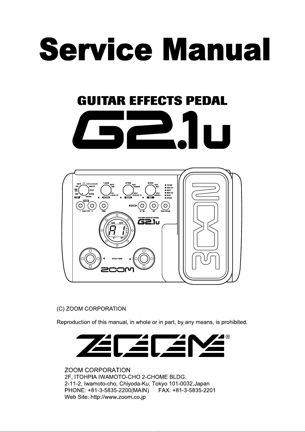
The G2.1u is a multieffect processor with the following features and functions.
●Latest processing technology for outstanding performance
96 kHz / 24 bit sampling (with 32 bit internal processing) assures excellent sound quality. Frequency response
remains flat up to 40 kHz, and input-converted signal-to-noise ratio is an amazing 120 dB, demonstrating the high
level of performance achieved by the G2.1u. The G2.1u also has a USB connection and can be used as a direct
guitar/computer interface.
●Versatile palette of effects including new creations
Out of a total of 54 effects, up to nine (including ZNR) can be used simultaneously. The high-quality choices
provided by the G2.1u include distortion effects that simulate the tones of famous amps and effects pedals, 6-band
guitar EQ and delay effects with "hold" control operated by foot switch.
●Great for live performances and direct recording
The distortion effect module provides two different algorithms for each of its 17 effect types, one for live
performance and one for direct recording. Depending on the on/off setting of the CABINET & MIC effect which
simulates amp cabinet sound and mic characteristics, the most suitable algorithm is automatically selected, giving
you the best sound for any application.
●Integrated rhythm functions and auto-chromatic tuner
A number of rhythm patterns using realistic PCM drum sounds are provided. This is convenient for use as a
metronome during individual practice or to provide a simple rhythm part for a quick session. An auto-chromatic
tuner for guitar is also built right into the unit, allowing you to easily tune your instrument also at home or on stage.
●Sophisticated user interface
The combination of a rotary type selector and three parameter knobs make the effect editing process intuitive and
quick. The mute interval when switching patches has been reduced to less than 5 milliseconds. Seamless patch
changing is now a reality.
●Dual power supply principle allows use anywhere
The G2.1u can be powered from four IEC R6 (size AA) batteries or an AC adapter. Continuous operating time on
batteries is approximately 7.5 hours with alkaline batteries.
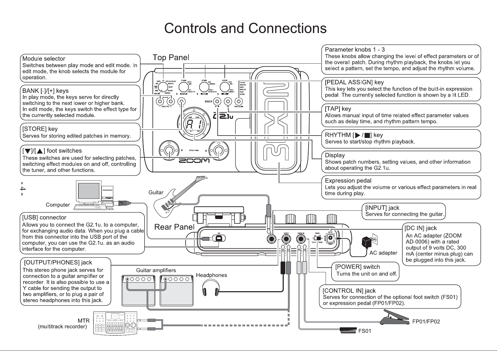
●Easy operation with expression pedal and foot switch
The expression pedal on the top panel lets you adjust the tonal quality of an effect or the volume in real time.
An optional expression pedal (FP01/FP02) or foot switch (FS01) can be connected to the CONTROL IN jack. The
external expression pedal is used for controlling the volume. The foot switch is convenient for quickly toggling
effect programs or for setting the tempo of the rhythm function.
Please take the time to read this manual carefully so as to get the most out of the unit and to ensure optimum
performance and reliability.


- 5 -
Specifications
Effect types 54 types
Effect modules Max. 9 simultaneous modules
Patches User area: 10 patches x 4 banks
Preset area: 10 patches x 4 banks
Sampling frequency 96 kHz
A/D converter 24 bit, 64 times oversampling
D/A converter 24 bit, 128 times oversampling
Signal processing 32 bit
Frequency response 20 Hz - 40 kHz +1 dB -3 dB (with 10 kilohms load)
Display 2-digit 7-segment LED
Parameter LEDs, Pedal assign LEDs
Input Standard mono phone jack
Rated input level -20 dBm
Input impedance 1 megohm
Output Standard stereo phone jack (doubles as line and headphone jack)
Maximum output level Line: +5 dBm (output load impedance 10 kilohms or more)
Phones: 20 mW + 20 mW (into 32 ohms load)
Control input For FP01, FP02, and FS01
USB interface
PC interface: 16-bit (stereo configuration for recording/playback)
Sampling frequency: 32kHz, 44.1kHz, 48kHz
Power requirements
AC adapter 9V DC, 300 mA (center minus plug) (ZOOM AD-0006)
Batteries Four IEC R6 (size AA) batteries,
Approx. 7.5 hours continuous operation (alkaline batteries)
Dimensions 165 mm (D) x 255 mm (W) x 79 mm (H)
Weight 1100 g (without batteries)
Options Expression pedal FP02/ Foot switch FS01
• 0 dBm = 0.775 Vrms
• Design and specifications subject to change without notice.

SDRAM
1M x16bit
DSP
ZFX-3
EMIF
Clock
McBSP
UART1
20MHz
256Fs
CSI0
GPIO
LED
Switch
CPU
(V850/SA1)
24.576MHz
64Fs
1Fs
16bit
Data Bus
Digital In
Digital Out
Port
MIDI I/F
for
Debug/Backup
EEPROM
16kbit
McBSP
7SEG x2figures
Chip LED x6
Tact SWx(8+2)
Port
ADC
11point
VR
Ctrl In
AD0006
DC9V 300mA
BTT level
ROM:256k
RAM:8k
Foot SW/Ex-Pedal
HPI
Encoder
x
3
Ex.Bus
2x8 Matrix
Static Read
1k x16bit
Port
Static Write
+4 for D164
1.Power Supply Block
4.Panel
Block 3.CPU Block
29M33
SW-Reg.
BTT
Linear-Reg.
XC9502
SUM3 x4
+3.3VA
+8VA
+3.3VD
+1.26VD
PC
(USB BUS)
+3.3USBV
Linear-Reg.
XC6213
power switch
+5USBV
2.ANALOG
BLOCK
6.USB
BLOCK
Current Limiter
5.USB Power Supply
Block
BLOCK DIAGRAM
- 6 -
1
6
5
10
5

CODEC
AK4552
64Fs
1Fs
-10dB
+14d
B
0dB
Pre Emphasis
Digital In
Digital Out
96kHz
24bit
ADC
DAC
S/N:97dB
S/N:100dB
Output
GUITAR Input
2.Analog Block
3.CPU Block
+10dB
+10dB
USB CODEC
PCM2904
48kHz
16bit
ADC
DAC
+0dB
+0dB
Pre-emphasis
12MHz
PC
(USB)
data to USB data from USB
De-Emphasis
+6dB
De-emphasis
+6dB
6.USB Block
- 7 -

- 8 -
Description of Block Diagram
1. Power supply block
Power supply
AC Adaptor AD-0006 · +3.3 VD for the CPU, DSP, SDRAM, LEDs including the
7-segment LEDs, and peripherals.
· +1.26 VD for the DSP.
· +3.3 VA for the Analog block.
· +8.0 VA for the Analog block.
2. Analog block
1) Guitar input The signal from [INPUT] jack is sent to the DSP and
processed there.
· Rated input level -20 dBm
· Input impedance 1 megohm
· pre-emphasis +16dB in 40kHz or higher
2) Output Output (For line/headphones)
· Output load impedance
For line: 10 kilohms or higher
For headphone: 20 mW + 20 mW into 32-ohm load
· Maximum output level +5 dBm
· de-emphasis -16dB in 40kHz or higher
· Frequency response Refer to the following figure.
G2.1u Frequency response (Bypass)
INPUT signal-10(dBm)
-30
-25
-20
-15
-10
-5
0
10 100 1000 10000 100000
Frequency (Hz)
OUTPUT LEVEL(dBm)

- 9 -
4) AD/DA converter:
AK4552VT-E2 Sampling frequency 96 kHz
System Clock (256fs) 24.576 MHz
A/D 2-channel
64-times oversampling
24-bit resolution, MSB justified
D/A 2-channel
128-times oversampling
24-bit resolution, LSB justified
3. CPU block
1) CPU
uPD703015BYGC-A29-8EU 32-bit processing microprocessor
(D163-0003) Internal ROM 128 Kbyte
A/D converter 10-bit resolution, 8-channel
Master clock 20 MHz
2) EEPROM:
M93C86-WMN6 16kbit 3-wire
3) DSP: ZFX-3L 32-bit processing
Master clock 24.576 MHz
Bit clock 6.144 MHz (64 fs)
L/R clock 96 kHz (1 fs)
4) SDRAM
IS42S16100C1-7TL 512 K x 16 bit x 2banks, as external memory of the ZFX-3L

- 10 -
4. Panel block STATIC KEY (x 7)
STATIC LED (x 5)
DINAMIC LED (x 6)
ROTARY ENCODER (x3)
11 click VOLUME (x1)
7segment LED (x 1)
All LEDs are lit under the control of the CPU.
5. USB Power Supply block
USB Power Supply
USB BUS Power · +5.0 USBV for the Power supply block.
· +3.3 USBV for the USB block.
· +5.0 VO for the USB block.
6. USB block
AK4552VT-E2 Sampling frequency 48 kHz
System Clock 12 MHz
A/D 2-channel
16-Bit Delta-Sigma ADC and DAC
D/A 2-channel

- 11 -
Back Up User’s Data
If necessary, back up the user’s effect patch data to avoid an accidental erasing.
Required
· User’s G2.1u as a transmitter (hereinafter referred to as “the transmitter”)
· Another G2.1u as a receiver (hereinafter referred to as “the receiver”)
· Jumper wires
1. Remove the bottom plate.
2. Connect “IN” terminal of the transmitter and “OUT” terminal of the receiver.
3. Connect “OUT” terminal of the transmitter and “IN” terminal of the receiver.
4. Connect their ground terminals on the top side of the main PCB, using jumper wires (See
below).
Transmitter Receiver
Main PCB top side Main PCB top side
5. Turn the power of both transmitter and receiver on while holding the [STORE] and the
[RHYTHM] keys.
Make sure that the both 7segment LED lit “tr”.
6. Press the [TYPE -] key of the receiver, and make sure that the 7 segment LED lit “rx”.
The receiver is ready to receive the data.

- 12 -
7. Press the [TYPE +] key of the transmitter and make sure that the 7 segment LED lit “tx”.
The indication flashes on and off at once. And the transmitter starts to send the data.
When sending and receiving finish successfully, and hexadecimals including two dots
such as [x.x.] appears on the display. This displayed [x] depends on User’s patch
conditions.
If [E1] or [E2] or [E3] appear on the display, these mean sending and receiving are error.
In this case, confirm conditions of the transmitter and receiver, and try to back up again.
8. Turn the both transmitter and receiver off.
9. Take the wires away and attach the bottom plate.

- 13 -
Function Test
After repairing, the inspection should be performed with the built-in program for inspection.
※Equipment required
· AC voltage meter (audio analyzer would be better)
· IHF-A filter (audio analyzer might include it)
· Oscillator
· AC adapter (AD-0006)
· Four batteries: R6 [SUM-3] or “AA” size (alkaline batteries are recommended)
· Cables
1. Starting Built-in Inspection Program
Connect the AC-adapter.
Turn on the power holding [TYPE +], [TYPE -], and [RHYTHM] keys.
Starting with TEST-mode, 7segment LED is displayed [8.8.], and all LEDs (except [TYPE +], [TYPE -],
and [STORE] keys) are light up.
2. PLAY / EDIT VOLUME check
Turn the [PLAY] dial clockwise and anticlockwise.
Make sure that the indications “00 -> 01 -> 02 -> 03 -> 04 -> 05 -> 06 -> 07 -> 08 -> 09 -> 0A”
display on the 7segment LED when the dial is turned clockwise.
Make sure that the indications “0A -> 09 -> 08 -> 07 -> 06 -> 05 -> 04 -> 03 -> 02 -> 01 -> 00”
display on the 7segment LED when the dial is turned anticlockwise.
And make sure that only 7segment LED turns on then.
3. DIAL / LED check
Turn the [GAIN] dial, and make sure that the [PATTERN] LED lights up.
Turn the [TONE] dial, and make sure that the [TEMPO] LED lights up.
Turn the [LEVEL] dial, and make sure that the [MIX] LED lights up.
And make sure that the indications “01 ->02 -> 03 ... ->Fd ->FE ->FF” appear on the 7segment
LED display when the dial is turned clockwise, and that “FF ->FE ->Fd ... 02 -> 01 -> 00”
when turned anticlockwise.
4. DSP-MUTE check
Press the [TYPE -] key, and make sure that all LEDs go out and output sound is mute.
Press the [TYPE -] key once more, and all LEDs turn on and output sound is emitted.
5. SRAM check
Press the [TYPE +] key, and make sure that the 7segment LED is displayed [2.P] and the delayed
signal is output from the left channel of [OUTPUT] jack.
6. BATTERY check
Press the [STORE] key, and make sure the 7segment LED is displayed the surveillance level of battery
voltage.

- 14 -
7. SWITCH / LED check
Press the [RHYTHM] key, and make sure that the 7segment LED is displayed [r h].
The [RHYTHM] key turn on and off by pressing the [RHYTHM] key.
Press the [TAP] key, and make sure that the 7segment LED is displayed [t P].
The [TAP] key turn on and off by pressing the [TAP] key.
8. PEDAL ASSIGN check
Press the PEDAL ASSIGN key, and make sure that the 7segment LED is displayed [SL].
And make sure that the PEDAL ASSIGN LED turns on in the order of “VOL ->WAH -> DRY ->MOD
->DLY ->REV -> turns off”, whenever the key is pressed.
9. ANALOG-MUTE check
Press the FOOT SWITCH [▼], and make sure that the 7segment LED is displayed as [mt].
The 7segment LED turns on and off by pressing the FOOT SWITCH [▼].
When the 7segment LED turns on, output sound is extremely low.
10. EEPROM check
Press the FOOT SWITCH [▲], and the status of EEPROM is displayed as the following.
[ok]・・・This indication means that default patch data in the EEPROM is correct.
[E0]・・・This indication means that there are some defective soldering on the EEPROM.
[E1]・・・This indication means that patch data in the EEPROM is false.
11. EX PEDAL check
The 7segment LED is displayed EX PEDAL’s AD value if the PEDAL is moved.
Make sure that this EX PEDAL’s AD value is the same as below table.
Expression pedal Values
MIN(raise) 07 or more
MAX(down) E0 or less
Pushed all the way PEDAL SW ON
Make sure that difference between MIN and MAX is 60 or more in hex and this value doesn’t decrease
if EX PEDAL is pressed down.
Make sure that all PEDAL ASSIGN LEDs are turn on and off by pressing down the EX PEDAL
stronger.
11-1. Adjusting of the Trimmer potentiometer (VR 400)
Open the bottom cover.
With the EX PEDAL fully down, and adjust the value to the range of CE to D2 by rotating the trimmer
potentiometer.

- 15 -
11-2. PEDAL setting
Turn on the power holding the PEDAL ASSIGN key, and the indication “dn” appears on the 7segment
LED. With the EP PEDAL fully raised, press the [STORE] key, and the indication “UP” appears on
the 7segment LED.
And the EP PEDAL fully down and then lift your foot off the pedal, then press the [STORE] key.
And the unit returns to the play mode after the indication [Ok] appears the 7segment LED.
After this setting, make sure that the EX PEDAL’s AD value again.
12. FOOT PEDAL check
Plug the cable from the expression pedal (FP-01/FP-02) to the [CONTROL IN] jack. Make sure that
the 7segment LED is displayed as range [06] to [09] when the FOOT PEDAL is pressed backward,
and make sure that the 7segment LED is displayed as range [E3] to [FF] when the FOOT PEDAL is
pressed forward.
13. FOOT SWITCH (optional) check
Plug the cable from the FS-01 to the [CONTROL IN] jack. Make sure that the 7segment LED is
displayed as range [06] to [09] when the FS-01 is turned on, and make sure that the 7segment LED is
displayed as [00] when the FS-01 is turned off.
14. Battery Warning Check
Set the power supply voltage to 6V. Make sure that the 7segment LED is displayed as [A0] then. And
then set the power supply voltage to 3.9V. Make sure that the 7segment LED is displayed as [bt].
15. Restoring Factory Defaults
Turn the G2.1u on while holding down the [STORE] key, and the indication “AL” appears on the
7segment LED.
Then press the [STORE] key once more, and All Initialize is carried out.
16. TUNER Check
Press both [▼]/[▲] foot switches together briefly and release, and start the tuner mode and the bypass
state. Make sure that then the 7segment LED is displayed as [bp] and the G2.1u is available as the tuner.
17 USB interface operation Check
Connect the unit to PC with USB cable and start up USB inspection software.
In the BYPASS mode, Input sin wave (440Hz/-20dBm) to INPUT jack and monitor the waveform on PC.
And output sin wave (440Hz/-20dBm) from PC, monitor the output from OUTPUT jack (L/MONO, R,
Phones) with speakers and oscilloscope.
*Make sure there are no defects (abnormal noise, output trouble, etc…)
*Refer to “How to use USB inspection software” about the how to use inspection software.
After this function test, carry out all initialization (Refer to page 17).

- -
16
Special Start-up
There are some methods to start up the G2.1u for service.
To start up the unit, set the [POWER] switch to “ON” while holding any keys.
The following table shows which keys are held down.
Keys held down Purposes
Play Mode None Normal operation
Initialization [STORE] Recovering factory default
Test Mode [TYPE +] + [TYPE -] + [RHYTHM] Function test
Data transfer [STORE] + [RHYTHM] Backing up user’s data
Version [UP] Checking software version
Revision [DOWN] Checking software revision
●Play Mode
Normal operation.
See the operation manual.
●Initialization
This startup recovers the factory default condition.
Refer to page 17.
●Test Mode
This startup is used for the function Test.
Refer to page 13-15.
●Data transfer
This startup backs up the user’s effect patch data.
Refer to page 11, 12.
●Version
This startup indicates the software version number.
The indication “0003” appears on the display. (depend on circuit versions)
●Revision
This startup indicates the software revision number.
The indication “9005” appears on the display. (As of October, 2005)

- 17 -
Recovering the Factory Default
In the factory default condition, the patches of the user area (A0-d9) contain the same
settings as the patches of the preset area (00-39). Even after overwriting the user patches,
their original content can be restored in a single operation (“All Initialize” function).
If necessary, back up the user’s patch data. Refer to page 11, 12 for details of the back up.
1. Turn the power on while holding the [STORE] key.
The indication “AL” appears on the display.
2. To carry out the All Initialize function, press the [STORE] key once more.
All patch settings are returned to the factory default condition, and the unit switches to
play mode. To cancel All Initialize, press the [RHYTHM] key instead of the [STORE]
key.

G2.1u Circuit Check Specification
s
No. Items Ch Specifications Inputs Conditions/notes Display and Indicator Keys pressed in "Test mode"
1 Current consumption 190mA±20mA (FLASH uPU) Short Immediately after Test mode starts All LEDs are lit. All lit None (Start up)
180mA±20mA (MASK uPU) Short Immediately after Test mode starts All LEDs are lit. All lit None(Start up)
2 Power supply voltage 3.3VA 3.3V±0.15V Short Immediately after Test mode starts All LEDs are lit. All lit None(Start up)
+3.3VD 3.3V±0.15V Short Immediately after Test mode starts All LEDs are lit. All lit None(Start up)
+1.26VD 1.26V±0.05V Short Immediately after Test mode starts All LEDs are lit. All lit None(Start up)
+8VA 8.74V±1.0V Short Immediately after Test mode starts All LEDs are lit. All lit None(Start up)
3 Output level ( L ) -1.5dBm±1.5dB 440Hz -20dBm Load=32ohms / Output waveform is not clipped. All lit None(Start up)
(Load: 32ohms) ( R ) -4.5dBm±1.5dB 440Hz ±0dBm Load=32ohms / Output waveform is not clipped. All lit None(Start up)
4 Frequency response ( L ) +2.5dBm±1.5dB 20Hz -20dBm Output waveform is not clipped. All lit None(Start up)
(No Load) ( R ) -1.0dBm±1.5dB 20Hz ±0dBm Output waveform is not clipped. All lit None(Start up)
( L ) -16.5dBm±1.5dB 20kHz -40dBm Output waveform is not clipped. All lit None(Start up)
( R ) -20.0dBm±1.5dB 20kHz -20dBm Output waveform is not clipped. All lit None(Start up)
5 Noise level ( L ) -80.0dBm or less Short Insert IHF-A All lit None(Start up)
(No Load) ( R ) -90.0dBm or less Short Insert IHF-A All lit None(Start up)
6 Harmonic distortion ( L ) 0.1% or less 440Hz -5dBm Delay Mode / Insert 20KHz-LPF. "2.P" "Type+" key(SW5)
(No Load) ( R ) 0.1% or less 440Hz -5dBm Delay Mode / Insert 20KHz-LPF. "2.P" "Type+" key(SW5)
7 Function of D-MUTE ( L ) Check function of Mute 440Hz -20dBm Press ”Type-” key and check muting on/off. None ”Type-” key(SW4)
(DSP Mute) ( R ) Check function of Mute 440Hz -20dBm Press ”Type-” key and check muting on/off. None ”Type-” key(SW4)
8 Function of A-MUTE ( L ) Check function of Mute 440Hz -20dBm Press ”Down” key and check muting on/off. "mt" "Down" key(SW9)
(Analog Mute) ( R ) Check function of Mute 440Hz -20dBm Press ”Down” key and check muting on/off. "mt" "Down" key(SW9)
9 Battery warning voltage 4.0V or less (Warning voltage) Make sure that "bt" on display is blinked at 3.9V. "bt" blinked
4.6V or more (released warning) Make sure that the warning is released at 4.7V. Return to normal status
10 Control input Foot sw_OFF 0 FS-01 Make sure that "0" is displayed.
Foot sw_ON 6-9 FS-01 Make sure that value of "6-9" is displayed.
Foot pedal_MIN 6-9 FP-01 Make sure that value of "6-9" is displayed.
Foot pedal_MAX E3-FF FP-01 Make sure that value of "E3-ff" is displayed by hexadecimal.
11 System operation
* Conditions (if there is no note)
Power supply AC adaptor AD-0006
Input signal Sine wave to [INPUT] jack
Output load None (100 kilohms or more)
PHONES: 32 ohms
Make sure that keys, dial(11click), knobs, pedals, EEPROM, and LEDs including display and indicator normally operate.
-18 -

1 2 3 4 56
A
B
C
D
6
54321
D
C
B
A
Title
Number RevisionSize
B
Date: 14-Dec-2005 Sheet of
File: C:\Documents and Settings\inoue\ƒfƒXƒNƒgƒbƒv\19-25-G2.1u Circuit.ddbDrawn By:
5
67
IC8B
NJM2100M
R38
1M
"GUITAR"
C82
10p
L4
open
R39
620
+3.3VA
R41
15k-F
C54 0.1u
R43
75k-F
R42
13k-F
R40
39k-F
+8VA
R13
7.5k
C88
open-c
C97
0.01u film
R36
1.3k
C52
0.1u
3
21
4 8
IC8A
NJM2100M
+
C84
100u/16V
+
C95
10u/16V
+
C94
10u/16V
R46
1k
R47
1k
L6
open
R3
10k
L5
open
C23
open-c
+
C103
10u/16V C58
0.1u
+3.3VA
+ C102
10u/16V C57
0.1u
R35
10
+C96
2.2u/50V
C56
0.1u
5
67
IC7B
NJM4558M
C93
18p
C92
100p
R5
10k
R4
10k +
C90
47u/6.3V
+3.3VA
R20
22k
R21
22k +C91
47u/6.3V
+8VA
C53
open-c
3
21
84
IC7A
NJM4558M
+
C83
0.1u/50V
R80
0
D_OUT
D_IN
D_IN
D_OUT
1FS
1FS
64FS
CODEC_PD- CODEC_PD-
64FS
256FS
256FS
C55
0.1u
RIN
1
LIN
2
VSS
3
VA
4
VD
5
DEM0
6
DEM1
7LRCK 10
MCLK 11
BCLK 12
PDN 13
VCOM 14
LOUT 15
ROUT 16
SDTO
8SDTI 9
IC15
AK4552VT
2
3
1
J3
SJ6336
2
1
4
J2
SJ6335
C98
0.01u
C99
0.01u
R45
1k
R44
1k
C117
1000p
C118
1000p
+
C71
100u/16V
+
C72
100u/16V
+
C86
10u/16V
R22
47k
+8VA C8
0.1u
+
C87
10u/16V
R28
22
R29
22
C22
open-c
R11
22k
R12
22k +C61
47u/6.3V
+8VA
R26
22k
R27
22k
R24
8.2k
C73
1500p
C59
open-c
R23
47k
R25
8.2k
C85
1500p
C60
open-c
3
21
4 8
IC9A
NJM4556M
5
67
IC9B
NJM4556M
R10
22k
R9
22k
1
2
3
4
5
6
7
CN5A
PH-7A (2mmP)
12
D3
1SS133
to USB PCB
R68
47k
"OUTPUT"
CPU
D164_cpu.sch
DSP
D164_dsp.sch
Power
D164_pwr.sch
D164 MAIN PCB(PCB-5155) ANALOGcircuit 1/7
MP
Z3A-0223-A3
Q5
BC817-40LT1G
Q6
BC817-40LT1G
R86
1k
R87
1k
5
43
DT2B
MUN5135DW1T1
2
16
DT2A
MUN5135DW1T1 +8VA
+8VA2
1 3
DT3
DTC124EKA
R85
22k
+8VA
R84
330
12
D8
1SS133
+3.3VD
AMUTE
G2.1uCIRCUIT DIAGRAM
MAINPCB (ANALOG) PCB-5155A
- 19 -

1 2 3 4 5 6 78
A
B
C
D
8
7654321
D
C
B
A
Title
Number RevisionSize
A2
Date: 14-Dec-2005 Sheet of
File: C:\Documents and Settings\inoue\ƒfƒXƒNƒgƒbƒv\19-25-G2.1u Circuit.ddbDrawn By:
/RESET
VSS
1
VDD
2CD 3
OUT 4
IC6
S-80929CNNB-B8P-T2(OPEN)
C74
470p
C16
0.1u
+3.3VD
C1
0.01u
+3.3VD
R1
10k
C17
0.1u
C20
0.1u
BTT_LVL
C13
0.01u
from POWER Section
R74
47k
PORT_D2C
PORT_C2D
DSP_RST-
CODEC_PD-
P21/SO2
1
P22/SCK2
2
P23/RXD1
3
P24/TXD1
4
P25/ASCK1
5
VDD
6
VSS
7
P26/TI2/TO2
8
P27/TI3/TO3
9
P30/TI00
10
P31/TI01
11
P32/TI10
12
P33/TI11
13
P34/TO0/A13
14
P35/TO1/A14
15
P36/TI4/TO4/A15
16
P37/TI5/TO5
17
IC/VPP
18
P100/RTP0/A5
19
P101/RTP1/A6
20
P102/RTP2/A7
21
P103/RTP3/A8
22
P104/RTP4/A9
23
P105/RTP5/A10
24
P106/RTP6/A11
25
P107/RTP7/A12
26
P110/A1
27
P111/A2
28
P112/A3
29
P113/A4
30
RESET
31
P114/XT1
32
XT2
33
VDD
34
X2
35
X1
36
VSS
37
CLKOUT
38
P120/WAIT
39
P90/LBEN/WRL
40
P91/UBEN
41
P92/R/W/WRH
42
P93/DSTB/RD
43
P94/ASTB
44
P95/HLDAK
45
P96/HLDRQ
46
P40/AD0
47
P41/AD1
48
P42/AD2
49
P43/AD3
50
P44/AD4 51
P45/AD5 52
P46/AD6 53
P47/AD7 54
BVDD 55
BVSS 56
P50/AD8 57
P51/AD9 58
P52/AD10 59
P53/AD11 60
P54/AD12 61
P55/AD13 62
P56/AD14 63
P57/AD15 64
P60/A16 65
P61/A17 66
P62/A18 67
P63/A19 68
P64/A20 69
P65/A21 70
AVDD 71
AVSS 72
AVREF 73
P70/ANI0 74
P71/ANI1 75
P72/ANI2 76
P73/ANI3 77
P74/ANI4 78
P75/ANI5 79
P76/ANI6 80
P77/ANI7 81
P80/ANI8 82
P81/ANI9 83
P82/ANI10 84
P83/ANI11 85
P00/NMI 86
P01/INTP0 87
P02/INTP1 88
P03/INTP2 89
P04/NITP3 90
P05/INTP4/ADTRG 91
P06/INTP5/RTPTRG 92
P07/INTP6 93
P10/SI0/SDA 94
P11/SO0 95
P12/SCK0/SCL 96
P13/SI1/RXD0 97
P14/SO1/TXD0 98
P15/SCK1/ASCK0 99
P20/SI2 100
IC1
uPD703015BYGC-A29-8EU
C18
0.1u
C77
open-c
C76
open-c
AVSS
AVDD
+3.3VD
DEBUG
R31
1k
R33
1k
C14
0.01u
R32
1k
C11
0.01u
CPUD0
CPUD1
CPUD2
CPUD3
CPUD4
CPUD5
CPUD6
CPUD7
SCAN0
SCAN1
1
5
2
3
4
8
7
6
RA2
47k*4
1
5
2
3
4
8
7
6
RA1
47k*4
+3.3VD
C19
0.1u
R30
1k
C12
0.01u
AVSS
L1
0 ohm
R54
1k
R53
470k
R52
10k
C15
0.1u
2
1
3
D1
1SS226(OPEN)
L3
0 ohm
"FOOT-SW/EX-PEDAL"
L2
0 ohm
R51
330k
CONTROL_VAL
DSP_HAS-
DSP_HDS-
DSP_R/W-
DSP_RDY
R56
open-r
R57
open-r
+C67
100u/6.3V
+3.3VD
CPUD[0..7]
CPUD[0..7]
AVSS AVDD
1
5
2
3
4
8
7
6
RA4
47k*4
1
5
2
3
4
8
7
6RA3
47k*4
2
16
DT1A
MUN5135DW1T1
5
43
DT1B
MUN5135DW1T1
TP1
TEST_MODE
R64
47k
R63
open-r
+3.3VD
+3.3VD
R62
47k
CS
1
CLK
2
DI
3
DO
4VSS 5
ORG 6
VCC 8
PE 7
IC14
IS93C86A-3GRLI
AVDD
AVSS
2
3
1
J1
SJ6336
+3.3VD
LED0
LED1
LED2
LED3
LED4
LED5
LED6
LED7
LED8
LED9
LED10
1
2
3
X1
20MHz
TP3
IN
TP4
OUT
R72
47k R73
47k
+3.3VD
1
2
3
4
5
CN3A
PH-5A (2mmP)
AVSS
AVDD
LED8
LED9
LED10
LED_COM0
LED_COM1
LED_COM0
LED_COM1
LED[8..10]
PEDAL_VAL
SW_PEDAL
SW_SELECT
SW_PEDAL
SW_SELECT
TP5
GND
1
2
3
CN2A
PH-3A(2mmP)
R14
22k R15
22k
C2
0.039u
C3
0.027u
R16
22k R17
22k
C4
0.039u
C5
0.027u
R18
22k R19
22k
C6
0.039u
C7
0.027u
ECA_GAIN
ECB_GAIN
ECA_TONE
ECB_TONE
ECA_LEVEL
ECB_LEVEL
SW_TAP
SW_RHYTHM
SW_STORE
SW_TYPEP
SW_TYPEM
SW_UP
SW_DOWN
1
2
3
CN7A
PH-3A (2mmP)
1
2
3
4
5
6
7
8
9
10
11
12
13
14
15
16
17
18
19
20
CN9A
11311120-13420000
+3.3VD
1
2
3
4
5
6
7
8
9
10
CN8A
PH-10A (2mmP)
LED0
LED1
LED2
LED3
LED4
LED5
LED6
LED7
LED_COM0
LED_COM1
LED_GAIN
LED_TONE
LED_LEVEL
LED_RHYTHM
LED_TAP
TO VR-PCB
TO FOOTSW-PCB
TO 7SEG-PCB
TO PANEL-PCB
TO PEDAL-PCB
TO PEDAL-PCB
1
2
3
4
5
6
7
CN4A
PH-7A(2mmP)
+3.3VD
R2
0
ECA_GAIN
ECB_GAIN
ECA_TONE
ECB_TONE
ECA_LEVEL
ECB_LEVEL
SW_TAP
SW_RHYTHM
SW_STORE
SW_TYPEP
SW_TYPEM
LED_GAIN
LED_TONE
LED_LEVEL
LED_RHYTHM
LED_TAP
1
2
3
4
5
6
7
8
CN10
11310808-13440000(open)
+3.3VD
1
2
3
4
5
6
7
8
9
10
11
12
13
14
15
16
17
18
19
20
D163
12 D6
1SS133(OPEN)
1 2
D7
1SS133(OPEN)
+3.3VD
VDD
1
VSS
2CD 3
OUT 4
IC4
R3112Q291A
For Flash-Writer
To CN9A
MP
Z3A-0223-A3
AMUTE
D164
D164 MAIN PCB(PCB-5155) CPU circuit 3/7
D164MP_cpusch
D164 MAIN PCB(PCB-5155) ANALOG circuit 1/7
MP
Z3A-0223-A3
G2.1u CIRCUIT DIAGRAM
MAIN PCB (CPU) PCB-5155A
-20 -
Other manuals for G2.1u
1
Table of contents
Other Zoom Music Pedal manuals

Zoom
Zoom B1on User manual

Zoom
Zoom Multistomp MS-70CDR User manual

Zoom
Zoom MultiStomp MS-50G User manual

Zoom
Zoom 508 User manual

Zoom
Zoom G1 Four User manual

Zoom
Zoom 505 guitar User manual

Zoom
Zoom 503 AMP SIMULATOR User manual

Zoom
Zoom G6 User manual

Zoom
Zoom Tri Metal TM-01 User manual

Zoom
Zoom 504 Acoustic User manual