Acute ADP1025 User manual
i
Acute Technology Inc. Copyright 2016
High Voltage Differential Probe user's manual
ADP1025 25MHz/700Vpk
ADP2025 25MHz/1400Vpk

ii
Acute Technology Inc. Copyright 2016
T
Ta
ab
bl
le
e
o
of
f
C
Co
on
nt
te
en
nt
ts
s
G
Ge
en
ne
er
ra
al
l
S
Sa
af
fe
et
ty
y
S
Su
um
mm
ma
ar
ry
y
-
--
--
--
--
--
--
--
--
--
--
--
--
--
--
--
--
--
--
--
--
--
--
--
--
--
--
--
--
--
--
--
--
--
--
--
--
--
--
--
--
--
--
--
--
--
--
--
--
--
--
--
--
--
--
--
--
-
1
1
Safety Instructions ---------------------------------------------------------------------------------------- 1
Symbols and Terms--------------------------------------------------------------------------------------- 3
C
Co
om
mp
pl
li
ia
an
nc
ce
e
&
&
C
Ce
er
rt
ti
if
fi
ic
ca
at
ti
io
on
n
-
--
--
--
--
--
--
--
--
--
--
--
--
--
--
--
--
--
--
--
--
--
--
--
--
--
--
--
--
--
--
--
--
--
--
--
--
--
--
--
--
--
--
--
--
--
--
--
--
--
--
--
--
--
-
4
4
I
In
nt
tr
ro
od
du
uc
ct
ti
io
on
n
-
--
--
--
--
--
--
--
--
--
--
--
--
--
--
--
--
--
--
--
--
--
--
--
--
--
--
--
--
--
--
--
--
--
--
--
--
--
--
--
--
--
--
--
--
--
--
--
--
--
--
--
--
--
--
--
--
--
--
--
--
--
--
--
--
--
--
--
--
--
--
--
--
--
--
-
7
7
Application--------------------------------------------------------------------------------------------7
Probe Appearance------------------------------------------------------------------------------------8
Accessories-------------------------------------------------------------------------------------------10
S
Sp
pe
ec
ci
if
fi
ic
ca
at
ti
io
on
ns
s
-
--
--
--
--
--
--
--
--
--
--
--
--
--
--
--
--
--
--
--
--
--
--
--
--
--
--
--
--
--
--
--
--
--
--
--
--
--
--
--
--
--
--
--
--
--
--
--
--
--
--
--
--
--
--
--
--
--
--
--
--
--
--
--
--
--
--
--
--
--
--
-
1
12
2
O
Op
pe
er
ra
at
ti
io
on
n
-
--
--
--
--
--
--
--
--
--
--
--
--
--
--
--
--
--
--
--
--
--
--
--
--
--
--
--
--
--
--
--
--
--
--
--
--
--
--
--
--
--
--
--
--
--
--
--
--
--
--
--
--
--
--
--
--
--
--
--
--
--
--
--
--
--
--
--
--
--
--
--
--
--
--
--
--
-
1
13
3
Connecting the probe to the instrument with input impedance of 1 MΩ --------------------13
Connecting the probe to the test circuit-----------------------------------------------------------14
Operation with Oscilloscope -----------------------------------------------------------------------15
Offset null adjusting---------------------------------------------------------------------------------15
Bandwidth Limit-------------------------------------------------------------------------------------16
O
Op
pe
er
ra
at
ti
in
ng
g
B
Ba
as
si
ic
cs
s
-
--
--
--
--
--
--
--
--
--
--
--
--
--
--
--
--
--
--
--
--
--
--
--
--
--
--
--
--
--
--
--
--
--
--
--
--
--
--
--
--
--
--
--
--
--
--
--
--
--
--
--
--
--
--
--
--
--
--
--
--
--
--
--
--
--
--
-
1
17
7
Overrange Detection --------------------------------------------------------------------------------17
Common-Mode Rejection --------------------------------------------------------------------------17
Twisting the Input Leads ---------------------------------------------------------------------------17
Probe Loading----------------------------------------------------------------------------------------17
F
Fu
un
nc
ct
ti
io
on
na
al
l
C
Ch
he
ec
ck
k
-
--
--
--
--
--
--
--
--
--
--
--
--
--
--
--
--
--
--
--
--
--
--
--
--
--
--
--
--
--
--
--
--
--
--
--
--
--
--
--
--
--
--
--
--
--
--
--
--
--
--
--
--
--
--
--
--
--
--
--
--
--
--
--
--
--
-
1
18
8
P
Pe
er
rf
fo
or
rm
ma
an
nc
ce
e
V
Ve
er
ri
if
fi
ic
ca
at
ti
io
on
n
-
--
--
--
--
--
--
--
--
--
--
--
--
--
--
--
--
--
--
--
--
--
--
--
--
--
--
--
--
--
--
--
--
--
--
--
--
--
--
--
--
--
--
--
--
--
--
--
--
--
--
--
--
--
--
-
1
19
9
1
Acute Technology Inc. Copyright 2016
General Safety Summary
Safety Instructions
Read the safety instructions to avoid injury and prevent damage to this product or any
products connected to it.
Ground the product.
This probe is grounded with the shell of BNC connector, through the grounding
conductor of the power cord of the measurement instrument.
To avoid electric shock, the grounding conductor must be connected to earth ground.
Before making connections to the input leads of this probe, ensure that the output BNC
connector is attached to the BNC connector of the measurement instrument, while the
measurement instrument is properly grounded.
Observe all terminal ratings.
To avoid shock hazard or fire, please note all ratings and markings on the product.
Check the product manual for further ratings information before making connections to
the product.
Do not connect a potential to any terminal that exceeds the maximum rating of that
terminal.
Connect and disconnect properly.
Do not connect/disconnect probes and test leads while they are connected to a potential
source.
Connect the probe output to the measurement instrument before connecting the probe to

2
Acute Technology Inc. Copyright 2016
the circuit under test.
Disconnect the probe input leads from the circuit under test before disconnecting the
probe from the measurement instrument.
Do not operate in wet/damp conditions.
Do not operate in an explosive atmosphere.
Keep product surfaces clean and dry.
3
Acute Technology Inc. Copyright 2016
Symbols and Terms
These symbols & terms may appear in this manual or on the product to alert you to important
safety considerations.
DANGER indicates an injury hazard immediately accessible as you read the
marking.
Danger statements identify conditions or practices that could result in injury or loss
of life.
WARNING indicates an injury hazard not immediately accessible as you read the
marking. Warning statements identify conditions or practices that could result in
damage to this product or other property.
Double insulation
Earth (ground) Terminal

4
Acute Technology Inc. Copyright 2016
Compliance & Certification
This section lists the EMC, safety, and environmental standards with which the probe
complies.
EMC Compliance:
EC Declaration of Conformity –EMC
Meets intent of Directive 2004/108/EC & 2014/30/EU for Electromagnetic
Compatibility.
Compliance was demonstrated to the following specifications as listed in the Official
Journal of the European Communities:
EN 61326-1:2013, EN 61326-2-1:2013. EMC requirements for electrical equipment for
measurement, control, and laboratory use.
EN55011:2009/A1:2010. Radiated and conducted emissions, Group 1, Class B
IEC 61000-4-2:2008. Electrostatic discharge immunity (ESD)
IEC 61000-4-3:2008. RF electromagnetic field immunity (RS)
IEC 61000-4-4:2012. Electrical fast transient/burst immunity (EFT)
IEC 61000-4-5:2005. Power line surge immunity
IEC 61000-4-6:2008. Conducted RF immunity
IEC 61000-4-8:2009. Power frequency magnetic field immunity
IEC 61000-4-11:2004. Voltage dips and interruptions immunity
EN 61000-3-2:2006. AC power line harmonic emissions
EN 61000-3-3:2013. Voltage changes, fluctuations, and flicker
Safety Compliance:
Equipment Type: Differential Voltage Probe
EC Declaration of Conformity –Low Voltage
Compliance was demonstrated to the following specification as listed in the Official
Journal of the European Communities:

5
Acute Technology Inc. Copyright 2016
Low Voltage Directive 2006/95/EC.
EN 61010-031/A1:2008. Safety requirements for electrical equipment for measurement,
control and laboratory use –Part
031: Safety requirements for handheld probe assemblies for electrical measurement and
test.
Pollution Degree Description:
A measure of the contaminants that could occur in the environment around and within a
product. Typically the internal environment inside a product is considered to be the same
as the external. Products should be used only in the environment for which they are
rated.
Pollution Degree 1.
No pollution or only dry, nonconductive pollution occurs. Products in this category are
generally encapsulated, hermetically sealed, or located in clean rooms.
Pollution Degree 2.
Normally only dry, nonconductive pollution occurs. Occasionally a temporary
conductivity that is caused by condensation must be expected. This location is a typical
office/home environment. Temporary condensation occurs only when the product is
out of service.
Pollution Degree 3.
Conductive pollution, or dry, nonconductive pollution that becomes conductive due to
condensation.
These are sheltered locations where neither temperature nor humidity is controlled. The
area is protected from direct sunshine, rain, or direct wind.
Pollution Degree 4.
Pollution that generates persistent conductivity through conductive dust, rain, or snow.
Typical outdoor locations.
Pollution Degree
Pollution Degree 2 (as defined in IEC 61010-1). Note: Rated for indoor use only.
Installation & Measurement (Overvoltage) Category Descriptions
Terminals on this product may have different installation or measurement (overvoltage)

6
Acute Technology Inc. Copyright 2016
category designations. The installation and measurement categories are:
Measurement Category IV. For measurements performed at the source of low-voltage
installation.
Measurement Category III. For measurements performed in the building installation.
Measurement Category II. For measurements performed on circuits directly connected to
the low-voltage installation.
Measurement Category I. For measurements performed on circuits not directly connected
to MAINS.
Overvoltage Category (AC Adapter)
Overvoltage Category II (as defined in IEC 61010-1)
7
Acute Technology Inc. Copyright 2016
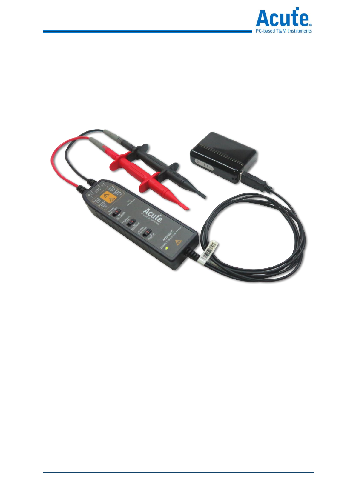
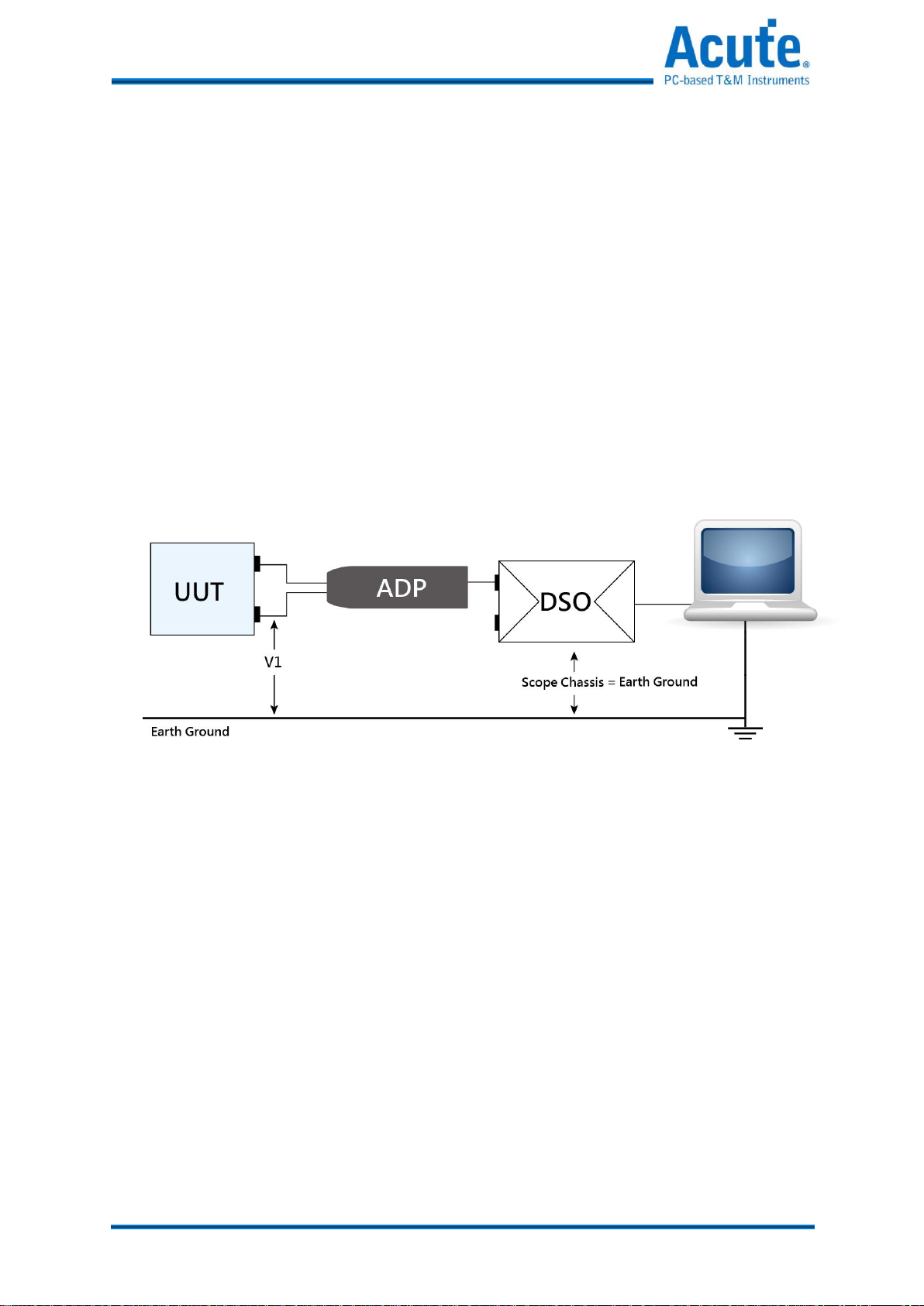
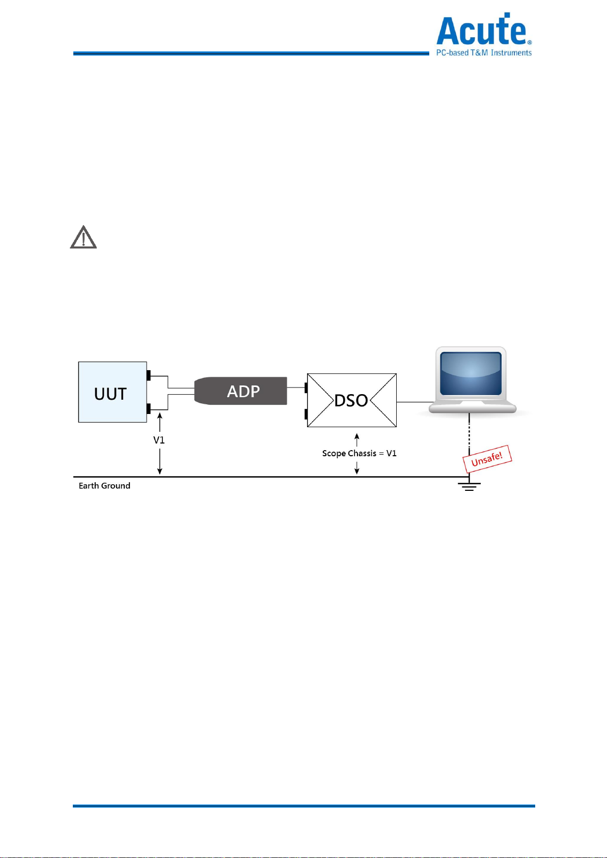
Introduction
The ADP can be used with any oscilloscope and enables users to safely make measurements
of floating circuits with their oscilloscope grounded. The ADP Active Differential Probe
converts floating signals to low-voltage ground-referenced signals that can be displayed
safely and easily on any ground-referenced oscilloscope.
WARNING: For safe operation, do not use the ADP High-voltage Differential Probe
with oscilloscopes that have floating inputs (isolated inputs). The ADP High-voltage
Differential Probe requires an oscilloscope or other measurement instrument with grounded
inputs.
Application
Floating Measurements
Switching Power Supply Design
Motor Drive Design
Electronic Ballast Design
CRT Display Design
Power Converter Design and Service
Power Device Evaluation
Set each channel as Add A Signal.

8
Acute Technology Inc. Copyright 2016
Probe Appearance
DANGER. The rated working voltage with higher Measurement Category probably occurs a
huge surge. To avoid risk of electric shock or fire, do not exceed category rating of the
probe.
WARNING. To avoid risk of electric shock or fire, do not exceed either the voltage rating
or category rating of the probe or the probe accessory, whichever is the lesser of the two.
WARNING: For safe operation, do not use the ADP High-voltage Differential Probe
with oscilloscopes that have floating inputs.
Controls and Indicators
The probes have several features that make probing and measurement a simpler task.
Depending on the probe model, your probe attenuation ranges may differ from those
illustrated.

9
Acute Technology Inc. Copyright 2016
Overrange Indicator
The Overrange indicator lights red if the voltage of the input signal exceeds the linear range
of the range setting.
When this happens, the signal on the probe output does not accurately represent the signal
on the probe input.
Range Switch (Attenuation Switch)
Switch the voltage range (attenuation) settings of the probe. The range should be adjusted
on the oscilloscope.
The Overrange LED lights if the applied voltage exceeds the selected range. To extinguish
the LED, select a higher range.
If a higher range is not available, do not attempt to take the measurement with the probe.
Bandwidth Limit Switch
Switch to 5MHz will limit the probe bandwidth below 5 MHz. 5 MHz is close to the
switching frequency of most switching transistors (FETs) in switch mode power supplies
(SMPS).
The 5MHz filter assists in the characterization and testing of power supplies in switch
mode by removing all high frequency content, noise and harmonics from the measurement.
Audible Overrange Switch
Switch on to enable an audible alarm that indicates when the measured signal exceeds the
selected range.
Offset null trimmer (Offset cover on the bottom side)
There are 3 offset trimmers for nulling the DC-offset drift.
1. 10X/100X Coarse trimmer for both 10X/100X (or 20X/200X, 50X/500X) offset nulling.
2. 10X Fine-trimmer for 10X (or 20X, 50X) offset nulling.
3. 100X Fine-trimmer for 100X (or 200X, 500X) offset nulling.
WARNING. To avoid risk of electric shock or fire, do not open the offset-cover as the
probe connecting to any under testing circuit or signal.
10
Acute Technology Inc. Copyright 2016
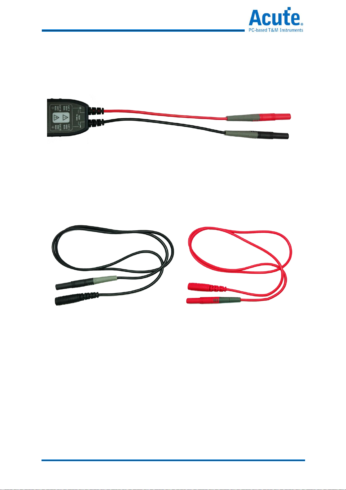
Accessories
Integral Input Leads
The integral input leads extend ~9 in (0.23 m) from the probe body. Connect the leads
directly to your circuit, or use the extender leads and the accessories shown below.
Extender Leads
These cables extend the reach of the probes by ~67 in (1.5 m). The banana ends connect to
all of the clip accessories that are included with the probes. One pair of extender leads are
included with the probes.
Maximum ratings: 2300 V CAT I * 1000 V CAT III
Hook Clips (AC280-FL)
Plug the probe test leads into the banana plug connectors. Squeeze the grips to expose the
hook clip and then clasp it around the circuit test point.
Maximum ratings: 1000 V CAT III, 600 V CAT IV One pair of hook clips is included with
the probes.

11
Acute Technology Inc. Copyright 2016
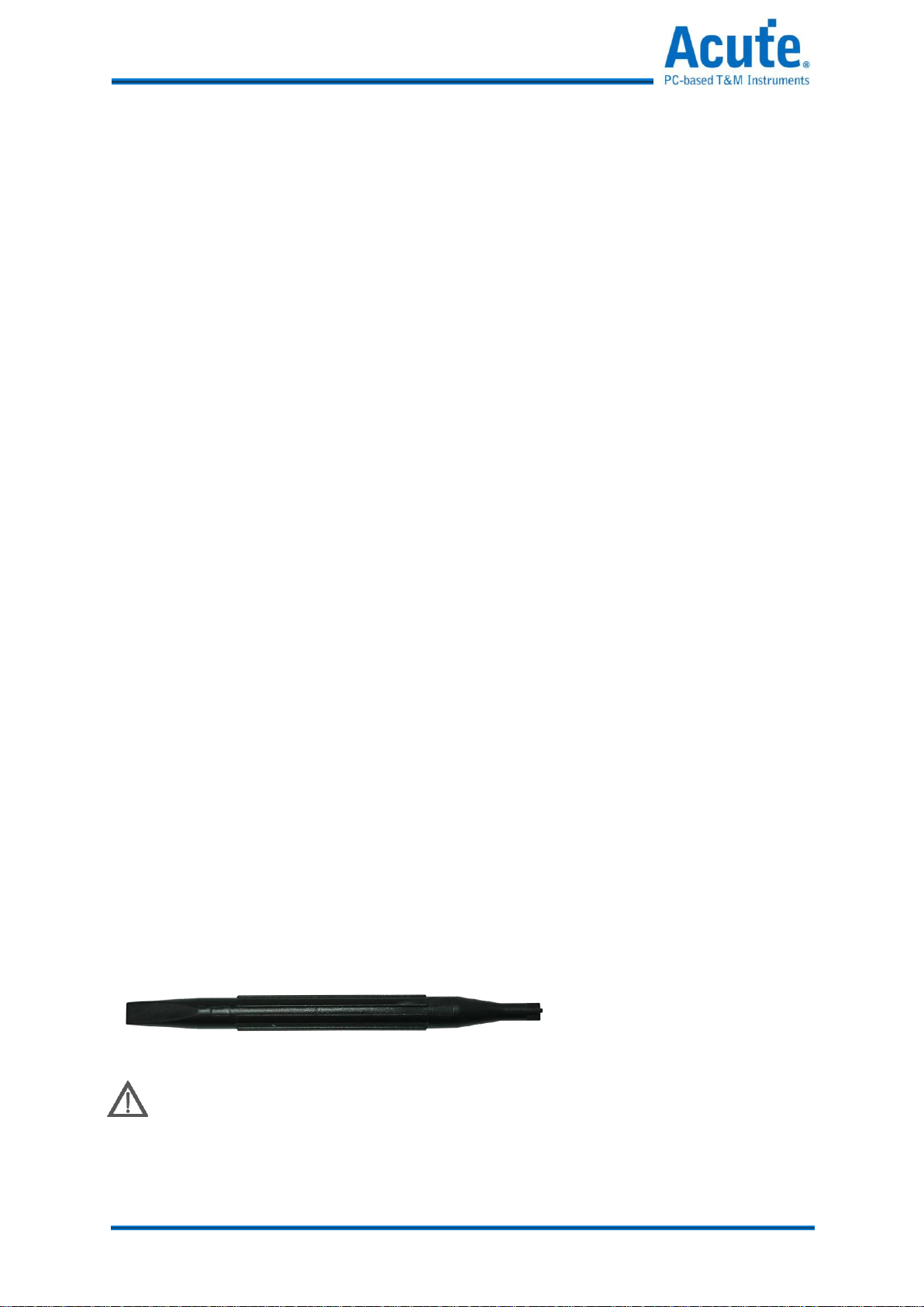
Adjusting Tool (PF-903)
The screwdriver with Slot-end is for opening Offset-cover, and with Frierson-end is for
adjusting trimmer.
WARNING. To avoid risk of electric shock or fire, do not exceed either the voltage
rating or category rating of the probe or the probe accessory, whichever is the lesser of the
two.

12
Acute Technology Inc. Copyright 2016
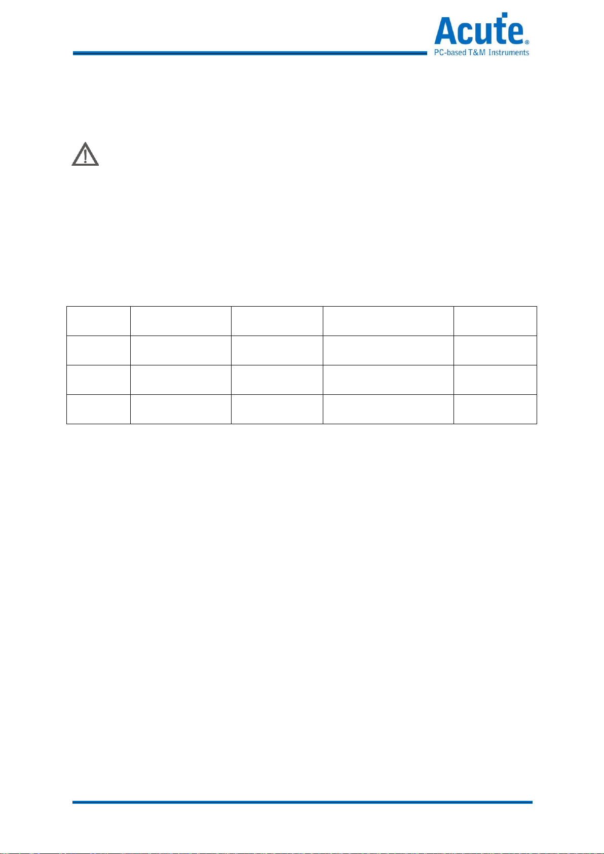
Specifications
Specification
ADP-1025
ADP-2025
Bandwidth (-3dB)
DC to 25MHz
Attenuation
1:10/100
1:20/200
Gain accuracy
±2%
Offset zero (Scope gain=1X)
±10 mV
Diff. Input Impedance
10Mohm, 1pF
Rise time (small signal, 10-90%, 20-30°C)
14ns
Input voltage
Diff. Vin
100X: ±700V
(DC+ pk AC)
10X: ±70V
(DC + pk AC)
200X: ±1400V
(DC + pk AC)
20X: ±140V
(DC + pk AC)
Comm. Vin
±700V
±1400V
Max. Vin to Earth
600V CAT-II ;
300V CAT-III
1000V CAT-II ;
600V CAT-III
Impulse withstand
2500V
4000V
CMRR (typical)
DC: > 80dB
100kHz: > 60dB
1MHz: > 50dB
10MHz: > 38dB
Output swing
±7V (to 1Mohm load)
Offset adjusting range (Scope gain=1X)
Coarse: ±150mV
Coarse: ±150mV
Fine: ±30mV
Bandwidth limit filters
-3dB @ ~5MHz
Diff. overvoltage detection level
100X: > |±700| V
200X: > |±1400| V
10X: > |±70| V
20X: > |±140| V
Temperature
Operating
0°C to 40°C (32°F to 104°F)
Storage
-30°C to 70°C (-22°F to 158°F)
Humidity
Operating
0°C to 35°C (32°F to 95°F), 0 to 85% RH
Storage
-55°C to 60°C (-67°F to 140°F), 0 to 90% RH
Power requirement
USB (5V, < 250mA)
Body dimension (L,W,H)mm3
145,45,20
Weight (Probe body only)
180g
Length of BNC/USB-cable
90cm
Length of Lead-cable
24cm

13
Acute Technology Inc. Copyright 2016
Operation
Connecting the probe to the instrument with input impedance of 1 MΩ
The probe requires an external 5Vdc power. Install the probe as follows:
1. Connect the output of the probe to the BNC input of the test instrument. The test
instrument must be ground (not floating).
2. Connect the power cord to the USB power source.
3. The green LED of the probe light to confirm power-on.
4. Adjust the vertical offset (or position).
5. Select the proper range setting.
ex, when using the ADP2025 probe, to achieve higher resolution and less noise when
measuring signals below 140V pk, switch the attenuation to 20X. If the Overrange
indicator lights or flashes, the output signal may not be accurate.
Use the 200X setting instead.
WARNING. To avoid electrical shock, observe proper safety precautions when
working with voltages above 60 VDC or 30 VACRMS.
These voltage levels pose a shock hazard. Use only the accessories specified for the
probe that you are using.
Make sure that the accessories are fully mated before connecting or disconnecting.
WARNING. To avoid electrical shock or fire, make sure the test leads are in good
condition.
If the wire jacket becomes excessively worn, do not use the probe.
6. Using the appropriate probe accessories, connect the inputs of the probe to the circuit
points to be measured.
WARNING. To avoid electrical shock or fire, keep the output cable of the probe
away from the circuits being measured. The output cable is not intended to be in contact
with the circuits being measured.

14
Acute Technology Inc. Copyright 2016
Connecting the probe to the test circuit
Two inputs are available at the probe tip to connect the probe to a circuit under test.
For accurate measurements, the + and –inputs both must always be connected to the test
circuit.
Positive voltages applied to the + input (red) relative to the –input (black) will deflect the
oscilloscope trace toward the top of the screen.
To maintain the high performance capability of the probe in measurement applications,
care must be exercised in connecting the probe to the test circuit.
Increasing the parasitic capacitance or inductance in the input paths may introduce a “ring”
or may slow the rise time of fast signals.
Input leads that form a large loop area will pick up any radiated electromagnetic field that
passes through the loop and may induce noise into the probe inputs.
Because this signal will appear as a differential mode signal, the probe’s common mode
rejection will not remove it.
This effect can be greatly reduced by twisting the input leads together to minimize the loop
area.
High common mode rejection requires precise matching of the relative gain or attenuation
in the + and –input signal paths.
Mismatches in additional parasitic capacitance, inductance, delay, and a source impedance
difference between the + and –signals will lower the common mode rejection ratio.
Therefore, it is desirable to use the same length and type of wire and connectors for both
input connections.
When possible, try to connect the inputs to points in the circuit with approximately the
same source impedance.
15
Acute Technology Inc. Copyright 2016
Operation with Oscilloscope
When the probe is connected to a oscilloscope, the displayed scale factor and measurement
values will be adjusted to account for the effective gain of the probe.
Through the oscilloscope software, the probe’s internal attenuation and offset can be
conveniently controlled through the oscilloscope’s user interface.
Turning the VOLTS/DIV knob will control the oscilloscope’s scale factor and the probe’s
internal attenuation to give full available dynamic range.
Some of the transition of the scale factor will result in a change of attenuation.
Offset null adjusting
The probe has offset capability. This allows you to remove a DC bias voltage from the
differential input signal while maintaining DC coupling.
The offset range of the probe is a function of the oscilloscope’s attenuation.
Some DC offset drift may occur from thermal effects and different power-ground loop.
The probe must have a warm-up period of at least 20 minutes and be in an environment that
does not exceed the limits described.
There are 3 offset trimmers for nulling the offset drift:
1. 10X/100X Coarse trimmer for both 10X/100X (or 20X/200X, 50X/500X) offset null.
2. 10X Fine-trimmer for 10X (or 20X, 50X) offset null.
3. 100X Fine-trimmer for 100X (or 200X, 500X) offset null.
After 20 minutes warm-up, you may switch 10X/100X (or 20X/200X, 50X/500X)
attenuation path to check their offset drift via oscilloscope.
If the offset drift exists on either attenuation path, you may open the Offset-cover by using
the Slot-end of the adjusting tool(PF-903).
WARNING. To avoid risk of electric shock or fire, do not open the offset-cover as the
probe connecting to any under testing circuit or signal.

16
Acute Technology Inc. Copyright 2016
Adjust the trimmers by using the Frierson-end of the adjusting tool(PF-903).
The skill of adjusting:
1. Make sure the probe already warm-up for over 20 minutes.
2. Disconnect the probe to any under testing circuit. Short the positive and negative input
probes.
3. Place to the center position of both Fine-trimmers
4. If the DC-offset of both attenuation path all toward positive or negative position, adjust
the Coarse-trimmer until either one is positive and another one is negative.
5. Adjust Fine-trimmer to null the DC offset of each attenuation path
Bandwidth Limit
To comply with various test standards used for quantifying output noise of power supplies,
the probe is capable of switching the bandwidth limit from full bandwidth to 5 MHz.

17
Acute Technology Inc. Copyright 2016
Operating Basics
Overrange Detection
Differential voltage outside the operating range will overdrive the circuitry of the probe and
distort the output signal. When this differential Overrange occurs, the probe detects the
condition and lights the Overrange indicator. With the Audible Overrange ON, the probe
will also emit an audible alarm.
Common-Mode Rejection
The common-mode rejection ratio (CMRR) is the specified ability of a probe to reject
signals that are common to both inputs.
More precisely, CMRR is the ratio of the differential gain to the common-mode gain. The
higher the ratio, the greater the ability of probe to reject common-mode signals.
Common mode rejection decreases as the input frequency increases. For example, if you
apply a 60 Hz line voltage of 500 Vp-p to both input leads of the probe, the probe rejects
the signal by 80 dB (typical) and the signal appears as only a 50 mVp-p signal on the
oscilloscope screen.
Twisting the Input Leads
Twisting the input leads helps to cancel noise that is induced into the input leads and to
improve the high frequency response of the inputs.
Probe Loading
When you touch your probe tip to a circuit element, you are introducing a new resistance,
capacitance, and inductance into the circuit. Frequency and impedance of the source
determine how much the probe loads the circuit you are measuring. As the frequency of the
source starts to increase beyond 1 kHz, the input impedance of the probe begins to
decrease.
The lower the impedance of the probe relative to that of the source, the more the probe
loads the circuit under test. For a graph of frequency versus input impedance, refer to the
Specifications section. As the graph shows, the probes have virtually no loading effect on
sources with relatively low impedance and low frequency.
18
Acute Technology Inc. Copyright 2016
Functional Check
Using accessories that are shipped with your probe and a source that supplies AC line voltage,
perform the following
WARNING. To reduce risk of shock or fire, ensure that the accessories are fully
mated before you connect to voltage sources above 42 Vpk.
1. Connect the output of the probe to the oscilloscope input channel.
2. Connect the probe inputs to the AC voltage source.
3. Connect the inputs, set the voltage range, and perform the check as each row of the
following table indicates.
Input 1
Input 2
Mode
Range setting
Check
Hot
Ground/Neutral
Differential
High (500/200/100x)
(A)
Hot
Ground/Neutral
Differential
Low (50/20/10x)
(B)
Hot
Hot
Common
High/Low
No
signal 11 If a DC offset voltage is present, null the DC-offset. (See Offset Null adjusting
section.)
(A)Measurement instrument displays or indicates the line voltage
(B)Measurement instrument displays or indicates the line voltage. Overrange indicator lights
if the input is ~20% over
This manual suits for next models
1
Table of contents
Other Acute Test Equipment manuals


