Aetina ACE-N622 User manual

i
User Manual
Nvidia Jetson Series Carrier board
Aetina ACE-N622

ii
Document Change History
Version
Date
Description
Authors
V1 2018/05/23 Initial Release. Eric Chu
V2
2018/06/22
Specification change
Eric Chu

- 1 -
1. Introduction
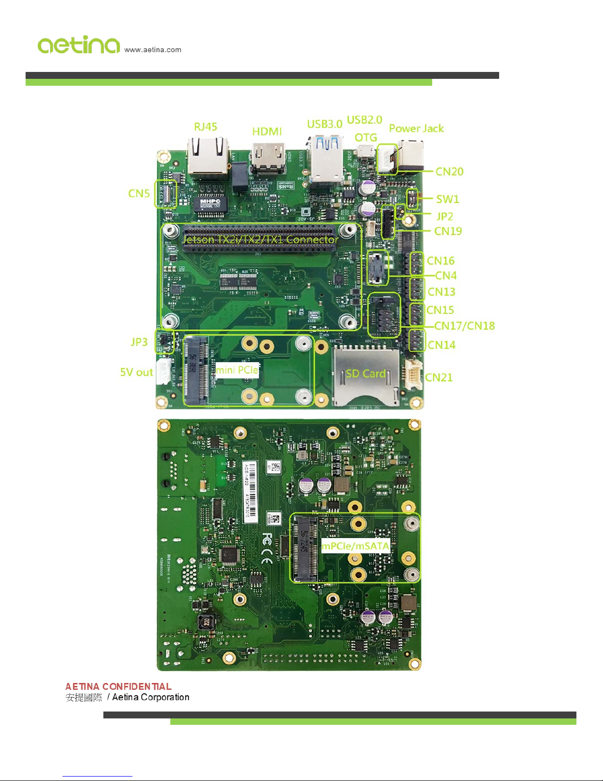
ACE-N622 is a standard Nano-ITX form factor carrier board. Support for NVIDIA® Jetson™
TX2 and Jetson™ TX1. You can quickly emulate the functionality of your desired end
product for software development and hardware verification.
To build a functional prototype of your target system you will need:
•Nvidia TX1/TX2/TX2i module
(Aetina’s P/N: NSO-MD-TX1/NSO-MD-TX2/NSO-MD-TX2i)
•Nano-ITX carrier board (Aetina’s P/N: ACE-N622)
•Power adaptor 12-19 DC/5A
1.1 Features
•Specifically designed for high performance and low-power envelope AI computing
Additional driver to support Embedded peripheral modules for multiple I/O
expansion capability
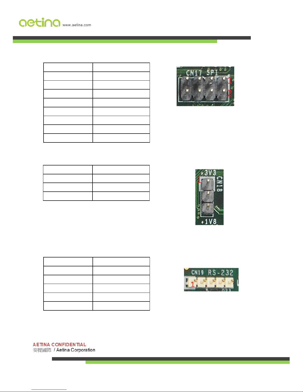
•On-board 1x HDMI, 2x CAN Bus, 4x GPIO, 1x RS232, 1xI2C and 2x Full-Mini Cards to
support rich multimedia and MIPI CSI camera
•Extended temperature range -20°C to 70°C
•Suitable for general robotics, UAV, industrial inspection, medical imaging and deep
learning
•12V / 5V output to support mPCIe extension module.
1.2 Board
•6-layer printed circuit board(PCB)
•Phsical dimensions: 120mm x 120mm
•High-Bandwidth Digital Content Protection (HDCP) support

- 2 -
2. Board Specification
Specification
ACE-N622 Description
Module Compatibility Nvidia Jetson TX1 / Nvidia Jetson TX2 / Nvidia Jetson TX2i
GPU
Jeston TX1 :
-Nvidia MaxwellTM, 256 CUDA cores.
Jetson TX2 :
-Nvidia PascalTM, 256 CUDA cores.
Jetson TX2i(Industrial Grade) :
-Nvidia PascalTM, 256 CUDA cores.
CPU Jetson TX1 :
-Quad ARM® A57/2MB L2
Jetson TX2 :
-HMP Dual Denver 2/2MB L2 + Quad ARM® A57/2MB L2
Jetson TX2i(Industrial Grade) :
-HMP Dual Denver 2/2MB L2 + Quad ARM® A57/2MB L2
Dimension
120mm x 1200mm
Display -1 x HDMI
-1 x eDP
Audio
-HDMI Integrated
Ethernet -1 x Gigabit Ethernet(10/100/1000)
USB
-2 x USB3.0 Type A
-1 x USB OTG Micro AB
SD CARD -SD CARD Slot
UART
-1 x UART
RS232 -1 x RS232
GPIO
-4 x GPIO
CAN Bus -2 x CAN (TX2/TX2i support only)
Input Power
-+12-19V / 5A DC input
Operating Temperature -0°C to + 55°C
--20°C to + 70°C (Optional)
Storage Temperature
--40°C to + 125°C
Warranty -14 Months

- 3 -
3. Block Diagram

- 4 -
3.1 Board Placement

- 5 -
TX1/TX2 Module Connector Compatible with Jetson TX2i/TX2/TX1
HDMI Type A
Power Input DC Jack
USB3.0 Type A
USB2.0 OTG Micro-AB
LAN RJ45
SW1 TX1/TX2 switch / AC OK switch
CN4 eDP
CN5 MIPI CSI2 2lanes x1
CN9 Compatible with mPCIe and mSATA
CN10 mPCIe
CN13 I2C/UART
CN14 Front panel
CN15 GPIO x4
CN16 I2S
CN17 SPI
CN18 SPI voltage 3.3V/1.8V
CN19 RS232
CN20 12V output
CN21 CAN0/1
JP2 EXT SOC LED
JP3 EXT Power LED
SW1 TX1/TX2 function switch

- 6 -
3.2 Mechanical Dimensions
4. Connectors and Pin-outs
4.1 I2C/UART
CN13 Pin number Define
PIN 1 UART1_TXD_HDR_3V3
PIN 2 UART1_RTS_HDR_3V3
PIN 3 UART1_RXD_HDR_3V3
PIN 4 UART1_CTS_HDR_3V3
PIN 5 VDD_3V3_SYS
PIN 6 I2C_GP1_DAT_3V3
PIN 7 GND
PIN 8 I2C_GP1_CLK_3V3

- 7 -
4.2 Front Panel
4.3 GPIO
4.4 I2S
CN14 Pin number Define
PIN 1-2 Power
PIN 3-4 Reset
PIN 5-6 Force Recovery
PIN 7-8 Sleep
CN15 Pin number Define Sysfs TX1 Sysfs TX2
PIN 1 GPIO_1 GPIO186 GPIO298
PIN 3 GPIO_2 GPIO187 GPIO388
PIN 5 GPIO_3 GPIO63 GPIO389
PIN 7 GPIO_4 GPIO184 GPIO481
PIN 2/4/6/8 GND
CN16 Pin number Define
PIN 1 AUDIO_I2S_MCLK
PIN 2 AUDIO_I2S_SFSYNC
PIN 3 AUDIO_I2S_SOUT
PIN 4 AUDIO_I2S_SIN
PIN 5 AUD_RST
PIN 6 AUDIO_CDC_IRQ
PIN 7 AUDIO_I2S_SRCLK
PIN 8 GND

- 8 -
4.5 SPI
4.6 SPI voltage option
4.7 RS232
CN17 Pin number Define
PIN 1 SPI1_SCK_3V3
PIN 2 N/A
PIN 3 SPI1_MISO_3V3
PIN 4 SPI1_MOSI_3V3
PIN 5 SPI1_CS0_3V3
PIN 6 SPI1_CS1_3V3
PIN 7 N/A
PIN 8 GND
CN18 Pin number Define
1-2 +3.3V
2-3 +1.8V
No Jumper Floating
CN19 Pin number Define
PIN 1 RS232_RXD
PIN 2 RS232_TXD
PIN 3 RS232_RTS
PIN 4 RS232_CTS
PIN 5 GND

- 9 -
4.8 CAN bus
4.9 12V output
4.10 Function Switch
CN21 Pin number Define
PIN 1 CAN0H
PIN 2 CAN1H
PIN 3 CAN0L
PIN 4 CAN1L
PIN 5 CAN0_STBY
PIN 6 CAN1_STBY
PIN 7 CAN0_ERR
PIN 8 CAN1_ERR
PIN 9 CAN_WAKE
PIN 10 GND
CN20 Pin number Define
PIN 1 +12V
PIN 2 +12V
PIN 3 GND
PIN 4 GND
Function SW1 ON OFF
TX1/TX2 Switch Switch 1 TX1 TX2
AC OK Switch Switch 2 AC OK ON AC OK OFF

- 10 -
5. Accessary (Optional)
7W9000000020
ACE-N622 Cable Kit(CAN bus / 5V output / 12V output)
9Z1253232020
TX1/TX2 Active Heat Sink
9Z2XX4141010
TX1/TX2 Passive Heat Sink
7W8000000040
Power cord.
9Z3BC0000020
100-240V 60W 12V 5A Adapter
9Z1253232020
9Z2XX4141010
Cable kit 9Z3BC0000020

- 11 -
6. Software & BSP.
When customer use Nvidia standard BSP, some I/O function may not work. In order to
support Aetina ACE-N622 system I/O config, please follow below method.
1. Download Jetpack3.1 from Nvidia website.
https://developer.nvidia.com/embedded/downloads
2. Install JetPack-L4T-3.1-linux-x64.run
=>”Sudo Chmod +x JetPack-L4T-3.1-linux-x64.run”
=>“Sudo ./JetPack-L4T-3.1-linux-x64.run”
3. Select 3 items of Target-jetson TX2, others select “No Action” and go next step.
System will auto download “File System” “OS R28.1” and “Drivers”.
After file download, don’t flash the image. Close the tool directly.
4. Copy the file to the same folder with “JetPack-L4T-3.1-linux-x64.run” and extract the file
“sudo tar -zxvf R28.1_2.tar.gz -C . --numeric-owner”
5. Run “Sudo ./setup.sh tx2 N622”.
If success, you can see “DONE” message. (64_TX2, 64_TX2_patch, setup.sh should be in the same layer
of folder”
6. Power on system and enter Recovery mode.
7. Run “Sudo ./flash.sh Jetson-tx2 mmcblk0p1”
8. Wait for 15 mins and finish the flash process.
Recovery system
The TX1/TX2 embedded system contains a recovery system and could be triggered by GPIO.
(1) For TX1, shut down the system first and connect the 3V3 pin & GPIO_4 (GPIO 184)
For TX2, shut down the system first and connect the 3V3 pin & GPIO_4 (GPIO 481)
(2) Boot the device,
It will need about 3 minutes for recovering the system.
After finishing, it will shut down the device.
Remove the connected pins and power on the device.

- 12 -
Disclaimer
The information presented in this document is for informational purposes only and may contain technical inaccuracies, omissions and typographical errors.
The information contained herein is subject to change and may be rendered inaccurate for many reasons, including but not limited to product and roadmap
changes, component and motherboard version changes, new model and/or product releases, product differences between differing manufacturers, software
changes, BIOS flashes, firmware upgrades, or the like. Aetina assumes no obligation to update or otherwise correct or revise this information. However, Aetina
reserves the right to revise this information and to make changes from time to time to the content hereof without obligation of Aetina to notify any person of
such revisions or changes.
Aetina MAKES NO REPRESENTATIONS OR WARRANTIES WITH RESPECT TO THE CONTENTS HEREOF AND ASSUMES NO RESPONSIBILITY FOR ANY
INACCURACIES, ERRORS OR OMISSIONS THAT MAY APPEAR IN THIS INFORMATION.
Aetina SPECIFICALLY DISCLAIMS ANY IMPLIED WARRANTIES OF MERCHANTABILITY OR FITNESS FOR ANY PARTICULAR PURPOSE. IN NO EVENT WILL Aetina
BE LIABLE TO ANY PERSON FOR ANY DIRECT, INDIRECT, SPECIAL OR OTHER CONSEQUENTIAL DAMAGES ARISING FROM THE USE OF ANY INFORMATION
CONTAINED HEREIN, EVEN IF NVIDIA IS EXPRESSLY ADVISED OF THE POSSIBILITY OF SUCH DAMAGES.
Table of contents
Other Aetina Carrier Board manuals