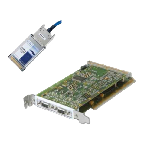
Aim APE429-32 User manual

APE429-32 Hardware Manual
i
Hardware
Manual
V01.00 Rev. A
July 2016
32 Channels
ARINC429 Test & Simulation Module
For PCI Express
APE429-32


APE429-32 Hardware Manual
i
APE429-32
32-Channels
ARINC429 Test & Simulation Module
for PCI Express
V01.00 Rev. A
July 2016
AIM No:
60-121B6-16-0100-A
Hardware
Manual

APE429-32 Hardware Manual
ii
AIM –Gesellschaft für angewandte Informatik und Mikroelektronik mbH
AIM GmbH
Sasbacher Str. 2
D-79111 Freiburg / Germany
Phone +49 (0)761 4 52 29-0
Fax +49 (0)761 4 52 29-33
AIM UK Office
Cressex Enterprise Centre, Lincoln Rd.
High Wycombe, Bucks. HP12 3RB / UK
Phone +44 (0)1494-446844
Fax +44 (0)1494-449324
AIM GmbH –Munich Sales Office
Terofalstr. 23a
D-80689 München / Germany
Phone +49 (0)89 70 92 92-92
Fax +49 (0)89 70 92 92-94
AIM USA LLC
Seven Neshaminy Interplex
Suite 211 Trevose, PA 19053
Phone 267-982-2600
Fax 215-645-1580
© AIM GmbH 2016
Notice: The information that is provided in this document is believed to be accurate.
No responsibility is assumed by AIM GmbH for its use. No license or rights are granted
by implication in connection therewith. Specifications are subject to change without
notice.

APE429-32 Hardware Manual
iii
DOCUMENT HISTORY
The following table defines the history of this document. Appendix A provides a more
comprehensive list of changes made with each version.
Version
Cover Date
Created by
Description
V01.00 Rev. A
12.07.2016
S.Thota
First Released Version

APE429-32 Hardware Manual
iv
THIS PAGE INTENTIONALLY LEFT BLANK

APE429-32 Hardware Manual
v
TABLE OF CONTENTS
Section Title Page
1Introduction.............................................................................................................7
1.1 General....................................................................................................................................... 7
1.2 How This Manual is organized................................................................................................. 8
1.3 Applicable Documents.............................................................................................................. 8
1.3.1 Industry Documents................................................................................................................ 8
1.3.2 Product Specific Documents................................................................................................... 8
2Installation...............................................................................................................9
2.1 Preparation and Precaution for Installation ........................................................................... 9
2.2 Installation Instructions............................................................................................................ 9
2.3 Connecting to other Devices ................................................................................................. 10
2.3.1 APE429-32 Front panel Connector Pinout ........................................................................... 11
2.4 Front Panel LEDs .................................................................................................................... 12
3Structure of the APE429-32 .................................................................................13
3.1 PCI-Express bus and BIU-I/O FPGA...................................................................................... 14
3.1.1 Global RAM Interface and Arbitration................................................................................... 14
3.1.2 Boot up.................................................................................................................................. 14
3.2 Global RAM.............................................................................................................................. 14
3.3 BIU-Processors (BIP).............................................................................................................. 14
3.4 ARINC-429 Encoder ................................................................................................................ 15
3.5 ARINC-429 Decoder ................................................................................................................ 15
3.6 External Trigger Output.......................................................................................................... 15
3.7 IRIG- and Time Code Section................................................................................................. 15
3.7.1 Time Code Encoder/Decoder ............................................................................................... 16
3.7.2 Time Tag Methods................................................................................................................ 16
3.7.3 Board to Board (B2B) connector as IRIG In/Out .................................................................. 17
3.8 Board to Board Connector (B2B connector)........................................................................ 18
3.8.1 General Purpose Discrete Inputs/Outputs (GPIO) ............................................................... 19
3.8.2 IRIG-B................................................................................................................................... 19
4Technical data.......................................................................................................21
5Notes .....................................................................................................................25
5.1 Acronyms................................................................................................................................. 25
6Certificate of Volatility..........................................................................................27

APE429-32 Hardware Manual
vi
LIST OF FIGURES
Figure Title Page
Figure 2-1: Front Panel view..........................................................................................10
Figure 2-2: Status LED view..........................................................................................12
Figure 3-1: Block Diagram of APE429-32......................................................................13
Figure 3-2 : IRIG Jumper...............................................................................................17
Figure 3-3 : 16-pin Ribbon Cable Connector.................................................................18
Figure 3-4 : Ribbon Cable / Cable connection...............................................................19
LIST OF TABLES
Figure Title Page
Table 2-1 : Pin assignment APE429-32.........................................................................11
Table 2-2: Front Panel LED description.........................................................................12
Table 3-1: IRIG-B: Binary Coded Time Tag...................................................................16
Table 3-2 : Pin out B2B connector.................................................................................18

1. Introduction
APE429-32 Hardware Manual
7
1 INTRODUCTION
1.1 General
This document comprises the Hardware User’s Manual for the PCI-Express APE429-
32, which implements 32 transmit and receive ARINC-429 channels, based on the PCI-
Express communication standard. The document covers the hardware installation,
board connections, technical data and a general description of the hardware
architecture. For programming information please refer to the documents listed in the
'Applicable Documents' section.
The APE429-32 is a member of AIM’s new family of advanced PCI-Express module for
analysis, simulation, monitoring and testing of ARINC429 channels providing 32
channels. The PCI-Express Interface is 1-lane wide and working with 2.5 Gbit/s in
transmits and receive direction.
Each channel is software configurable in runtime as a fixed amplitude Transmitter or
Receiver.
On the transmit channels, the APE429-32 acts as an autonomously operating bus traffic
simulator, supporting multiple modes of transmission sequencing. Full error injection
capabilities are available, whereby the error injection is programmable individually for
each channel and label. For special transmission operating modes the parity bit can be
used alternatively as an additional data bit. The rise and fall time of the bus signals are
individually programmable by software for each transmit channel.
For the receive channels, the APE429-32provides an advanced monitor and analyser
function with unique on-board error detection, triggering and filtering capabilities.
Monitor and analyser functions are available concurrently and independent from each
other. The hardware architecture provides resources to guarantee that the performance
of one function is not affected by the current load of the other function. The rise and fall
times of the bus signals are individually programmable for each receive channel. To
adapt to different transmit speeds, the transmission rate can be varied in discrete steps
between approximately 90 and 120Kbits on the high speed bus and between 11.5 and
16.0Kbits on the low speed lines.
The hardware architecture provides ample resources (i.e. processing capability and
memory) to guarantee, that all specified interface functions are available concurrently
and to full performance specifications.
The advanced architecture uses a special processor for the ARINC-429 stream. A
powerful Memory Arbiter is implemented in a Field Programmable Gate Array (FPGA).
This FPGA supports both, the interface to the application and driver software tasks
running on the host computer and assists the communication for data transfer. This
feature expands the capability of the APE429-32 module to that of a high level
instrument. To fulfill the real-time requirements of a typical avionic type data bus
system, a high performance 32bit RISC processor (BIP) is implemented.
1. Introduction
APE429-32 Hardware Manual
8
A free-wheeling IRIG-B Time code Encoder/Decoder is implemented on the APE429-32
to satisfy the requirements of 'multi-channel time tag synchronization' on the system
level. The IRIG-B compatible amplitude modulated sine wave output allows the
synchronization of any external module implementing IRIG-B time stamping.
The module can be installed in standard in PCI-Express slots.
1.2 How This Manual is organized
This APE429-32 Hardware Manual is comprised of the following sections.
Section 1 - INTRODUCTION - Contains an overview of this manual.
Section 2 - INSTALLATION - Describes the steps required to install the APE429-32
device and connect the device to other external 429 interfaces, IRIG-B,
and trigger out.
Section 3 - STRUCTURE OF THE APE429-32 - Describes the physical hardware
interfaces on the APE429-32 using a block diagram and a description of
each main component
Section 4 - TECHNICAL DATA - describes the technical specification of the
APE429-32.
1.3 Applicable Documents
The following documents shall be considered to be a part of this document to the extent
that they are referenced herein. In the event of conflict between the documents
referenced and the contents of this document, the contents of this document shall have
precedence.
1.3.1 Industry Documents
[1] PCI Express BUS Specification; PCI-SIG Revision 1.1
1.3.2 Product Specific Documents
[2] AIM - Reference Manual APE429-32 Application Interface Library: Detailed
description of the programming interface between the Host Carrier board and the
onboard driver software.

2. Installation
APE429-32 Hardware Manual
9
2 INSTALLATION
2.1 Preparation and Precaution for Installation
The APE429-32 features full PCI Plug and Play capability; therefore, there are no
jumpers or switches on the board that require modification by the user in order to
interface to the PCI bus.
It is recommended to use a wrist strap for any installations. If there is no wrist wrap
available, then touch a metal plate on your system to ground yourself and discharge any
static electricity during the installation work.
2.2 Installation Instructions
The following instructions describe how to install the APE429-32 module in your PCIe
slot system. Please follow the instructions carefully, to avoid any damage on the device.
To Install the APE429-32
1. Shutdown your system and all peripheral devices.
2. Unplug the power cord from the wall outlet. (Inserting or removing modules
with power applied may result in damage to module devices).
3. Remove the system cover to gain access to the system slots.
4. Find a free PCIe slot in your system.
5. Remove the slot bracket from the slot you have chosen and put it aside.
6. Align the APE429-32 card slot connector with the PCIe slot and gently lower
the card into the free slot.
7. Secure the card to the PCIe slot with the screw you removed from the metal
plate. Ensure the module is seated properly in the slot connector.
8. Replace the cover of your system.
9. Connect the system to the power source. Turn on the power of your system.

2. Installation
APE429-32 Hardware Manual
10
2.3 Connecting to other Devices
The connection to other devices is done via a SCSI-3 female connector.
The Front panel have 32 ARINC429 channels, IRIG IN/OUT and Trigger OUT.
The APE429-32 implementation has the capability to share the I/O- pins. This means
each ARINC429 channel can be used as Transmit or Receive channel, but only one
operation mode is possible at one time. The pinout is listed below.
Figure 2-1: Front Panel view

2. Installation
APE429-32 Hardware Manual
11
2.3.1 APE429-32 Front panel Connector Pinout
68 pin SCSI-3 female connector, Downward Compatibility Mode
Pin
No.
Signal
Direction
Type
Pin No.
Signal
Direction
Type
1
TxRx_True_1
Bidir.
35
TxRx_Comp_1
Bidir.
2
TxRx_True_2
Bidir.
36
TxRx_Comp_2
Bidir.
3
TxRx_True_3
Bidir.
37
TxRx_Comp_3
Bidir.
4
TxRx_True_4
Bidir.
38
TxRx_Comp_4
Bidir.
5
TxRx_True_5
Bidir.
39
TxRx_Comp_5
Bidir.
6
TxRx_True_6
Bidir.
40
TxRx_Comp_6
Bidir.
7
TxRx_True_7
Bidir.
41
TxRx_Comp_7
Bidir.
8
TxRx_True_8
Bidir.
42
TxRx_Comp_8
Bidir.
9
TxRx_True_9
Bidir.
43
TxRx_Comp_9
Bidir.
10
TxRx_True_10
Bidir.
44
TxRx_Comp_10
Bidir.
11
TxRx_True_11
Bidir.
45
TxRx_Comp_11
Bidir.
12
TxRx_True_12
Bidir.
46
TxRx_Comp_12
Bidir.
13
TxRx_True_13
Bidir.
47
TxRx_Comp_13
Bidir.
14
TxRx_True_14
Bidir.
48
TxRx_Comp_14
Bidir.
15
TxRx_True_15
Bidir.
49
TxRx_Comp_15
Bidir.
16
TxRx_True_16
Bidir.
50
TxRx_Comp_16
Bidir.
17
TxRx_True_30
Bidir.
51
TxRx_Comp_30
Bidir.
18
TxRx_True_31
Bidir.
52
TxRx_Comp_31
Bidir.
19
TxRx_True_17
Bidir.
53
TxRx_Comp_17
Bidir.
20
TxRx_True_18
Bidir.
54
TxRx_Comp_18
Bidir.
21
TxRx_True_19
Bidir.
55
TxRx_Comp_19
Bidir.
22
TxRx_True_20
Bidir.
56
TxRx_Comp_20
Bidir.
23
TxRx_True_21
Bidir.
57
TxRx_Comp_21
Bidir.
24
TxRx_True_22
Bidir.
58
TxRx_Comp_22
Bidir.
25
TxRx_True_23
Bidir.
59
TxRx_Comp_23
Bidir.
26
TxRx_True_24
Bidir.
60
TxRx_Comp_24
Bidir.
27
TxRx_True_29
Bidir.
61
TxRx_Comp_29
Bidir.
28
GND
Pow.
62
TRIGGER_OUT
OUT
29
IRIG_IN
IN
63
IRIG_OUT
OUT
30
TxRx_True_25
Bidir.
64
TxRx_Comp_25
Bidir.
31
TxRx_True_26
Bidir.
65
TxRx_Comp_26
Bidir.
32
TxRx_True_27
Bidir.
66
TxRx_Comp_27
Bidir.
33
TxRx_True_28
Bidir.
67
TxRx_Comp_28
Bidir.
34
TxRx_True_32
Bidir.
68
TxRx_Comp_32
Bidir.
Table 2-1 : Pin assignment APE429-32

2. Installation
APE429-32 Hardware Manual
12
2.4 Front Panel LEDs
Five sub-miniature LEDs, located at the front panel, indicate the module status. The
LEDs are located in a quadruple LED-Array on the physical interface daughterboard.
Figure 2-2: Status LED view
LED Name
Colour
Description
ACTIVITY
Green
LED flashes If data is transmitted on any channel.
FAIL
Red
LED illuminates if an error during the BIU self-test occurs.
RX-ERR
Red
LED flashes if an error on any channel is detected.
RX-ERR-
LATCH
Red
LED illuminates if an error on any channel is detected
(stored error).
Table 2-2: Front Panel LED description

3. Structure of the APE429-32
APE429-32 Hardware Manual
13
3 STRUCTURE OF THE APE429-32
The structure of the APE429-32 is shown in Figure 3-1. This card comprises the
following main sections:
PCI Express bus and BIU-IO FPGA
Global RAM
BIU Processors Section (2-BIU’s)
Physical I/O Interface with 32 ARINC-429 channels and Trigger out
IRIG- Time Code Proc. with free-wheeling function and Sine Wave Output
Boot-Up Flash
Figure 3-1: Block Diagram of APE429-32

3. Structure of the APE429-32
APE429-32 Hardware Manual
14
3.1 PCI-Express bus and BIU-I/O FPGA
The new common FPGA architecture of AIM’s PCI-Express family includes a complete
PCI-Express bus logic (which is translated to a legacy PCI interface using an external
bridge component) and the 2-BIU processors logic. This programmable device
implements the following features:
PCI Express 1.1 compliant bus interface
Global RAM interface and arbitration
Boot function
SPI controller for update programming
ARINC-429 Encoder
ARINC-429 Decoder
IRIG Encoder and decoder support
External Trigger Output
3.1.1 Global RAM Interface and Arbitration
The common FPGA implements a Global RAM arbiter, which controls the Global RAM
access between both participants, the Host through the PCI-Express bus and the BIU
processor.
3.1.2 Boot up
To provide maximum flexibility and upgradeability, the FPGA device and the processors
are booted automatically from dedicated SPI-Flashes after power up.
3.2 Global RAM
The Global RAM is shared between both BIU processors (BIP) and the Host-Card Bus.
The arbitration is handled by the common FPGA. It has access to the common Global
RAM via a 32 bit wide data port.
3.3 BIU-Processors (BIP)
There are two physical BIU processors. Each BIP consists of an ultra-low power, high
performance 32bit RISC processor.

3. Structure of the APE429-32
APE429-32 Hardware Manual
15
3.4 ARINC-429 Encoder
The encoder converts the parallel data into a serial ARINC429 encoded data stream
and appends the parity and the gap bits. The programmable frame-time between two
labels can be set in the range from 0 up to 255 ARINC429 bits.
The encoder provides the following error injection capabilities:
Gap Error (-1 bit)
Bit count Error (+/- 1 bit)
Coding Error (fixed at bit position 12)
Parity Error (if no special transmission mode is chosen)
3.5 ARINC-429 Decoder
The decoder converts the serial received data stream into a parallel data double word
and generates an additional 16 bit report for each received label. The decoder
measures the gap time between two labels for gap error detection and bus load traffic
detection.
The decoder provides the following error detection capabilities:
Gap Error Detection
Bit count Error Detection
Coding Error Detection
Parity Error Detection (if no special transmission mode is chosen)
3.6 External Trigger Output
One Trigger output is provided on APE429-32 variant.
The Trigger output is TTL level compatible. Filter circuitry is provided at the trigger
output to cover Electromagnetic Compatibility (EMC) aspects.
3.7 IRIG- and Time Code Section
The main functions of the Time Code Processor (TCP) are:
IRIG-B compatible Time Code Decoder function
Time code Encoder –IRIG-B compatible Time Encoder function

3. Structure of the APE429-32
APE429-32 Hardware Manual
16
3.7.1 Time Code Encoder/Decoder
The generated time code signal is an IRIG-B compatible sinusoidal waveform. The time
code information can be used for time-tagging and multi-channel synchronization. On
the APE429-32 a new generation IRIG-B section is implemented with a free-wheeling
IRIG functionality. If no external IRIG signal is detected, the TCP switches automatically
to the free-wheeling mode. Also, if an external IRIG-B signal is detected in free-
wheeling mode, the Time tag is automatically synchronized to this external IRIG-B
signal.
The time tag on the board is generated in the format explained in the following table:
Time Element
Number of bits
DAYS of Year
9
HOURS of Day
5
MINUTES of Hour
6
SECONDS of Minute
6
MICROSECONDS of Second
20
Summary
46 (6 Bytes, stored in two 32bit words)
Table 3-1: IRIG-B: Binary Coded Time Tag
3.7.2 Time Tag Methods
Besides the ARINC429 receive and transmit signals, the 68 pin SCSI-3 connector
comprises one Trigger output signal as well as the IRIG-B- input and output as listed at
all previous described Connector Pinout tables.
The IRIG-IN and IRIG-OUT signals shall be connected depending on the Time
synchronisation method used as shown below.
1. Single AIM-Module No External IRIG-B Source
No connection required
2. Multiple AIM-Modules with No Common Synchronization Requirement
No connection required
3. Single or Multiple AIM-Module(s) with External IRIG-B Source
Connect external IRIG-B source to IRIG-IN and GND of all modules
4. Multiple AIM-Modules with No External IRIG-B Source Internally
Synchronized.
Connect the IRIG-OUT signal and the GND of the module you have chosen as
the time master to all IRIG-IN signals (including the time master).

3. Structure of the APE429-32
APE429-32 Hardware Manual
17
3.7.3 Board to Board (B2B) connector as IRIG In/Out
Normally for connecting the IRIG Input and/or Output the 68 pin SCSI-3 female
connector is used for wiring. Follow the instructions below if the B2B connector is used
instead.
The IRIG-B output signal can be manually switched to the B2B connector by setting the
jumper position to “Master-Mode”.
To avoid signal collision only one board should drive the IRIG output signal.
The figure 3.-2 below shows the on-board Board IRIG Master/Slave jumper (J0504) on
the APE429-32:
Figure 3-2 : IRIG Jumper
If the board receives the IRIG signal, it is in IRIG Slave-Mode, if the board transmits the
IRIG signal, it is in IRIG Master-Mode.
To set a board to IRIG Master-Mode (IRIG output), the jumper has to be set to position
1 and position 2.
To set a board to IRIG Slave-Mode (IRIG Input), the jumper has to be set to position 2
and position 3 or it can be removed (no jumper installed).
The on board generated IRIG output signal is available simultaneously on the B2B
connector (if set to IRIG Master-Mode) and on the 429 Physical Bus Interface board
(429 PBI).
To receive an external IRIG signal either the PBI IRIG input or the B2B connector IRIG
input (IRIG Slave Mode) can be used (exclusive).
Pos1
Pos3

3. Structure of the APE429-32
APE429-32 Hardware Manual
18
3.8 Board to Board Connector (B2B connector)
The Board to Board connector provides an additional one pin combined IRIG-B Master-
Output/Slave Input on a 16-pin ribbon cable connector (mounted on the upper right
corner, see figure 3.13-1).
Figure 3-3 : 16-pin Ribbon Cable Connector
The connector provides the following signals:
Pin
Signal Name
Comments
1
Reserved
No Connection
2
Reserved
No Connection
3
Reserved
No Connection
4
Reserved
No Connection
5
Reserved
No Connection
6
Reserved
No Connection
7
Reserved
No Connection
8
Reserved
No Connection
9
Reserved
No Connection
10
Reserved
No Connection
11
Reserved
No Connection
12
IRIG
Master-Output / Slave-Input (select via
J1702)
13
GND
14
Reserved
No Connection
15
Reserved
No Connection
16
Reserved
No Connection
Table 3-2 : Pin out B2B connector
For a detailed description how to select between IRIG Master and Slave operation
please refer to chapter 3.7.3 (IRIG Master/Slave Jumper)
For connecting multiple APE429 boards together a 16-pin standard ribbon cable with
coded ribbon cable connector is used. It’s important to use coded connectors to avoid
damages caused by signal collisions.
Pin 16
Pin 2
Pin 1
Table of contents
Other Aim Control Unit manuals