Aiwa XR-MS3 User manual

SERVICE MANUAL
DATA
COMPACT DISC
STEREO SYSTEM
BASIC TAPE MECHANISM : 2ZM-1 R10NM/
2ZM-1 YR10NC
BASIC CD MECHANISM : TN-CCD1001-902M
XR-MS3
U, HC
S/M Code No. 09-00A-422-6S4
SUPPLEMENT
•This Service Manual contains the additional information “CD ELECTRICAL SECTION”
for the model XR-MS3 (U,HC). If requiring the other information, see Service Manual of
XR-MS3 (U,EZ), (S/M Code No. 09-002-422-6R1),
XR-MS3 (HC), (S/M Code No. 09-008-422-6R2).

– 2 –
CLASS 1 LASER PRODUCT
KLASSE 1 LASER PRODUKT
LUOKAN 1 LASER LAITE
KLASS 1 LASER APPARAT
This set employs laser. Therefore, be sure to follow carefully
the instructions below when servicing.
WARNING!!
WHEN SERVICING, DO NOT APPROACH THE LASER
EXIT WITH THE EYE TOO CLOSELY. IN CASE IT IS
NECESSARY TO CONFIRM LASER BEAM EMISSION.
BE SURE TO OBSERVE FROM A DISTANCE OF MORE
THAN 30cm FROM THE SURFACE OF THE OBJEC-
TIVE LENS ON THE OPTICAL PICK-UP BLOCK.
sCaution: Invisible laser radiation when
open and interlocks defeated avoid
exposure to beam.
sAdvarsel: Usynlig laserståling ved åbning,
når sikkerhedsafbrydere er ude af funktion.
Undgå udsættelse for stråling.
VAROITUS!
Laiteen Käyttäminen muulla kuin tässä käyttöohjeessa
mainitulla tavalla saataa altistaa käyt-täjän
turvallisuusluokan 1 ylittävälle näkymättömälle
lasersäteilylle.
VARNING!
Om apparaten används på annat sätt än vad som
specificeras i denna bruksanvising, kan användaren
utsättas för osynling laserstrålning, som överskrider
gränsen för laserklass 1.
PROTECTION OF EYES FROM LASER BEAM DURING SERVICING
CAUTION
Use of controls or adjustments or performance of proce-
dures other than those specified herin may result in
hazardous radiation exposure.
ATTENTION
L’utillisation de commandes, réglages ou procédures
autres que ceux spécifiés peut entraîner une dangereuse
exposition aux radiations.
ADVARSEL
Usynliglaserstålingvedåbning,nårsikkerhedsafbrydereer
ude af funktion. Undgå udsættelse for stråling.
This Compact Disc player is classified as a CLASS 1
LASER product.
The CLASS 1 LASER PRODUCT label is located on the
rear exterior.
PICK-UP ASSY
VED0375-TN
Precaution to replace Optical block
(VED0375-TN)
Body or clothes electrostatic potential could
ruin laser diode in the optical block. Be sure
ground body and workbench, and use care the
clothes do not touch the diode.
1) After the connection, remove solder shown in
right figure.
SOLDER

– 3 –
ELECTRICAL MAIN PARTS LIST
DESCRIPTIONREF. NO. KANRI
NO.
PART NO. KANRI
NO.
REF. NO. DESCRIPTIONPART NO.
IC
8A-CG5-602-010 IC,CXP84332-169Q
87-A21-533-030 IC,CXD2587Q
87-A21-596-040 IC,CXA2570N
87-A20-711-040 IC,BA5970FP
87-A21-777-040 IC,BA6289F
87-A21-847-040 IC,UPC842G2
TRANSISTOR
87-A30-541-040 C-TR,2SB736
87-A30-542-040 C-TR,2SD999(CL)
87-A30-543-040 C-TR,FP1F3P
89-316-236-080 C-TR,2SC1623(L6)
DIODE
87-020-331-080 DIODE,DAN202K
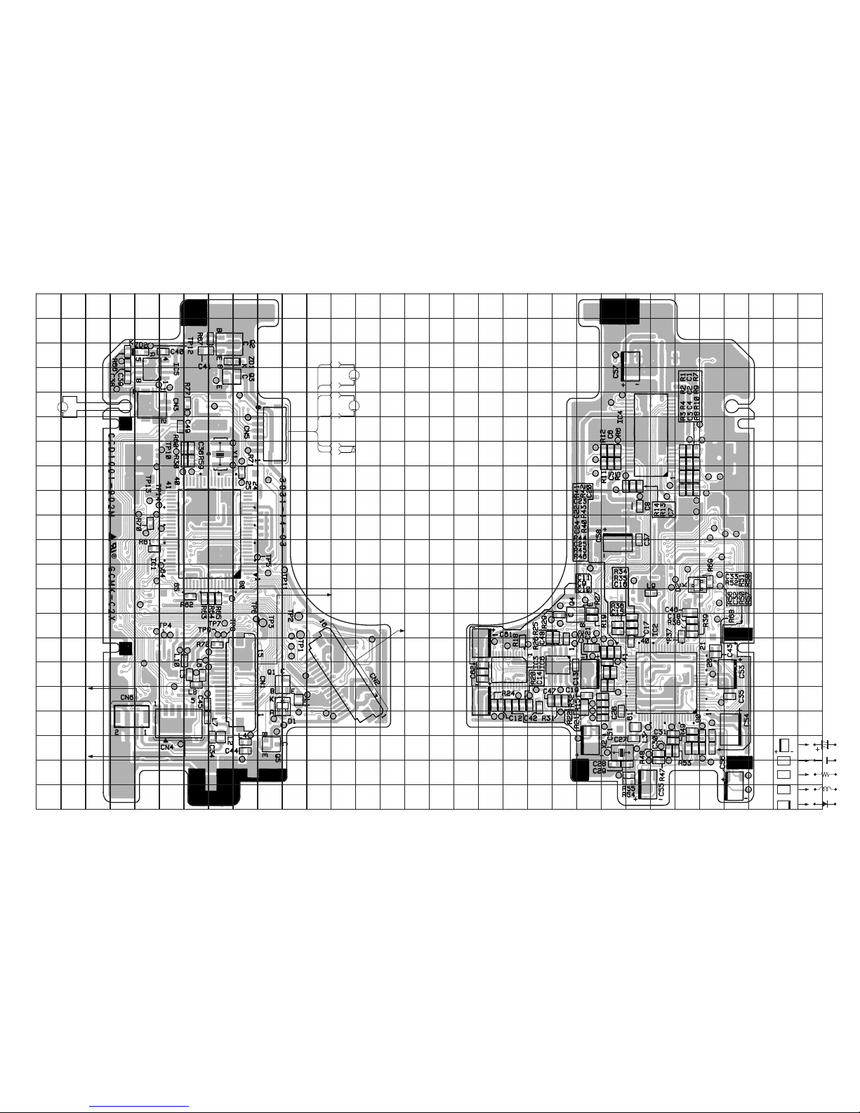
MAIN C.B
C2 87-012-272-080 C-CAP,680P-50V
C4 87-012-272-080 C-CAP,680P-50V
C5 87-010-787-080 C-CAP,0.022U-25V
C6 87-010-787-080 C-CAP,0.022U-25V
C8 87-010-831-080 C-CAP,0.1U-16V
C9 87-010-831-080 C-CAP,0.1U-16V
C10 87-010-831-080 C-CAP,0.1U-16V
C11 87-010-831-080 C-CAP,0.1U-16V
C12 87-012-191-080 C-CAP,68P-50V
C13 87-010-831-080 C-CAP,0.1U-16V
C14 87-012-170-080 C-CAP,8P-25V
C15 87-012-199-080 C-CAP,220P-50V
C16 87-010-831-080 C-CAP,0.1U-16V
C17 87-012-199-080 C-CAP,220P-50V
C19 87-010-831-080 C-CAP,0.1U-16V
C21 87-012-358-080 C-CAP,0.47U-16V
C22 87-012-199-080 C-CAP,220P-50V
C24 87-012-276-080 C-CAP,1500P-50V
C25 87-010-829-080 C-CAP,0.047U-25V
C26 87-010-831-080 C-CAP,0.1U-16V
C27 87-010-831-080 C-CAP,0.1U-16V
C28 87-012-182-080 C-CAP,27P-50V
C29 87-012-182-080 C-CAP,27P-50V
C30 87-012-272-080 C-CAP,680P-50V
C31 87-012-197-080 C-CAP,150P-50V
C32 87-012-272-080 C-CAP,680P-50V
C33 87-012-197-080 C-CAP,150P-50V
C34 87-010-831-080 C-CAP,0.1U-16V
C35 87-010-831-080 C-CAP,0.1U-16V
C36 87-010-831-080 C-CAP,0.1U-16V
C37 87-010-831-080 C-CAP,0.1U-16V
C38 87-010-831-080 C-CAP,0.1U-16V
C39 87-010-831-080 C-CAP,0.1U-16V
C40 87-010-831-080 C-CAP,0.1U-16V
C41 87-012-358-080 C-CAP,0.47U-16V
C42 87-010-831-080 C-CAP,0.1U-16V
C43 87-010-831-080 C-CAP,0.1U-16V
C44 87-012-188-080 C-CAP,47P-50V
C46 87-012-358-080 C-CAP,0.47U-16V
C47 87-012-188-080 C-CAP,47P-50V
C48 87-012-188-080 C-CAP,47P-50V
C49 87-010-831-080 C-CAP,0.1U-16V
C51 87-A11-030-080 C-CAP,E 10U-25V
C52 87-A11-156-080 C-CAP,E 22U-25V
C53 87-A11-156-080 C-CAP,E 22U-25V
C54 87-A11-028-080 C-CAP,E 100U-10V
C55 87-A11-030-080 C-CAP,E 10U-25V
C56 87-A11-030-080 C-CAP,E 10U-25V
C57 87-A11-156-080 C-CAP,E 22U-25V
C58 87-A11-156-080 C-CAP,E 22U-25V
C61 87-A11-156-080 C-CAP,E 22U-25V
C62 87-A11-156-080 C-CAP,E 22U-25V
CN1 87-A61-488-080 CONN,15P
CN2 87-009-214-080 CONN,16P
CN3 87-099-440-080 CONN,2P
CN4 87-A61-477-080 CONN,5P
CN5 87-A61-478-080 CONN,6P
L1 87-005-906-080 C-COIL,10UH
L2 87-A50-665-080 C-COIL,100UH
L3 87-A50-665-080 C-COIL,100UH
L4 87-A50-623-080 C-COIL,BLM11A102S
L5 87-A50-623-080 C-COIL,BLM11A102S
L6 87-A50-623-080 C-COIL,BLM11A102S
L7 87-A50-623-080 C-COIL,BLM11A102S
L8 87-A50-623-080 C-COIL,BLM11A102S
L9 87-A50-623-080 C-COIL,BLM11A102S
L10 87-A50-623-080 C-COIL,BLM11A102S
SW5 S6-418-040-040 DET SW ESE11HS2
X1 87-A70-251-080 VIB,CSTCC10.0MG 10MHZ
X2 87-A70-295-080 VIB,CSACV16.93MXJ040
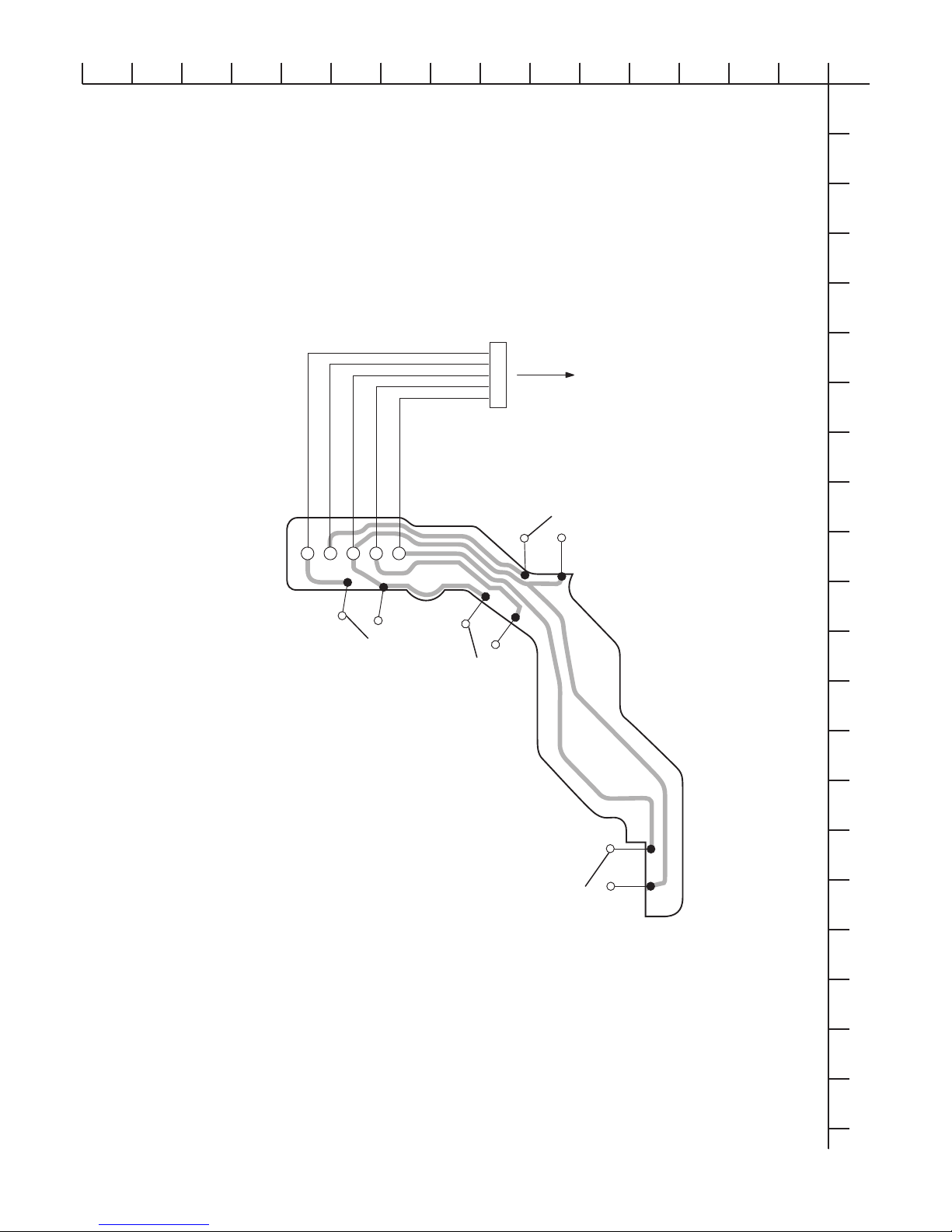
SW C.B
SW1 S6-418-040-030 DET SW ESE22 MH3
SW2 S6-418-040-020 DET SW ESE22 MH1
SW3 S6-418-040-020 DET SW ESE22 MH1
SW4 S6-418-040-030 DET SW ESE22 MH3
TRANSISTOR ILLUSTRATION
B
C
E
2SB736
2SD999(CL)
FP1F3P
2SC1623(L6)

WIRING – 1 (MAIN)
NOTE
Cxxx
Rxxx
Lxxx
ZDxxx
14
15
28
12
45
8
13
24
TO MAIN UNIT
TO MAIN UNIT
TO PICK-UPASSSY
VED0375-TN
TO SW C.B
M
M
M
M3
(LOADING MOTOR)
M1
(SLED MOTOR)
M2
(SPINDLE MOTOR)
SW5
(PICK UP DET SW)
6
5
4
3
2
1
– 4 –
MAIN C.B (COMPONENT SIDE) MAIN C.B (CONDUCTOR SIDE)
876543211345678
A
B
C
D
E
F
G
H
I
J
K
L
M
N
O
P
Q
R
S
T
U
2
A
B
C
D
E
F
G
H
I
J
K
L
M
N
O
P
Q
R
S
T
U
9 10 11 12 13 14 15 16910111213141516

WIRING – 2 (SW)
– 5 –
123456789101112131415
A
B
C
D
E
F
G
H
I
J
K
L
M
N
O
P
Q
R
S
T
U
TO MAIN C.B
CN4
SW3
SW4
SW1
SW2
(DISC DET)
(DISC DET)
(DISC DET)
(DISC DET)
SW C.B

MAIN C.B
SW C.B
TO MAIN UNITTO MAIN UNIT
SIGNAL
: PB (ANALOG)
*** : No Mount
: PB (DIGITAL)
Digital
Output
PICK-UP
VED0375-TN
M
M
M
M3
LOADING
MOTOR
M1
SLED
MOTOR
M2
SPINDLE
MOTOR
SW5
PICK UP DET SW
ESE11HS2
LD SW
AMP
RF AMP
RF AMP
SYSTEM CONTROL
RESET
REG
SW
AMP
LD SW
MOTOR
DRIVER
LOADING
MOTOR
DRIVER
DIGITAL SERVO,
DAC,DSP
DIGITAL FILTER
B2B-PH
-SM3-TB
1
2
3
4
5
SW4
(DISC DET)
SW3
(DISC DET)
SW1
(DISC DET)
SW2
(DISC DET)
Communication Lines
– 6 –
SCHEMATIC DIAGRAM

– 7 –
IC BLOCK DIAGRAM

– 8 –
1 SQSO O Sub-Q 80-bit, PCM peak and level data output. CD TEXT data output.
2 SQCK I SQSO Clock input for reading.
3 XRST I System reset. Reset at "L".
4 SYSM I Muting input. Muted at "H".
5 DATA I Serial data input from CPU.
6 XLAT I Latch input from CPU. Latches serial data at the trailing edge.
7 CLOK I Clock input for serial data transfer from CPU.
8 SENS O SENS output to CPU.
9 SCLK I Clock input for reading SENS serial data.
10 VDD – Power supply of digital circuits.
11 ATSK I/O Input/output for anti-shock. (Connected to ground)
12 SPOA I Microprocessor extended interface (input A). (Connected to ground)
13 SPOB I Microprocessor extended interface (input B). (Connected to ground)
14 XLON O Microprocessor extended interface (output). (Not used)
15 WFCK O WFCK output. (Not used)
16 XUGF O XUGF output. MNT1 or RFCK is output when switched by command. (Not used)
17 XPCK O XPCK output. MNT0 is output when switched by command. (Not used)
18 GFS O GFS output. MNT3 or XROF is output when switched by command.
19 C2PO O C2PO output. GTOP is output when switched by command.
20 SCOR O Outputs "H" when either Sub-code sync S0 or S1 is detected.
21 COUT I/O Track number count signal input/output. (Not used)
22 MIRR I/O Mirror signal input/output. (Not used)
23 DFCT I/O Defect signal input/output. (Not used)
24 FOK I/O Focus OK signal input/output.
25 LOCK I/O Outputs "H" when GFS sampled by 460 Hz is "H"; "L" when GFS is "L" continuously for 8
samplings. Or, a signal is input when LKIN is "1".
26 MDP O Spindle motor servo control output.
27 SSTP I Disc innermost track detection signal input.
28 SFDR O Sled drive output.
29 SRDR O Sled drive output.
30 TFDR O Tracking drive output.
31 TRDR O Tracking drive output.
32 FFDR O Focus drive output.
33 FRDR O Focus drive output.
34 VSS – Ground of digital circuits.
35 TEST I TEST pin. (Connected to ground)
36 TES1 I TEST pin. (Connected to ground)
37 XTSL I Crystal select input. "L" when 16.9344MHz crystal is used;
"H" when 33.8688MHz crystal is used. (Connected to ground)
38 VC I Center voltage input.
39 FE I Focus error signal input.
Pin No. Pin Name I/O Description
IC, CXD2587Q
IC DESCRIPTION

– 9 –
40 SE I Sled error signal input.
41 TE I Tracking error signal input.
42 CE I Center servo analog input.
43 RFDC I RF signal input.
44 ADIO O For test. (Not used)
45 AVSS0 – Ground of analog circuits.
46 IGEN I Constant current input for OP amp.
47 AVDD0 – Power supply of analog circuits.
48 ASYO O EFM full-swing output ("L" = VSS, "H" = VDD).
49 ASYI I Asymmetry comparator voltage input.
50 BIAS I Asymmetry circuit constant current input.
51 RFAC I EFM signal input.
52 AVSS3 – Ground of analog circuits.
53 CLTV I VCO1 control voltage input for multiplication.
54 FILO O Filter output for master PLL (Slave: Digital PLL).
55 FILI I Filter input for master PLL.
56 PCO O Charge pump output for master PLL.
57 AVDD3 – Power supply of analog circuits.
58 VSS – Ground of digital circuits.
59 VDD – Power supply of digital circuits.
60 DOUT O Digital Out output.
61 LRCK O D/A interface LR clock output f=Fs. (Not used)
62 PCMD O D/A interface serial data output (2's COMP, MSB first). (Not used)
63 BCK O D/A interface bit clock output. (Not used)
64 EMPH O Outputs "H" when disc to be played is applied with emphasis; "L" when disc is not applied with
emphasis. (Not used)
65 XVDD – Power supply of master clock.
66 XTAI I Crystal oscillator input. External master clock is input to this pin.
67 XTAO O Crystal oscillator output.
68 XVSS – Ground of master clock.
69 AVDD1 – Power supply of analog circuits.
70 AOUT1 O Lch analog output.
71 AIN1 I Lch OP amp input.
72 LOUT1 O Lch LINE output.
73 ~ 74 AVSS1, AVSS2 – Ground of analog circuits.
75 LOUT2 O Rch LINE output.
76 AIN2 I Rch OP amp input.
77 AOUT2 O Rch analog output.
78 AVDD2 – Power supply of analog circuits.
79 RMUT O Rch "0" detection flag. (Not used)
80 LMUT O Lch "0" detection flag. (Not used)
Pin No. Pin Name I/O Description

– 10 –
• PCMD is a MSB first, two's complement output.
• GTOP is used to monitor the frame sync protection status. (High: sync protection window released.)
• XUGF is the frame sync obtained from the EFM signal, and is negative pulse. It is the signal before sync
protection.
• XPCK is the inverse of the EFM PLL clock. The PLL is designed so that the falling edge and the EFM
signal transition point coincide.
• The GFS signal goes high when the frame sync and the insertion timing match.
• RFCK is derived from the crystal accuracy, and has a cycle of 136µs.
• C2PO reqresents the data error status.
• XROF is generated when the 16K RAM exceeds the ±4F jitter margin.
Monitor Pin Output Combinations
Command bit
0 0 XUGF XPCK GFS C2PO
0 1 MNT1 MNT0 MNT3 C2PO
10RFCK XPCK XROF GTOP
NOTES
MTSL1 MTSL0 Output Data

– 11 –
CD MECHANISM EXPLODED VIEW 1 / 1
66
44
45
46
67
49
47
50
H
HH
A
A
F
B
B
B
50
AA
A
A
AA
AA
A
B
H
DD
I
H
H
G
E
I
C
41
40
38
37
39
DET SW
ESE22MH1 30
31 32 36
29
28
DET SW ESE22MH3
FD GR(C)
DET SW
ESE11HS2
31
33
34
35
13 14 15
44
48
51
52
53
54
55
58 57
56
60
61
62
65
43
68
59
59
44
24
23
22
25
422
21
68
20
10
11 12
64
63
8
9
8
7
6
2
3
1
PWB
PWB
518
16
17 42 19
26
27

– 12 –
CD MECHANISM PARTS LIST 1 / 1
DESCRIPTIONREF. NO. KANRI
NO.
PART NO. DESCRIPTIONREF. NO. KANRI
NO.
PART NO.
1 S3-031-110-030 EARTH SPR
2 S3-031-110-180 L.P SPRING(L)
3 S3-031-110-010 FRONT BRKT
4 S3-031-113-010 LDG MOTOR ASSY
5 S3-031-110-190 L.P SPRING(R)
6 S3-031-110-050 SUPPORT PL
7 S3-031-110-080 GR MT BLK
8 S9-W03-302-760 NW BLUE 2.9-5-0.3
9 S3-031-110-360 LDG ROLLER(P)
10 S3-031-110-100 LDG GR(3)
11 S3-031-110-090 LDG GR(2)
12 S3-031-110-290 LDG BELT
13 S3-031-113-020 LDG RLR SFT ASSY
14 S9-W07-250-300 LUMIL AR W 2.3-9.8-0.25
15 S3-031-110-120 LDG GR(5)
16 S3-031-050-300 NUT PUSH SPR PL(M)
17 S3-031-050-290 PU M NUI(M)
18 S6-904-160-010 PICK-UP VED0375-TN
19 S3-031-053-040 FEED SCREW(M)ASSY
20 S3-031-050-320 PU SHAFT(M)
21 S3-031-050-330 THRUST SPR(M)
22 S3-031-050-210 LOCK PIN
23 S3-031-050-220 LOCK PIN BL
24 S3-031-050-760 F.M. BASE(A)
25 S3-031-053-010 FEED MOTOR ASSY
26 S3-031-050-280 FD GR BLK(M)
27 S3-030-050-100 PU GEAR(B)
28 S3-031-010-570 UPPER PL(A)
29 S3-031-110-240 SW ACTR
30 S3-031-010-090 SEL ARM (L)
31 S3-031-010-110 S ARM SPRING
32 S3-031-010-080 SEL STOP PL
33 S3-031-010-100 SEL ARM (R)
34 S3-031-010-250 S.L ARM SPRING
35 S3-031-010-240 S.L ARM
36 S3-031-010-580 FIX ARM(R)A
37 S3-031-010-380 LDG GR(6)B
38 S3-031-010-220 LDG GR(6)SPRING
39 S3-031-010-370 FIX PL(R)B
40 S3-031-010-340 FIX ARM(L)B
41 S3-031-010-500 FIX PL(L)Z
42 S3-031-050-310 FD SCREW(M)
43 S3-031-010-530 HUNG DOWN SPRING(A)
44 S3-031-050-240 DAMPER(J)
45 S3-031-010-020 REAR D BRKT
46 S3-031-010-150 TRIG PL SPRING
47 S3-031-010-160 TRIG ARM
48 S3-031-010-120 TRIG LVR
49 S3-031-010-140 TRIG PL
50 S3-031-010-030 DAMPER PIN
51 S3-031-050-360 STOPPER SPR
52 S3-031-050-190 8CM STOPPER SPR PL
53 S3-031-050-230 CLAMPER PLATE
54 S3-031-050-150 CLAMPER
55 S3-031-050-740 CLP ARM(A)
56 S3-031-050-410 8CM STOPPER(M)
57 S3-031-050-140 CLP ARM SPRING
58 S3-031-050-250 CLP ARM SPR(L)
59 S3-031-050-700 D.S ARM COLLAR
60 S3-031-050-720 SP COLLAR
61 S3-031-050-710 D.S ARM SPR
62 S3-031-055-010 DISC SUPPORT ARM ASSY
63 S9-W02-500-900 PW CUT 2.1-4-0.5
64 S3-031-053-050 SPINDLE MOTOR(M)ASSY
65 S3-031-050-730 T.T.BASE(A)
66 S3-031-010-010 FRAME
67 S3-031-010-620 BARNCE SPRING(LR)
68 S3-031-010-610 BARNCE SPRING(R)
A 87-841-034-410 CAMERA B TAPPING SCREW M2-4
B 87-741-033-410 CAMERA SCREW TS.G M2-4
C S9-C04-205-030 CAMERA S TAPPING SCREW M2-5
D 87-267-525-310 CAMERA SCREW M1.7-2.2
E 87-263-036-010 CAMERA TAPPING SCREW B 3 M2-8
F S9-C42-202-010 CAMERA TAPPING SCREW S 3 M2-2
G S9-C45-175-030 CAMERA TAPPING SCREW P3 M1.7-5
H 87-351-549-310 CAMERA B TAPPING SCREW M2-4
I S9-P02-200-310 TAMS SCREW M2-3

2–11, IKENOHATA 1–CHOME, TAITO-KU, TOKYO 110, JAPAN TEL:03 (3827) 3111
Printed in Singapore9301978 0251431
Other manuals for XR-MS3
4
Table of contents
Other Aiwa Stereo System manuals