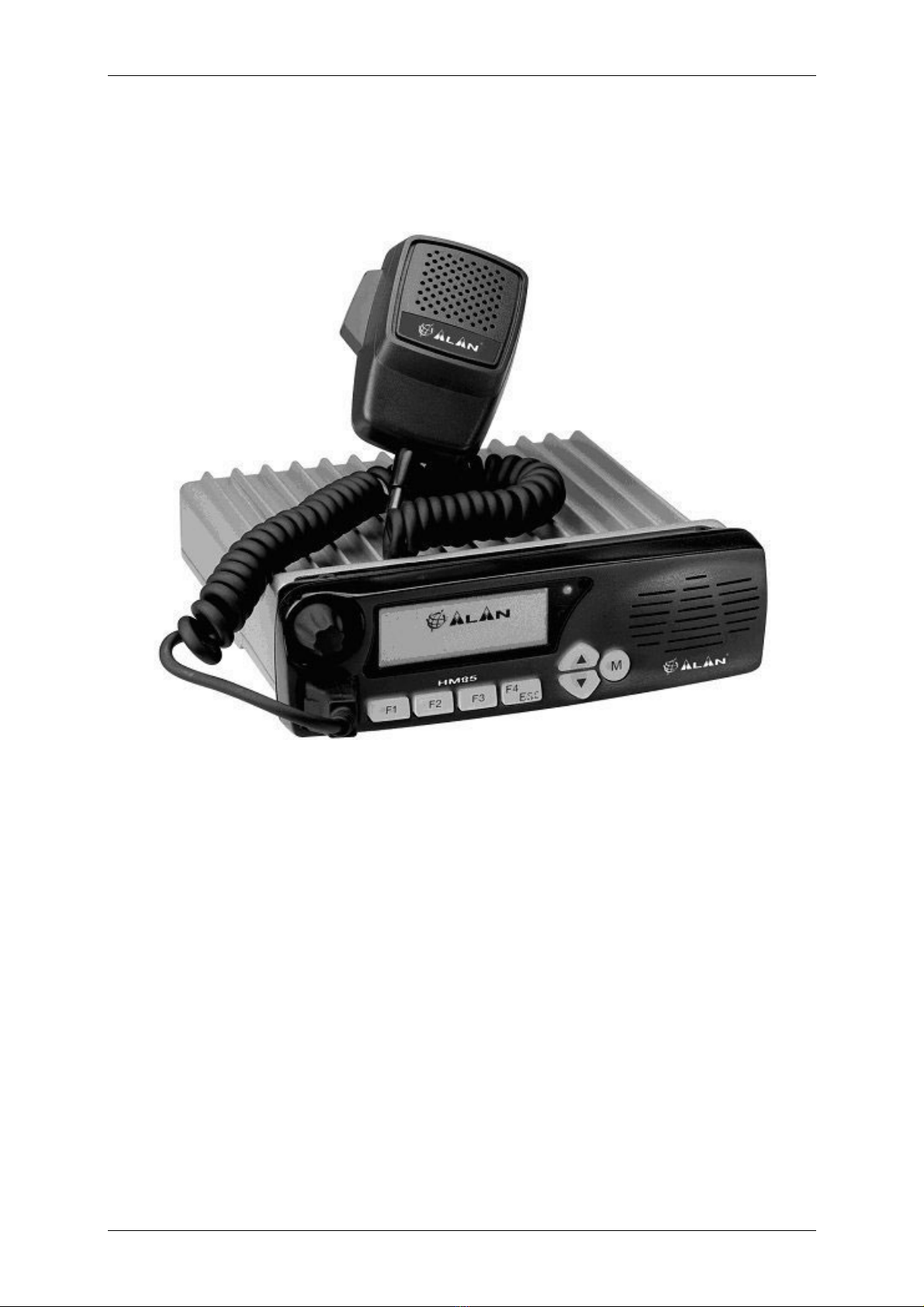
HM135 Service Manual
Preliminary version Page 5 of 13
2.3 Front panel (head) circuitry
The microprocessor DD800 runs off a 8 MHz oscillator which is composed of X800, and R829. DD800 is basically
used to control the LCD unit XT80, to decode the commands coming from the front keypad S801 to S808) as well
as to switch the front LEDs DA800. It is also used to light up the LCD backlight (VD800 to VD805) as well as for
the PTT circuit as over stated.
The negative voltage necessary for the LCD is created by a charge pump which consists of VT815, VT813,
VT812, VD809 and VD808. The output (line –8V) is fed to the regulator DA804:A which outputs the line VD in
order to supply the LCD unit.
The hang-up functions work this way: the line AUX_HOOK is connected to the microphone’s hook and it’s
normally grounded (microphone hooked). When the mike is removed from its hook, the line AUX_HOOK changes
its state driving the transistor VT809. This changes the status of the pin 21 of the microprocessor DD800 which
opens the monitor through a command sent to the main microprocessor DD5 through a serial command.
2.4 VCO / Synthesizer (PLL)
This section basically consists of the Temperature-Compensated Crystal Oscillator (TCXO), Voltage Controlled
Oscillators (VCOs), Synthesizer and the Loop Filter.
2.4.a Temperature-Compensated Crystal Oscillator (TCXO)
The reference oscillator is composed by the temperature compensated crystal X2 and related circuitry (DA1:A.
VD19, VD20, VT21 and VT20), RP2 is used to adjust the oscillator on frequency (12.8 MHz) at room temperature.
The reference oscillator is held within the specifications ±5 ppm from -25 to +55℃.
2.4.b Voltage-Controlled Oscillators
The receive VCO consists of VT11, CV1, VD6 and VD9. This VCO oscillates at 45.1 MHz above the programmed
receive frequency (i.e. from 181.1 to 219.1 MHz for the 135-174 MHz range). The VCO’s oscillating frequency is
tuned by the varactors VD6 and VD9.
The transmitter VCO consists of VT17, CV2, VD11-VD12 and VD13-VD14 and oscillates directly to the TX carrier
frequency range (i.e. from 135 to 174 MHz range). The TX VCO is directly frequency-modulated by means of the
varactor VD15 which is driven by the modulating signal (line A) regulated by the trimmer RP4. This is part of the
double-point modulation and works mainly in high AF modulating frequencies), the other part of the double point-
modulation is explained in the par. “Transmitter Audio Circuits”.
The tuning voltage for the VCOs is supplied from the output of the Loop Filter made with R73, R74, R78, C99,
C100 and C101.
Only one of the VCOs runs at a time. In RX the line RXC (which is obtained from the +8V_RX line coming from
the voltage switch VT41) is high enabling the RX VCO via the transistor VT16. During this time the line TXC
(which is obtained from the +8VTX line coming from the voltage switch VT42) is low, so the TX VCO is disabled.
When the PTT is pressed, the RXC line becomes low switching the RX VCO off. At the same time the line TXC
goes high activating the TX VCO via the transistor VT18.
The output of the VCOs are AC coupled (C91 and C109) and sent to the synthesizer buffer VT19, then sent to
DA5 for an additional buffering. The output of DA5 is connected to the low-pass filter (L27, L28, L29 and related
capacitors), then directly sent to the TX stages (line HET_TX which is sent to the pre-driver amplifier VT24) or RX
stages (line HET_RX which is sent to the RX mixer A1) due to the RF switching action provided by VD16 and
VD17 which are controlled by the lines +8VRX and 8V_TX_F respectively (this last line is obtained from the line
+8VTX passed through the filter created with L52, L53 and related capacitors). The output from the VCO
necessary to feedback the PLL IC DA3 (i.e. line PLL_RF send to pin 8) is directly output from VT19 and fed
through R106, C362 and C134. , whilst the other part of the signal is fed to DA5, then passed through the low-
pass filter (L27, L28, L29, C130, C132, C133 and C131). Diodes VD16 and VD17 act as signal switches in order
to feed the signal to RX or TX stages at the appropriate time according to the switching voltages which are,
respectively, the lines +8VRX and 8V_TX_F.
The PLL IC DA3 receives the reference signal from the TCXO (pin 1) and the feedback from the VCO (pin 8). The
synthesizer is tuned in 5.00 KHz or 6.25 KHz steps. The output from the PLL IC (pin 15 and 16) is used to drive
the PLL charge pump which consists of VT12, VT13, VT14 and VT15, then the charge pumps sent the output to
the PLL filter in order to close the loop.